
[AKD7719-A]
<KM107300> 2011/06
- 1 -
GENERAL DESCRIPTION
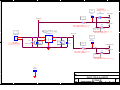
The AKD7719-A is an evaluation kit for the AK7719; a digital signal processor (DSP) with 4 channels
digital data interface. It realizes an easy evaluation of the audio system by just connecting to the target
product via digital input and output pins. A USB connection is adopted for control interface, enabling to
develop DSP codes with a PC.
■ Ordering Guide
AKD7719-A --- Evaluation board for AK7719-A-MAIN
USB Control Box
Control Software
FUNCTION
Write/Read RAM: Access to PRAM, CRAM, OFFRAM and Registers
Digital Audio Interface
- Test pin header
SDIN
SDOUT
1.2V
AKM
DSP
Core
uPI/F
Regulator
TP3(GND)=0V
Reset
AK7719
PCM
I/F
I2C or SPI
JP5(TVDD)=3.3V
Device
PCM
I/F
Device
Figure 1. AKD7719-A-MAIN Block Diagram
AK7719 Evaluation Board Rev.0
AKD7719-A

[AKD7719-A]
<KM107300> 2011/06
- 2 -
EVALUATION BORAD
■ Board View
Figure 2. AKD7719-A-MAIN Board View
(1)
(2)
(5)
(7)
(6)
(4)
(3)
AK7719

[AKD7719-A]
<KM107300> 2011/06
- 3 -
■ Description
No. Name Function
(1)
EXT (J1)
(24 pin Header)
External System Signal Connector.
(2) 3.3V (JP5) 3.3V Power Supply Terminal. Use attached connection cable.
(3)
TEST (J2)
(28 pin Header)
External System Connector
(4) Jumper (JP3) Power Supply Select Jumper
(5) DIP Switch (S2) Pin and Signal Select Switches
(6)
MONITOR (JP2)
(10 pin Header)
AKD77XX-HFS MONITOR Board Connector. (for HF Tuning)
(7)
CONTROL (JP1)
(10 pin Header)
USB Control Box Connector
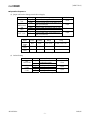
EXT(24 pin Header) Pin Layout
Pin No. Name I/O Function
1 EXT-BCLK1 I
2 EXT-JX0/BCLK3 I/O
3 EXT-SYNC1 I
4 JX1/SYNC3 I/O
5 EXT-SDIN1 I
6 EXT-SDIN3 I/O
7 EXT-SDOUT1 O
8 EXT-SDOUT3/GP0 I/O
9 EXT-BCLK2 O
10 EXT-SDIN4 I
11 EXT-SYNC2 O
12 EXT-SDOUT4/GP1 I/O
13 EXT-SDIN2 I
14 EXT-STO/RDY O
15 EXT-SDOUT2 O
16 EXT-PDN I/O
These pins are connected to the AK7719
via Buffer Level Shifter
17 EXT-CSN/SCL I/O
This pin is used when controlling the AKD7719 via EXT.
Refer to DIPSW Setting
18 open -
19 EXT-SO/SDA I/O
This pin is used when controlling the AKD7719 via EXT.
Refer to DIPSW Setting
20 GND - GND
21 EXT-SCLK/CAD0 I/O
This pin is used when controlling the AKD7719 via EXT.
Refer to DIPSW Setting
22 EXT-VDD+1.2V O
This pin is used for VDD supply via EXT.
Refer to JP Setting
23 EXT-SI/CAD1 I/O
This pin is used when controlling the AKD7719 via EXT.
Refer to DIPSW Setting
24 EXT-TVDD O
This pin is used for TVDD supply via EXT.
Refer to JP Setting

[AKD7719-A]
<KM107300> 2011/06
- 4 -
■ Control Box
The AKD7719-A should be connected to a PC via an USB control box. The USB control box is connected to a PC with an
USB cable and the AKD7719-A with 10-pin flat cable.
Set jumper pins to select control I/F (I
2
C or SPI).
SPI(Serial) I2C
The switch of I2C labeled on S2 should be set when changing SPI/I2C.
USB
Flat 10pin
open
open
short
shor
t
short
short
open
(default)
open

[AKD7719-A]
<KM107300> 2011/06
- 5 -
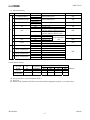
■ Operation Sequence
(1) Jumper and Test Pin Setting (near the Power Supply)
Name Setting Using Default Setting
Open
External TVDD supply on TP1
JP3
3.3V
Short
TVDD = 3.3V fixed
Short
Open
External TVDD supply on the 24pin of J1.
(JP3: not connected)
JP4
EXT-TVDD
Short
EXT-TVDD = TVDD
Open
Open External VDD input supply VDD on TP2JP6
REG
Short VDD+1.2V fixed
Short
Open VDD = JP6(REG)
JP7
EXT-VDD
Short
External VDD supply on the 22pin of J1.
(JP6: not connected)
Open
Table 1. Jumper Pin Setting
Name Color
Typ
Voltage
Voltage
Range
Using
TP1
TVDD
Red +3.3V +1.6~+3.6V TVDD of AK7719
TP2
VDD
Yellow +1.2V +1.1~+1.3V VDD of AK7719
TP3
GND
Black 0V 0V Ground
Table 2. Test Pin Setting
(2) CutLand Setting
Name Setting Using Default Setting
Open
7719-TVDD
independent supply
CL1
7719-TVDD
Short
7719-TVDD = TVDD
Short
Open CAD0 pin = L CL2
CAD0
Short CAD0 pin = H
Open
Open CAD1 pin = L CL3
CAD1
Short CAD1 pin = H
Open
Table 3. CutLand Setting

[AKD7719-A]
<KM107300> 2011/06
- 6 -
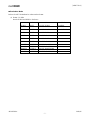
(3) DIP Switch Setting
Name Setting Using Default Setting
OFF(MAIN)
8 7719[MAIN/EXT]
ON(EXT)
Default setting fixed.
OFF
OFF(EXT)
7 MAINIF[EXT/CTRL]
ON(CTRL)
Default setting fixed.
ON
OFF(MAIN)
6 EXTIF[MAIN/CTRL]
ON(CTRL)
Default setting fixed.
OFF
OFF I2C pin = “L”
5 I2C
ON I2C pin = “H”
ON
OFF DIPSW control of JX0/1 for the
AK7719 (MAIN or EXT) is invalid.
4 JXE
ON DIPSW control of JX0/1 for the
AK7719 (MAIN or EXT) is valid.
OFF
OFF JX0 pin = “L”
3 JX0
ON JX0 pin = “H”
OFF
OFF JX1 pin = “L”
2 JX1
ON JX1 pin = “H”
Valid when JXE =
ON
OFF
OFF TEST = “L”
S1
1 TEST
ON TEST = “H”
OFF
OFF PULL-UP OPEN (CSN/SCL)
1 PULL-UP[OFF/ON]
ON PULL-UP (CSN/SCL)
OFF PULL-UP OPEN (SCLK/CAD0)
2 PULL-UP[OFF/ON]
ON PULL-UP (SCLK/CAD0)
OFF PULL-UP OPEN (SO/SDA)
3 PULL-UP[OFF/ON]
ON PULL-UP (SO/SDA)
OFF PULL-UP OPEN (PDN)
S2
4 PULL-UP[OFF/ON]
ON PULL-UP (PDN)
OFF
Table 4. DIPSW Setting
Control Interface Setting
DIP Switch
AK7719 I/F connection
I2C EXTIF MAINIF 7719
I2C CONTROL ON OFF ON
OFF (default)
MAIN
on board
SPI CONTROL OFF
OFF
ON
OFF
EXT *
not on board
I2C CONTROL ON ON ON ON
(*: Used when controlling the AK7719 which is externally connected.)
(4) Set up connectors. ( refer to Evaluation Mode )
(5) Power On.
(6) Run the control software (AK7719.exe) and download the appropriate script file. ( see script section )

[AKD7719-A]
<KM107300> 2011/06
- 7 -
■ Evaluation Mode
Refer to the AK7719 datasheet for audio interface format.
(1) Format : I
2
S 16bit
Provide SYNC1 and BICK1 to the device.
Condition Name Clocks
SYNC1
INPUT
J1-3 EXT-SYNC1 1fs=48kHz
BCLK1
INPUT
J1-1 EXT-BCLK1 64fs=3.072MHz
SDIN1 INPUT J1-5 EXT-SDIN1 -
SDIN2 INPUT J1-13 EXT-SDIN2 -
SDIN3 INPUT J1-6 EXT-SDIN3 -
SDIN4 INPUT J1-10 EXT-SDIN4 -
SDOUT1 OUTPUT J1-7 EXT-SDOUT2 -
SDOUT2 OUTPUT J1-15 EXT-SDOUT2 -
SDOUT3 OUTPUT J1-8 EXT-SDOUT3/GP0 -
SDOUT4 OUTPUT J1-12 EXT-SDOUT4/GP1 -

[AKD7719-A]
<KM107300> 2011/06
- 8 -
CONTROL SOFTWARE MANUAL
■ Setup of the Evaluation Board and Control Software
(1) Power the AKD7719-A-MAIN evaluation board on and connect it with a USB control box.
(2) Connect the USB control box to a PC with a USB cable.
The USB control box will be recognized as HID (Human Interface Device). When it can not be recognized
correctly (e.g., unknown device is connected), please push reset button [yellow] on the USB control box.
(3) Install AK7719.exe to the PC. Then ready to evaluate.
The start-up image of control software is as below.
Figure 3. Start-up Image of Control Software
When the connection of PC with the USB control box is removed, it is required to restart the control software.

[AKD7719-A]
<KM107300> 2011/06
- 9 -
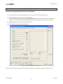
■ Download the DSP Program and Registers Software
1. Register Setting and Code Downloading
1-1. Register Setting
(1) Select the SCRIPT tab to set register values.
(2) “script_7719_test.txt” runs under the condition below.
FSMode11: 48kHz / 16bit Linear / I2S
(1)
(2)
(2) load script file (Example)
File: script_7719_test.txt
After loading the script file,
the AK7719 becomes running state.
Confirm that DSP/Clock block are
powered-up.

[AKD7719-A]
<KM107300> 2011/06
- 10 -
1-2. Code Downloading
There are four code areas as shown below.
Code Area Alias Function
Control Register CONT AK7719 operation mode setup
Program RAM PRAM Storage RAM for program code
Coefficient RAM CRAM Storage RAM for parameter used by program code
Offset Register OFREG Pointer for delay RAM address
Table 5. AK7719 Code Area
(Note 1) All codes (CONT, PRAM, CRAM and OFREG) will be provided by AKM.
(1) Click the download tab and see if the file to be downloaded.
Figure 4. [Download] Dialogue of Control Software
(3) Uncheck the “CRC_Check” box, click the write button to download DSP programs into the AK7719.
If a write error is occurred, check if the clocks are provided to the AK7719.
(4) Confirm Run state of the DSPRSTN button
Now, the AK7719 is in running state. Input signal to the Port#1(SDIN1) is output from SDOUT2, 3 and 4.
SDIN1
AK7719-DSPB
0.5
0.5
Delay(24sample)
SDOUT2
SDOUT3
SDOUT4
Figure 3. Signal Flow
(2) Program, CRAM, OFREG to be
downloaded
PRAM File:
DSP_7719_test.obj
CRAM File
:
DSP_7719_test.cra
OFREG File:
DSP_7719_test.off
(1)
(2)
(4)
(3)

[AKD7719-A]
<KM107300> 2011/06
- 11 -
REVISION HISTORY
IMPORTANT NOTICE
z These products and their specifications are subject to change without notice.
When you consider any use or application of these products, please make inquiries the sales office of Asahi Kasei
Microdevices Corporation (AKM) or authorized distributors as to current status of the products.
z Descriptions of external circuits, application circuits, software and other related information contained in this
document are provided only to illustrate the operation and application examples of the semiconductor products. You
are fully responsible for the incorporation of these external circuits, application circuits, software and other related
information in the design of your equipments. AKM assumes no responsibility for any losses incurred by you or third
parties arising from the use of these information herein. AKM assumes no liability for infringement of any patent,
intellectual property, or other rights in the application or use of such information contained herein.
z Any export of these products, or devices or systems containing them, may require an export license or other official
approval under the law and regulations of the country of export pertaining to customs and tariffs, currency exchange,
or strategic materials.
z AKM products are neither intended nor authorized for use as critical components
Note1)
in any safety, life support, or
other hazard related device or system
Note2)
, and AKM assumes no responsibility for such use, except for the use
approved with the express written consent by Representative Director of AKM. As used here:
Note1) A critical component is one whose failure to function or perform may reasonably be expected to result,
whether directly or indirectly, in the loss of the safety or effectiveness of the device or system containing it, and
which must therefore meet very high standards of performance and reliability.
Note2) A hazard related device or system is one designed or intended for life support or maintenance of safety
or for applications in medicine, aerospace, nuclear energy, or other fields, in which its failure to function or
perform may reasonably be expected to result in loss of life or in significant injury or damage to person or
property.
z It is the responsibility of the buyer or distributor of AKM products, who distributes, disposes of, or otherwise places
the product with a third party, to notify such third party in advance of the above content and conditions, and the buyer
or distributor agrees to assume any and all responsibility and liability for and hold AKM harmless from any and all
claims arising from the use of said product in the absence of such notification.
Date
(yy/mm/dd)
Manual
Revision
Board
Revision
Reason Page Contents
11/06/28 KM107300 0 First edition

5
5
4
4
3
3
2
2
1
1
D D
C C
B B
A A
AKD7719-A-MAIN
TOP
Title
Size Document Number Rev
Date: Sheet
of
0A
17Thursday, August 04, 2011
Title
Size Document Number Rev
Date: Sheet of
0A
17Thursday, August 04, 2011
Title
Size Document Number Rev
Date: Sheet of
0A
17Thursday, August 04, 2011
POWER
POWER
CTRL
CTRL
CTRL-HOST
CTRL-SCK/SCL
CTRL-CSN
CTRL-RQN
CTRL-SI
CTRL-RESET
CTRL-SO
CTRL-XCS/SDA
CTRL-DSP-I2C
EXT
EXT
EXT-SDIN3
EXT-SDIN4
EXT-PDN
EXT-SDOUT3/GP0
EXT-SDOUT4/GP1
EXT-STO/RDY
EXT-BCLK1
EXT-SYNC1
EXT-SDIN1
EXT-SDIN2
EXT-CSN/SCL
EXT-SCLK/CAD0
EXT-SI/CAD1
EXT-SDOUT1
EXT-BCLK2
EXT-SYNC2
EXT-SDOUT2
EXT-SO/SDA
EXT-JX0/BCLK3
EXT-JX1/SYNC3
MONITOR
MONITOR
mon-SDIN3
mon-SDLED
mon-SPDIF
mon-PDN
mon-BICK1
mon-SYNC1
AK7719
AK7719
AK7719-I2C
AK7719-SCLK/CAD0
AK7719-SI/CAD1
AK7719-CSN/SCL
AK7719-SO/SDA
AK7719-STO/RDY
AK7719-SYNC2
AK7719-BCLK2
AK7719-SDOUT2
AK7719-SDIN2
AK7719-SDOUT4/GP1
AK7719-SDIN4
AK7719-PDN
AK7719-TEST
AK7719-SYNC1
AK7719-BCLK1
AK7719-SDIN1
AK7719-SDOUT1
AK7719-SDOUT3/GP0
AK7719-SDIN3
AK7719-BUFE
AK7719-JX0/BCLK3
AK7719-JX1/SYNC3
SELECTOR
SELECTOR
SEL-DSP-SO/SDA
SEL-DSP-CSN/SCL
SEL-DSP-SCLK/CAD0
SEL-DSP-SI/CAD1
SEL-DSP-I2C
SEL-DSP-TEST
SEL-EXT-SCLK/CAD0
SEL-EXT-SI/CAD1
SEL-DSP-PDN
SEL-CTRL-RQN
SEL-EXT-PDN
SEL-CTRL-SI
SEL-CTRL-RESET
SEL-EXT-CSN/SCL
SEL-EXT-SO/SDA
SEL-CTRL-SCK/SCL
SEL-CTRL-XCS/SDA
SEL-CTRL-SO
SEL-DSP-BUFE
SEL-EXT-JX1/SYNC3
SEL-DSP-JX0/BCLK3
SEL-DSP-JX1/SYNC3
SEL-EXT-JX0/BCLK3

5
5
4
4
3
3
2
2
1
1
D D
C C
B B
A A
AKD7719-A-MAIN
AK7719
DSP-JX1/SYNC3
DSP-SDOUT4/GP1
DSP-SDIN1
DSP-TEST
DSP-PDN
DSP-JX0/BCLK3
DSP-SDOUT1
DSP-SDIN3DSP-STO/RDY
DSP-SDIN2
DSP-BCLK2
DSP-SDOUT2
DSP-I2C
DSP-SDIN4
DSP-SDOUT3/GP0
DSP-STO/RDY
DSP-SDOUT4/GP1
DSP-SDOUT1
DSP-SYNC2
DSP-BCLK2
DSP-SDOUT2
DSP-JX1/SYNC3
DSP-JX0/BCLK3
DSP-SDIN3
DSP-SDIN4
DSP-BCLK1
DSP-SYNC1
DSP-SDIN1
DSP-I2C
DSP-PDN
DSP-TEST
DSP-SDIN2
DSP-SDOUT3/GP0
DSP-SYNC2
DSP-BCLK1
DSP-SYNC1
DSP-SYNC2
DSP-STO/RDY
DSP-BCLK2
DSP-SDIN3
DSP-SDOUT2
DSP-SDOUT4/GP1
DSP-JX0/BCLK3
DSP-SDOUT3/GP0
DSP-PDN
DSP-JX1/SYNC3
DSP-SDIN4
DSP-TEST
DSP-SDIN2
DSP-SYNC1
AK7719-SI/CAD1
AK7719-SCLK/CAD0
DSP-I2C
DSP-BCLK1
DSP-SDIN1
AK7719-SO/SDA
AK7719-CSN/SCL
DSP-SDOUT1
AK7719-I2C
AK7719-SDIN2
AK7719-SDIN4
AK7719-PDN
AK7719-TEST
AK7719-SYNC1
AK7719-BCLK1
AK7719-SDIN1
AK7719-JX0/BCLK3
AK7719-JX1/SYNC3
AK7719-SDIN3
AK7719-BUFE
AK7719-STO/RDY
AK7719-SYNC2
AK7719-BCLK2
AK7719-SDOUT2
AK7719-SDOUT1
AK7719-SDOUT3/GP0
AK7719-SDOUT4/GP1
AK7719-SO/SDA
AK7719-SCLK/CAD0
AK7719-CSN/SCL
AK7719-SI/CAD1
TVDD
7719-TVDD
7719-VDD+1.2V
7719-TVDD
7719-VDD+1.2V
Title
Size Document Number Rev
Date: Sheet
of
0B
27Thursday, August 04, 2011
Title
Size Document Number Rev
Date: Sheet
of
0B
27Thursday, August 04, 2011
Title
Size Document Number Rev
Date: Sheet
of
0B
27Thursday, August 04, 2011
R8 51
CN2
28pin_R
15
16
17
18
19
20
21
22
23
24
25
26
27
28
R9 51
R1 51
R3 51
R10 51
R17 51
R18 51
C2
0.1uF
R16 51
R15 51
R14 51
R2 51
R13 51
U1AK7719
SYNC1
E5
BCLK1
D5
SDIN1
B5
SDOUT1
C5
JX1/SYNC3
B3
JX0/BCLK3
B4
SDIN3
C4
SDOUT3/GP0
D4
PDN
A5
VSS
A3
VDD
A4
TVDD
A2
SYNC2
E4
BCLK2
E3
SDOUT2
E1
SDIN2
E2
SDOUT4/GP1
D2
SDIN4
C2
STO/RDY
D3
I2C
B2
SCLK/CAD0
B1
SI/CAD1
A1
CSN/SCL
C1
SO/SDA
D1
TEST
C3
C6
0.1uF
R12 51
R11 51
R20 0
U2
SN74ALVCH16827
1OE1
1
1OE2
56
2OE1
28
2OE2
29
1Y1
2
1Y2
3
1Y3
5
1Y4
6
GND
4
GND
11
GND
18
GND
25
GND
32
GND
39
GND
46
GND
53
VCC
7
VCC
22
VCC
35
VCC
50
1Y8
12
1Y9
13
1Y10
14
2Y1
15
2Y2
16
2Y3
17
2Y4
19
2Y5
20
2Y6
21
2Y7
23
2Y8
24
2Y9
26
2Y10
27
2A10
30
2A9
31
2A1
42
2A2
41
2A3
40
2A4
38
2A5
37
2A6
36
2A7
34
2A8
33
1A1
55
1A2
54
1A3
52
1A4
51
1A5
49
1A6
48
1A7
47
1A8
45
1A9
44
1A10
43
1Y5
8
1Y6
9
1Y7
10
R22 0
R19 0
R21 0
CN1
28pin_L
1
2
3
4
5
6
7
8
9
10
11
12
13
14
C4
0.1uF
C1
0.1uF
R4 51
R5 51
C5
4.7uF
R6 51
R7 51
C3
0.1uF
Page is loading ...

5
5
4
4
3
3
2
2
1
1
D D
C C
B B
A A
AKD7719-A-MAIN
EXT
TEST
EXT
EXT-SDIN4
EXT-STO/RDY
EXT-BCLK1
EXT-SYNC1
EXT-SDIN1
EXT-SDIN2
EXT-SDOUT1
EXT-BCLK2
EXT-SYNC2
EXT-SDOUT2
EXT-SO/SDA
EXT-SDOUT3/GP0
EXT-SDOUT4/GP1
EXT-PDN
EXT-CSN/SCL
EXT-SCLK/CAD0
EXT-SI/CAD1
EXT-JX0/BCLK3
EXT-JX1/SYNC3
EXT-SDIN3
EXT-TVDD
EXT-VDD+1.2V
Title
Size Document Number Rev
Date: Sheet
of
0A
47Thursday, August 04, 2011
Title
Size Document Number Rev
Date: Sheet of
0A
47Thursday, August 04, 2011
Title
Size Document Number Rev
Date: Sheet of
0A
47Thursday, August 04, 2011
R59 51
R56 51
R61 51
R55 51
R52 51
J2
HEADER 14X2
2
4
6
8
10
12
14
16
18
20
22
24
26
28
1
3
5
7
9
11
13
15
17
19
21
23
25
27
C15
0.1uF
R58 51
C14
0.1uF
R50 51
R53 51
J1
HEADER 12X2
2
4
6
8
10
12
14
16
18
20
22
24
1
3
5
7
9
11
13
15
17
19
21
23
R57 51
R60 51
R51 51
R54 51
R49 51

5
5
4
4
3
3
2
2
1
1
D D
C C
B B
A A
MONITOR
AKD7719-A-MAIN
MONITOR
BICK1
SYNC1
PDN
SDO-SPDIF
SDO-LED
mon-SDIN3
mon-SDLED
mon-SPDIF
mon-BICK1
mon-SYNC1
mon-PDN
VDD+3.3VEXT-TVDD
EXT-TVDD VDD+3.3V
VDD+3.3V
Title
Size Document Number Rev
Date: Sheet
of
0A
57Thursday, August 04, 2011
Title
Size Document Number Rev
Date: Sheet of
0A
57Thursday, August 04, 2011
Title
Size Document Number Rev
Date: Sheet of
0A
57Thursday, August 04, 2011
C19
0.1uF
R64 51
U6
SN74AVC8T245PW
A1
3
A2
4
A3
5
A4
6
A5
7
A6
8
A7
9
A8
10
B1
21
B2
20
B3
19
B4
18
B5
17
B6
16
B7
15
B8
14
VCCB
23
VCCB
24
GND
12
OEN
22
GND
13
VCCA
1
DIR
2
GND
11
C20
0.1uF
R62 51
R67 51
R63 51
JP2
HEADER 5X2
1 2
3 4
5 6
7 8
9 10
C18
0.1uF
R66 51
C16
0.1uF
C17
0.1uF
R65 51
U7A
SN74AVCH1T45DCK
VCCA
1
GND
2
A
3
B
4
DIR
5
VCCB
6

5
5
4
4
3
3
2
2
1
1
D D
C C
B B
A A
3.3V
3.3V
REG
AKD7719-A-MAIN
POWER
TVDD
VDD
EXT-TVDD
EXT-VDD
REG+1.2V
TVDDVDD+3.3V
7719-TVDD
EXT-TVDD
7719-VDD+1.2V
EXT-VDD+1.2V
Title
Size Document Number Rev
Date: Sheet
of
0A
67Thursday, August 04, 2011
Title
Size Document Number Rev
Date: Sheet of
0A
67Thursday, August 04, 2011
Title
Size Document Number Rev
Date: Sheet of
0A
67Thursday, August 04, 2011
REG1
XC6210B-1.2
IN
1
CE
3
OUT
5
NC
4
GND
2
TP3
BLACK
1
+
C23
10uF
JP6
JMP2_1
JP4
JMP2_1
JP5
HEADER 2
1
2
+
C21
10uF/16V(A)
TP2
YELLOW
1
JP3
JMP2_1
C22
1.0uF
CL1
Cut Land short
1 2
C24
0.1uF
TP1
RED
1
JP7
JMP2_1

5
5
4
4
3
3
2
2
1
1
D D
C C
B B
A A
7719[MAIN/EXT]
MAINIF[EXT/CTRL]
EXTIF[MAIN/CTRL]
I2C
JXE
JX0
JX1
TEST
AKD7719-A-MAIN
SELECTOR
PULL-UP[OFF/ON]
CAD0
CAD1
CTRL-SDA
CTRL-SCL
EXT-SDA
EXT-SCL
PDN
SDA
SCLK
SCL
DIP-MAINIF
DIP-JX1
DIP-JX0
DIP-JXE
DIP-MAINIF
DIP-EXTIF
DIP-EXTIF
DIP-EXTIF
DIP-MAINIF
SEL-DSP-I2C
IF-CTRL-SO/SDA
IF-EXT-CSN/SCL
IF-EXT-SCLK/CAD0
IF-CTRL-SCLK/CAD0
IF-EXT-SI/CAD1
IF-EXT-SO/SDA
IF-CTRL-SI/CAD1
IF-CTRL-CSN/SCL
IF-CTRL-SO/SDA
IF-CAD0
IF-CAD1
IF-CAD0
IF-CAD1
IF-CAD0
IF-CAD1
SEL-DSP-I2C
DIP-JX1
DIP-JXE
DIP-JX0
SEL-DSP-JX0/BCLK3
SEL-DSP-JX1/SYNC3
SEL-DSP-SO/SDA
SEL-DSP-CSN/SCL
SEL-DSP-SCLK/CAD0
SEL-DSP-SI/CAD1
SEL-DSP-I2C
SEL-DSP-TEST
SEL-DSP-PDN
SEL-CTRL-RQN
SEL-CTRL-SI
SEL-CTRL-RESET
SEL-EXT-SO/SDA
SEL-CTRL-SCK/SCL
SEL-CTRL-XCS/SDA
SEL-CTRL-SO
SEL-DSP-BUFE
SEL-EXT-CSN/SCL
SEL-EXT-PDN
SEL-EXT-JX0/BCLK3
SEL-EXT-JX1/SYNC3
SEL-EXT-SCLK/CAD0
SEL-EXT-SI/CAD1
TVDD
TVDD
TVDD
TVDD
TVDD
TVDD
TVDD
TVDD
TVDD
TVDD
Title
Size Document Number Rev
Date: Sheet
of
0B
77Thursday, August 04, 2011
Title
Size Document Number Rev
Date: Sheet
of
0B
77Thursday, August 04, 2011
Title
Size Document Number Rev
Date: Sheet
of
0B
77Thursday, August 04, 2011
R79 0
R76 4.7k
R82
10k
C31
0.1uF
R86
Dip10k
C28
0.1uF
C26
0.1uF
C29
0.1uF
U8
TS3A44159PW
NC1
15
NO1
13
NC2
3
NO2
1
IN1-2
16
NC3
7
NO3
5
NC4
11
NO4
9
IN3-4
8
GND
4
V+
12
COM4
10
COM3
6
COM2
2
COM1
14
U14 PACK8-10k
1
2
3
4
5
6
7
8
9
R85
Dip10k
U10
TS3A44159PW
NC1
15
NO1
13
NC2
3
NO2
1
IN1-2
16
NC3
7
NO3
5
NC4
11
NO4
9
IN3-4
8
GND
4
V+
12
COM4
10
COM3
6
COM2
2
COM1
14
U11
TS3A44159PW
NC1
15
NO1
13
NC2
3
NO2
1
IN1-2
16
NC3
7
NO3
5
NC4
11
NO4
9
IN3-4
8
GND
4
V+
12
COM4
10
COM3
6
COM2
2
COM1
14
S1
SW DIP-4
1
2
3
4
8
7
6
5
TP6
LBLUE
1
TP5
WHITE
1
C25
0.1uF
TP7
WHITE
1
R75 4.7k
R68 0
CL3
Cut Land open
12
R72 0
U9
TS5A23159DGS
NC1
9
NO1
2
IN1
1
NC2
7
NO2
4
IN2
5
GND
3
V+
8
COM2
6
COM1
10
R77 0
C27
0.1uF
R80 0
R78 4.7k
R71
10k
U12
TS5A23159DGS
NC1
9
NO1
2
IN1
1
NC2
7
NO2
4
IN2
5
GND
3
V+
8
COM2
6
COM1
10
R73 10k
CL2
Cut Land open
12
R81
10k
C30
0.1uF
R70
10k
S2
SW DIP-8
1
2
3
4
5
6
7
8
16
15
14
13
12
11
10
9
U13
TS3A44159PW
NC1
15
NO1
13
NC2
3
NO2
1
IN1-2
16
NC3
7
NO3
5
NC4
11
NO4
9
IN3-4
8
GND
4
V+
12
COM4
10
COM3
6
COM2
2
COM1
14
U15
TS5A3159
NC
3
NO
1
IN
6
GND
2
V+
5
COM
4
R69 0
R74 0
TP4
LBLUE
1
-
 1
1
-
 2
2
-
 3
3
-
 4
4
-
 5
5
-
 6
6
-
 7
7
-
 8
8
-
 9
9
-
 10
10
-
 11
11
-
 12
12
-
 13
13
-
 14
14
-
 15
15
-
 16
16
-
 17
17
-
 18
18


Ask a question and I''ll find the answer in the document
Finding information in a document is now easier with AI
Related papers
-
AKM AK4679EG Evaluation Board Manual
-
-
-
-
-
-
-
-
-
Other documents
-
 Asahi KASEI AK9720 User Instruction
-
Cypress Semiconductor CY3655-EXT enCoRe II Quick start guide
-
 MIXX JX1 User Guides
-
Gianni Industries CP-33G Installation guide
-
-
-
 DANLERS MW6A2C IP67 Installation guide
-
AAT KDH-KZ6000FR-IP Quick start guide
-
Fisher & Paykel CAD148E User guide
-
Renishaw NC4 Installation guide


