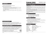
Page is loading ...

[AKD7719B-A]
<KM113201> 2015/08
GENERAL DESCRIPTION
The AKD7719B-A is an evaluation kit for the AK7719B; a digital signal processor (DSP) with digital interface
ports. The built-in asynchronous sample rate converters (SRC) enable flexible connectivity in various system
configurations. It realizes an easy evaluation of the audio system by just connecting to the target product via
digital input and output pins. A USB connection is adopted for control interface, enabling to develop DSP codes
with a PC.
■ Ordering Guide
AKD7719B-A --- Evaluation board for AK7719B
(Main-board:AKD7719B-A-MAIN , Sub-board:AKD7719B-A-SUB)
USB Control Box
Control Software
FUNCTION
Write/Read RAM: Access to PRAM, CRAM, OFFRAM and Registers
Digital Audio Interface
- Test pin header
SDIN
SDOUT
1.2V
AKM
DSP
Core
uPI/F
Regulator
TP3(GND)=0V
Reset
AK7719B
PCM
I/F
I2C or SPI
JP5(TVDD)=3.3V
Device
PCM
I/F
Device
AKD7719B-A-MAIN + AKD7719B-A-SUB
Figure 1. AKD7719B-A Block Diagram
AK7719B Evaluation Board Rev.1
- 1-

[AKD7719B-A]
<KM113201> 2015/08
EVALUATION BORAD
■ Board View
AKD7719B-A-MAIN + AKD7719B-A-SUB
Figure 2. AKD7719B-A Board View
(1)
(2)
(5)
(
7
)
(6)
(4)
(3)
AK7719B
AKD7719B-A-MAIN
(9)
(8)
AKD7719B-A-SUB
- 2-

[AKD7719B-A]
<KM113201> 2015/08
■ Description
AKD7719B-A-MAIN
No. Name Function
(1)
EXT (J1)
(24 pin Header)
External System Signal Connector.
(2) 3.3V (JP5) 3.3V Power Supply Terminal. Use attached connection cable.
(3)
TEST (J2)
(28 pin Header)
External System Connector
(4) Jumper (JP3, JP4, JP6, JP7) Power Supply Select Jumper
(5) DIP Switch (S1, S2) Pin and Signal Select Switches
(6)
MONITOR (JP2)
(10 pin Header)
AKD77XX-HFS MONITOR Board Connector. (for HF Tuning)
(7)
CONTROL (JP1)
(10 pin Header)
USB Control Box Connector
(8)
TEST (TP02-TP28)
( Test pin Header)
External System Connector and Monitor Pin (on Sub-Board)
(9)
EXT (J101)
(20 pin Header)
External System Connector (on Sub-Board)
AKD7719B-A-MAIN
EXT(24 / 27 pin Header) Pin Layout
・24pin Pin Header [ J1 ] :
Pin No. Name I/O Function
1 EXT-BCLK1 I
These pins are connected to the AK7719B
via Buffer Level Shifter
2 EXT-JX0/BCLK3 I/O
3 EXT-SYNC1 I
4 EXT-JX1/SYNC3 I/O
5 EXT-SDIN1 I
6 EXT-SDIN3 I/O
7 EXT-SDOUT1 O
8 EXT-SDOUT3/GP0 I/O
9 EXT-BCLK2 O
10 EXT-SDIN4 I
11 EXT-SYNC2 O
12 EXT-SDOUT4/GP1 I/O
13 EXT-SDIN2 I
14 EXT-STO/RDY O
15 EXT-SDOUT2 O
16 EXT-PDN I/O
17 EXT-CSN/SCL I/O
This pin is used when controlling the AK7719B via EXT.
Refer to DIPSW Setting
18 open -
19 EXT-SO/SDA I/O
This pin is used when controlling the AK7719B via EXT.
Refer to DIPSW Setting
20 GND - GND
21 EXT-SCLK/CAD0 I/O
This pin is used when controlling the AK7719B via EXT.
Refer to DIPSW Setting
22 EXT-VDD+1.2V O
This pin is used for VDD supply via EXT.
Refer to JP Setting
23 EXT-SI/CAD1 I/O
This pin is used when controlling the AK7719B via EXT.
Refer to DIPSW Setting
24 EXT-TVDD O
This pin is used for TVDD supply via EXT.
Refer to JP Setting
- 3-

[AKD7719B-A]
<KM113201> 2015/08
・27pin Pin Header [ J2 ] :
Pin No. Name I/O Function
1 EXT-BCLK1 I
These pins are connected to the AK7719B
via Buffer Level Shifter
2 GND -
3 EXT-SYNC1 I
4 GND -
5 EXT-SDIN1 I
6 GND -
7 EXT-SDOUT1 O
8 GND -
9 EXT-BCLK2 O
10 GND -
11 EXT-SYNC2 O
12 GND -
13 EXT-SDIN2 I
14 GND -
15 EXT-SDOUT2 O
16 GND -
17 EXT-JX0/BCLK3 I/O
18 GND -
19 EXT-JX1/SYNC3 I/O
20 GND -
21 EXT-SDIN3 I/O
22 GND -
23 EXT-SDOUT3/GP0 I/O
24 GND -
25 EXT-SDIN4 I
26 GND -
27 EXT-SDOUT4/GP1 I/O
AKD7719B-A-SUB (AKD7719B-A-30CSP-SUB)
EXT(20pin Header) Pin / TEST Pin Layout
・20pin Pin Header [ J101 ] :
Pin No. Name I/O Function
1 SYNC2-I I
These pins are connected to the AK7719B.
2 GND -
3 BCLK2-I I
4 GND -
5 SYNC4-I I
6 GND -
7 BCLK4-I I
8 GND -
9 SYNC5-O O
10 GND -
11 SYNC5-I I
12 GND -
13 BCLK5-O O
14 GND -
15 BCLK5-I I
16 GND -
17 SDIN5-I I
18 GND -
19 SDOUT5-O O
20 GND -
- 4-

[AKD7719B-A]
<KM113201> 2015/08
・TEST Pin Header [ TP02 – TP28] :
Pin No. Name I/O Function
02 SYNC3/JX1-I I
These pins are connected to the AK7719B.
03 SDIN2-I I
04 TVDD -
05 SDIN4-I I
06 SDOUT2-O O
07 SO/SDA-IO I/O
08 SCLK/CAD0-I I
10 CSN/SCL-I I
11 SI/CAD1-I I
12 I2C-I I
13
SDOUT4/GP1/STO
/RDY-O
O
14 TEST-I I
15 VSS -
16 BCLK2-O O
17 BCLK3/JX0-I I
18 VDD -
19 SYNC1-I I
21 BCLK1-I I
22 PDN-I I
23 SDIN1-I I
25 SDOUT1-O O
26 SYNC2-O O
27 SDOUT3/GP0-O O
28 SDIN3-I I
- 5-

[AKD7719B-A]
<KM113201> 2015/08
■ Control Box
The AKD7719B-A should be connected to a PC via an USB control box. The USB control box is connected to a PC with
an USB cable and the AKD7719B-A with 10-pin flat cable.
Set jumper pins to select control I/F (I2C or SPI).
SPI(Serial) I2C
The switch of I2C labeled on S2 should be set when changing SPI/I2C.
USB
Flat 10pin
open
open
short
short
short
short
open
(default)
open
- 6-

[AKD7719B-A]
<KM113201> 2015/08
■ Operation Sequence
AKD7719B-A-MAIN
(1) Jumper and Test Pin Setting (near the Power Supply)
Name Setting Using Default Setting
JP3
3.3V
Open
External TVDD supply on TP1
Short
Short
TVDD = 3.3V fixed
JP4
EXT-TVDD
Open
External TVDD supply on the 24pin of J1.
(JP3: not connected) Open
Short
EXT-TVDD = TVDD
JP6
REG
Open
External VDD input supply VDD on TP2
Short
Short
VDD+1.2V fixed
JP7
EXT-VDD
Open
VDD = JP6(REG)
Open
Short
External VDD supply on the 22pin of J1.
(JP6: not connected)
Table 1. Jumper Pin Setting
Name Color
Typ
Voltage
Voltage
Range
Using
TP1
TVDD
Red +3.3V +1.6~+3.6V TVDD of AK7719
TP2
VDD
Yellow +1.2V +1.1~+1.3V VDD of AK7719
TP3
GND
Black 0V 0V Ground
Table 2. Test Pin Setting
(2) CutLand Setting
Name Setting Using Default Setting
CL1
7719-TVDD
Open
7719-TVDD
independent supply
Short
Short
7719-TVDD = TVDD
CL2
CAD0
Open
CAD0 pin = L
Open
Short
CAD0 pin = H
CL3
CAD1
Open
CAD1 pin = L
Open
Short
CAD1 pin = H
Table 3. CutLand Setting
- 7-

[AKD7719B-A]
<KM113201> 2015/08
(3) DIP Switch Setting
Name Setting Using Default Setting
S1
8 7719[MAIN/EXT]
OFF(MAIN)
Default setting fixed.
OFF
ON(EXT)
7 MAINIF[EXT/CTRL]
OFF(EXT)
Default setting fixed.
ON
ON(CTRL)
6 EXTIF[MAIN/CTRL]
O
FF(MAIN)
Default setting fixed.
OFF
ON(CTRL)
5 I2C
OF
F
I2C pin =
“
L
”
OFF
ON
I2C pin =
“
H
”
4 JXE
OFF
DIPSW control of JX0/1 for the
AK7719B(MAIN or EXT) is invalid.
OFF
ON
DIPSW control of JX0/1 for the
AK7719B(MAIN or EXT) is valid.
3 JX0
OFF
JX0 pin =
“
L
”
Valid when JXE =
ON
OFF
ON
JX0
pin =
“
H
”
2 JX1
OFF
JX1 pin =
“
L
”
OFF
ON
JX1 pin =
“
H
”
1 TEST
OFF
TEST =
“
L
”
OFF
ON
TEST =
“
H
”
S2
1 PULL-UP[OFF/ON]
OFF
PULL
-
UP OPEN (CSN/SCL)
OFF
ON
PULL
-
UP (CSN/SCL)
2 PULL-UP[OFF/ON]
OFF
PULL
-
UP OPEN (SCLK/CAD0)
ON
PULL
-
UP
(SCLK/CAD0)
3 PULL-UP[OFF/ON]
OFF
PULL
-
UP OPEN (SO/SDA)
ON
PULL
-
UP (SO/SDA)
4 PULL-UP[OFF/ON]
OFF
PULL
-
UP OPEN (PDN)
ON
PULL
-
UP (PDN)
Table 4. DIPSW Setting
Control Interface Setting
AK7719B I/F connection
DIP Switch
I2C
EXTIF
MA
INIF
7719
MAIN
on board
I2C
CONTROL
ON
OFF
ON
OFF
SPI
CONTROL
OFF
OFF
ON
OFF (default)
EXT
*
not on board
I2C
CONTROL
ON
ON
ON
ON
(*: Used when controlling the AK7719B which is externally connected.)
(4) Set up connectors. ( refer to Evaluation Mode )
(5) Power On.
(6) Run the control software (AK7719B.exe) and download the appropriate script file. ( see script section )
- 8-

[AKD7719B-A]
<KM113201> 2015/08
■ Evaluation Mode
Refer to the AK7719B datasheet for audio interface format.
(1) Evaluation Port : Port#1 to Port#2 and Port#2 to Port#1
Format : fs=8kHz, BCLK=64fs, I
2
S 16bit data
Condition Name Clocks
SYNC1 INPUT J2-3 EXT-SYNC1 1fs=8kHz
BCLK1 INPUT J2-1 EXT-BCLK1 64fs=512kHz
SDIN1 INPUT J2-5 EXT-SDIN1 I
2
S, 16bit data
SDOUT1 OUTPUT J2-7 EXT-SDOUT1 Data Monitor
SYNC2 INPUT Sub J101-1 SYNC2 1fs=8kHz
BCLK2 INPUT Sub J101-3 BCLK2 64fs=512kHz
SDIN2 INPUT J2-13 EXT-SDIN2 I
2
S, 16bit data
SDOUT2 OUTPUT J2-15 EXT-SDOUT2 Data Monitor
SYNC3 INPUT Sub TP02 SYNC3 -
BCLK3 INPUT Sub TP17 BCLK3 -
SDIN3 INPUT Sub TP28 SDIN3 -
SDOUT3 OUTPUT Sub TP27 SDOUT3 -
SYNC4 INPUT Sub J101-5 SYNC4 -
BCLK4 INPUT Sub J101-7 BCLK4 -
SDIN4 INPUT J2-25 EXT-SDIN4 -
SDOUT4 OUTPUT J2-27 EXT-SDOUT4 -
SYNC5 INPUT Sub J101-11 SYNC5 -
BCLK5 INPUT Sub J101-15 BCLK5 -
SDIN5 INPUT Sub J101-17 SDIN5 -
SDOUT5 OUTPUT Sub J101-J19 SDOUT5 -
(2) Evaluation Port : Port#1 to Port#3 and Port#3 to Port#1
Format : fs=8kHz, BCLK=64fs, I
2
S 16bit data
Condition Name Clocks
SYNC1 INPUT J2-3 EXT-SYNC1 1fs=8kHz
BCLK1 INPUT J2-1 EXT-BCLK1 64fs=512kHz
SDIN1 INPUT J2-5 EXT-SDIN1 I
2
S, 16bit data
SDOUT1 OUTPUT J2-7 EXT-SDOUT1 Data Monitor
SYNC2 INPUT Sub J101-1 SYNC2 -
BCLK2 INPUT Sub J101-3 BCLK2 -
SDIN2 INPUT J2-13 EXT-SDIN2 -
SDOUT2 OUTPUT J2-15 EXT-SDOUT2 -
SYNC3 INPUT Sub TP02 SYNC3 1fs=8kHz
BCLK3 INPUT Sub TP17 BCLK3 64fs=512kHz
SDIN3 INPUT Sub TP28 SDIN3 I
2
S, 16bit data
SDOUT3 OUTPUT Sub TP27 SDOUT3 Data Monitor
SYNC4 INPUT Sub J101-5 SYNC4 -
BCLK4 INPUT Sub J101-7 BCLK4 -
SDIN4 INPUT J2-25 EXT-SDIN4 -
SDOUT4 OUTPUT J2-27 EXT-SDOUT4 -
SYNC5 INPUT Sub J101-11 SYNC5 -
BCLK5 INPUT Sub J101-15 BCLK5 -
SDIN5 INPUT Sub J101-17 SDIN5 -
SDOUT5 OUTPUT Sub J101-J19 SDOUT5 -
- 9-

[AKD7719B-A]
<KM113201> 2015/08
(3) Evaluation Port : Port#1 to Port#4 and Port#4 to Port#1
Format : fs=8kHz, BCLK=64fs, I
2
S 16bit data
Condition Name Clocks
SYNC1 INPUT J2-3 EXT-SYNC1 1fs=8kHz
BCLK1 INPUT J2-1 EXT-BCLK1 64fs=512kHz
SDIN1 INPUT J2-5 EXT-SDIN1 I
2
S, 16bit data
SDOUT1 OUTPUT J2-7 EXT-SDOUT1 Data Monitor
SYNC2 INPUT Sub J101-1 SYNC2 -
BCLK2 INPUT Sub J101-3 BCLK2 -
SDIN2 INPUT J2-13 EXT-SDIN2 -
SDOUT2 OUTPUT J2-15 EXT-SDOUT2 -
SYNC3 INPUT Sub TP02 SYNC3 -
BCLK3 INPUT Sub TP17 BCLK3 -
SDIN3 INPUT Sub TP28 SDIN3 -
SDOUT3 OUTPUT Sub TP27 SDOUT3 -
SYNC4 INPUT Sub J101-5 SYNC4 1fs=8kHz
BCLK4 INPUT Sub J101-7 BCLK4 64fs=512kHz
SDIN4 INPUT J2-25 EXT-SDIN4 I
2
S, 16bit data
SDOUT4 OUTPUT J2-27 EXT-SDOUT4 Data Monitor
SYNC5 INPUT Sub J101-11 SYNC5 -
BCLK5 INPUT Sub J101-15 BCLK5 -
SDIN5 INPUT Sub J101-17 SDIN5 -
SDOUT5 OUTPUT Sub J101-J19 SDOUT5 -
(4) Evaluation Port : Port#1 to Port#5 and Port#5 to Port#1
Format : fs=8kHz, BCLK=64fs, I
2
S 16bit data
Condition Name Clocks
SYNC1 INPUT J2-3 EXT-SYNC1 1fs=8kHz
BCLK1 INPUT J2-1 EXT-BCLK1 64fs=512kHz
SDIN1 INPUT J2-5 EXT-SDIN1 I
2
S, 16bit data
SDOUT1 OUTPUT J2-7 EXT-SDOUT1 Data Monitor
SYNC2 INPUT Sub J101-1 SYNC2 -
BCLK2 INPUT Sub J101-3 BCLK2 -
SDIN2 INPUT J2-13 EXT-SDIN2 -
SDOUT2 OUTPUT J2-15 EXT-SDOUT2 -
SYNC3 INPUT Sub TP02 SYNC3 -
BCLK3 INPUT Sub TP17 BCLK3 -
SDIN3 INPUT Sub TP28 SDIN3 -
SDOUT3 OUTPUT Sub TP27 SDOUT3 -
SYNC4 INPUT Sub J101-5 SYNC4 -
BCLK4 INPUT Sub J101-7 BCLK4 -
SDIN4 INPUT J2-25 EXT-SDIN4 -
SDOUT4 OUTPUT J2-27 EXT-SDOUT4 -
SYNC5 INPUT Sub J101-11 SYNC5 1fs=8kHz
BCLK5 INPUT Sub J101-15 BCLK5 64fs=512kHz
SDIN5 INPUT Sub J101-17 SDIN5 I
2
S, 16bit data
SDOUT5 OUTPUT Sub J101-J19 SDOUT5 Data Monitor
- 10-

[AKD7719B-A]
<KM113201> 2015/08
(5) Evaluation Port : Port#1 to Port#2 and Port#2 to Port#1, Port2=Master
Format : fs=8kHz, BCLK=64fs, I
2
S 16bit data
Condition Name Clocks
SYNC1 INPUT J2-3 EXT-SYNC1 1fs=8kHz
BCLK1 INPUT J2-1 EXT-BCLK1 64fs=512kHz
SDIN1 INPUT J2-5 EXT-SDIN1 I
2
S, 16bit data
SDOUT1 OUTPUT J2-7 EXT-SDOUT1 Data Monitor
SYNC2 OUTPUT Sub J101-1 SYNC2 SYNC Monitor
BCLK2 OUTPUT Sub J101-3 BCLK2 BCLK Monitor
SDIN2 INPUT J2-13 EXT-SDIN2 I
2
S, 16bit data
SDOUT2 OUTPUT J2-15 EXT-SDOUT2 Data Monitor
SYNC3 INPUT Sub TP02 SYNC3 -
BCLK3 INPUT Sub TP17 BCLK3 -
SDIN3 INPUT Sub TP28 SDIN3 -
SDOUT3 OUTPUT Sub TP27 SDOUT3 -
SYNC4 INPUT Sub J101-5 SYNC4 -
BCLK4 INPUT Sub J101-7 BCLK4 -
SDIN4 INPUT J2-25 EXT-SDIN4 -
SDOUT4 OUTPUT J2-27 EXT-SDOUT4 -
SYNC5 INPUT Sub J101-11 SYNC5 -
BCLK5 INPUT Sub J101-15 BCLK5 -
SDIN5 INPUT Sub J101-17 SDIN5 -
SDOUT5 OUTPUT Sub J101-J19 SDOUT5 -
(6) Evaluation Port : Port#1 to Port#5 and Port#5 to Port#1, Port5=Master
Format : fs=8kHz, BCLK=64fs, I
2
S 16bit data
Condition Name Clocks
SYNC1 INPUT J2-3 EXT-SYNC1 1fs=8kHz
BCLK1 INPUT J2-1 EXT-BCLK1 64fs=512kHz
SDIN1 INPUT J2-5 EXT-SDIN1 I
2
S, 16bit data
SDOUT1 OUTPUT J2-7 EXT-SDOUT1 Data Monitor
SYNC2 INPUT Sub J101-1 SYNC2 -
BCLK2 INPUT Sub J101-3 BCLK2 -
SDIN2 INPUT J2-13 EXT-SDIN2 -
SDOUT2 OUTPUT J2-15 EXT-SDOUT2 -
SYNC3 INPUT Sub TP02 SYNC3 -
BCLK3 INPUT Sub TP17 BCLK3 -
SDIN3 INPUT Sub TP28 SDIN3 -
SDOUT3 OUTPUT Sub TP27 SDOUT3 -
SYNC4 INPUT Sub J101-5 SYNC4 -
BCLK4 INPUT Sub J101-7 BCLK4 -
SDIN4 INPUT J2-25 EXT-SDIN4 -
SDOUT4 OUTPUT J2-27 EXT-SDOUT4 -
SYNC5 OUTPUT Sub J101-11 SYNC5 SYNC Monitor
BCLK5 OUTPUT Sub J101-15 BCLK5 BCLK Monitor
SDIN5 INPUT Sub J101-17 SDIN5 I
2
S, 16bit data
SDOUT5 OUTPUT Sub J101-J19 SDOUT5 Data Monitor
- 11-

[AKD7719B-A]
<KM113201> 2015/08
CONTROL SOFTWARE MANUAL
■ Setup of the Evaluation Board and Control Software
(1) Power the AKD7719B-A evaluation board on and connect it with a USB control box.
(2) Connect the USB control box to a PC with a USB cable.
The USB control box will be recognized as HID (Human Interface Device). When it can not be recognized
correctly (e.g., unknown device is connected), please push reset button [yellow] on the USB control box.
(3) Install AK7719B.exe to the PC. Then ready to evaluate.
The start-up image of control software is as below.
Figure 3. Start-up Image of Control Software (AK7719B_A_HF.exe)
(4) Push the “Board Init” button to make sure that this control software access registers. Only if just pushing the “PDN
Pin” button this cannot access the registers.
When the connection of PC with the USB control box is removed, it is required to restart the control software.
- 12-

[AKD7719B-A]
<KM113201> 2015/08
■ Download the DSP Program and Registers Software
1. Register Setting and Code Downloading
1-1. Register Setting
(1) Select the SCRIPT tab to set register values.
(2) “script19B_test.txt” runs under the condition below.
FSMode00: 8kHz / 16bit Linear / I2S
(1)
(2)
(2) load script file
File (Example): script19B_test.txt
(Port#1 to Port#2 and Port#2 to Port#1)
Script File: xxxxx.txt
After loading the script file,
the AK7719B becomes reset state.
Confirm that DSP/Clock block are
powered-down.
- 13-

[AKD7719B-A]
<KM113201> 2015/08
1-2. Code Downloading
There are four code areas as shown below.
Code Area Alias Function
Control Register CONT AK7719B operation mode setup
Program RAM PRAM Storage RAM for program code
Coefficient RAM CRAM Storage RAM for parameter used by program code
Offset Register OFREG Pointer for delay RAM address
Table 5. AK7719B Code Area
(Note 1) All codes (CONT, PRAM, CRAM and OFREG) will be provided by AKM.
(1) Click the DownLoad tab and see if the file to be downloaded.
Figure 4. [Download] Dialogue of Control Software
(3) Check the “CRC_Check” box, click the Write button to download DSP programs into the AK7719B.
If a write error is occurred, check if the clocks are provided to the AK7719B.
(4) Click the DSPRSTN botton. Confirm Run state of the DSPRSTN button
Now, the AK7719B is in running state. Input signal to the Port#1(SDIN1) is output from SDOUT2 or 3 or 4 or 5.
SDIN1
AK7719B DSP&SRC
SDOUT2
SDOUT5
SDOUT4
SRC
SRC
SDOUT3
SRC
DSP
Figure 3. Signal Flow
(2) Program, CRAM, OFREG to be
downloaded
PRAM File (Example): DSP19B_test.obj
(Port#1 to Port#2 and Port#2 to Port#1)
PRAM File: xxxxx.obj
CRAM File: xxxxx.cra
OFREG File: xxxxx.off
(1)
(2)
(4)
A
(3)
- 14-

[AKD7719B-A]
<KM113201> 2015/08
REVISION HISTORY
IMPORTANT NOTICE
0. Asahi Kasei Microdevices Corporation (“AKM”) reserves the right to make changes to the information
contained in this document without notice. When you consider any use or application of AKM product
stipulated in this document (“Product”), please make inquiries the sales office of AKM or authorized
distributors as to current status of the Products.
1. All information included in this document are provided only to illustrate the operation and application
examples of AKM Products. AKM neither makes warranties or representations with respect to the accuracy
or completeness of the information contained in this document nor grants any license to any intellectual
property rights or any other rights of AKM or any third party with respect to the information in this
document. You are fully responsible for use of such information contained in this document in your product
design or applications. AKM ASSUMES NO LIABILITY FOR ANY LOSSES INCURRED BY YOU OR
THIRD PARTIES ARISING FROM THE USE OF SUCH INFORMATION IN YOUR PRODUCT
DESIGN OR APPLICATIONS.
2. The Product is neither intended nor warranted for use in equipment or systems that require extraordinarily
high levels of quality and/or reliability and/or a malfunction or failure of which may cause loss of human
life, bodily injury, serious property damage or serious public impact, including but not limited to,
equipment used in nuclear facilities, equipment used in the aerospace industry, medical equipment,
equipment used for automobiles, trains, ships and other transportation, traffic signaling equipment,
equipment used to control combustions or explosions, safety devices, elevators and escalators, devices
related to electric power, and equipment used in finance-related fields. Do not use Product for the above use
unless specifically agreed by AKM in writing.
3. Though AKM works continually to improve the Product’s quality and reliability, you are responsible for
complying with safety standards and for providing adequate designs and safeguards for your hardware,
software and systems which minimize risk and avoid situations in which a malfunction or failure of the
Product could cause loss of human life, bodily injury or damage to property, including data loss or
corruption.
4. Do not use or otherwise make available the Product or related technology or any information contained in
this document for any military purposes, including without limitation, for the design, development, use,
stockpiling or manufacturing of nuclear, chemical, or biological weapons or missile technology products
(mass destruction weapons). When exporting the Products or related technology or any information
contained in this document, you should comply with the applicable export control laws and regulations and
follow the procedures required by such laws and regulations. The Products and related technology may not
be used for or incorporated into any products or systems whose manufacture, use, or sale is prohibited
under any applicable domestic or foreign laws or regulations.
5. Please contact AKM sales representative for details as to environmental matters such as the RoHS
compatibility of the Product. Please use the Product in compliance with all applicable laws and regulations
that regulate the inclusion or use of controlled substances, including without limitation, the EU RoHS
Directive. AKM assumes no liability for damages or losses occurring as a result of noncompliance with
applicable laws and regulations.
6. Resale of the Product with provisions different from the statement and/or technical features set forth in this
document shall immediately void any warranty granted by AKM for the Product and shall not create or
extend in any manner whatsoever, any liability of AKM.
7. This document may not be reproduced or duplicated, in any form, in whole or in part, without prior written
consent of AKM.
Date
(yy/mm/dd)
Manual
Revision
Board
Revision
Reason Page Contents
13/04/09 KM113200 0 First edition
15/08/07 KM113201 1 Change Board Revision Change
- 15-

5
5
4
4
3
3
2
2
1
1
D D
C C
B B
A A
AKD7719B-A-MAIN
TOP
Title
Size Document Number Rev
Date: Sheet of
1A
1 7Friday, August 07, 2015
Title
Size Document Number Rev
Date: Sheet of
1A
1 7Friday, August 07, 2015
Title
Size Document Number Rev
Date: Sheet of
1A
1 7Friday, August 07, 2015
SELECTOR
SELECTOR
SEL-DSP-SO/SDA
SEL-DSP-CSN/SCL
SEL-DSP-SCLK/CAD0
SEL-DSP-SI/CAD1
SEL-DSP-I2C
SEL-DSP-TEST
SEL-EXT-SCLK/CAD0
SEL-EXT-SI/CAD1
SEL-DSP-PDN
SEL-CTRL-RQN
SEL-EXT-PDN
SEL-CTRL-SI
SEL-CTRL-RESET
SEL-EXT-CSN/SCL
SEL-EXT-SO/SDA
SEL-CTRL-SCK/SCL
SEL-CTRL-XCS/SDA
SEL-CTRL-SO
SEL-DSP-BUFE
SEL-EXT-JX1/SYNC3
SEL-DSP-JX0/BCLK3
SEL-DSP-JX1/SYNC3
SEL-EXT-JX0/BCLK3
EXT
EXT
EXT-SDIN3
EXT-SDIN4
EXT-PDN
EXT-SDOUT3/GP0
EXT-SDOUT4/GP1
EXT-STO/RDY
EXT-BCLK1
EXT-SYNC1
EXT-SDIN1
EXT-SDIN2
EXT-CSN/SCL
EXT-SCLK/CAD0
EXT-SI/CAD1
EXT-SDOUT1
EXT-BCLK2
EXT-SYNC2
EXT-SDOUT2
EXT-SO/SDA
EXT-JX0/BCLK3
EXT-JX1/SYNC3
POWER
POWER
CTRL
CTRL
CTRL-HOST
CTRL-SCK/SCL
CTRL-CSN
CTRL-RQN
CTRL-SI
CTRL-RESET
CTRL-SO
CTRL-XCS/SDA
CTRL-DSP-I2C
MONITOR
MONITOR
mon-SDIN3
mon-SDLED
mon-SPDIF
mon-PDN
mon-BICK1
mon-SYNC1
AK7719
AK7719
AK7719-I2C
AK7719-SCLK/CAD0
AK7719-SI/CAD1
AK7719-CSN/SCL
AK7719-SO/SDA
AK7719-STO/RDY
AK7719-SYNC2
AK7719-BCLK2
AK7719-SDOUT2
AK7719-SDIN2
AK7719-SDOUT4/GP1
AK7719-SDIN4
AK7719-PDN
AK7719-TEST
AK7719-SYNC1
AK7719-BCLK1
AK7719-SDIN1
AK7719-SDOUT1
AK7719-SDOUT3/GP0
AK7719-SDIN3
AK7719-BUFE
AK7719-JX0/BCLK3
AK7719-JX1/SYNC3
- 16-

5
5
4
4
3
3
2
2
1
1
D D
C C
B B
A A
外部システムに乗っているAK7719を使用するときは
DIP-SW(7719)をEXTにしてバッファをHiZにする
AKD7719B-A-MAIN
AK7719
消費電流測定時
Cut Land openにして
AK7719にのみ電源供給可
0.1uはAK7719の近くに
配置してください
20130405改造仕様書
Port3入出力方法変更に伴う改造
R9,R10,R11,R12を
51ohm -> Openに変更。
DSP-JX1/SYNC3
DSP-SDOUT4/GP1
DSP-SDIN1
DSP-TEST
DSP-PDN
DSP-JX0/BCLK3
DSP-SDOUT1
DSP-SDIN3DSP-STO/RDY
DSP-SDIN2
DSP-BCLK2
DSP-SDOUT2
DSP-I2C
DSP-SDIN4
DSP-SDOUT3/GP0
DSP-STO/RDY
DSP-SDOUT4/GP1
DSP-SDOUT1
DSP-SYNC2
DSP-BCLK2
DSP-SDOUT2
DSP-JX1/SYNC3
DSP-JX0/BCLK3
DSP-SDIN3
DSP-SDIN4
DSP-BCLK1
DSP-SYNC1
DSP-SDIN1
DSP-I2C
DSP-PDN
DSP-TEST
DSP-SDIN2
DSP-SDOUT3/GP0
DSP-SYNC2
DSP-BCLK1
DSP-SYNC1
DSP-SYNC2
DSP-STO/RDY
DSP-BCLK2
DSP-SDIN3
DSP-SDOUT2
DSP-SDOUT4/GP1
DSP-JX0/BCLK3
DSP-SDOUT3/GP0
DSP-PDN
DSP-JX1/SYNC3
DSP-SDIN4
DSP-TEST
DSP-SDIN2
DSP-SYNC1
AK7719-SI/CAD1
AK7719-SCLK/CAD0
DSP-I2C
DSP-BCLK1
DSP-SDIN1
AK7719-SO/SDA
AK7719-CSN/SCL
DSP-SDOUT1
AK7719-I2C
AK7719-SDIN2
AK7719-SDIN4
AK7719-PDN
AK7719-TEST
AK7719-SYNC1
AK7719-BCLK1
AK7719-SDIN1
AK7719-JX0/BCLK3
AK7719-JX1/SYNC3
AK7719-SDIN3
AK7719-BUFE
AK7719-STO/RDY
AK7719-SYNC2
AK7719-BCLK2
AK7719-SDOUT2
AK7719-SDOUT1
AK7719-SDOUT3/GP0
AK7719-SDOUT4/GP1
AK7719-SO/SDA
AK7719-SCLK/CAD0
AK7719-CSN/SCL
AK7719-SI/CAD1
TVDD
7719-TVDD
7719-VDD+1.2V
7719-TVDD
7719-VDD+1.2V
Title
Size Document Number Rev
Date: Sheet of
1B
2 7Friday, August 07, 2015
Title
Size Document Number Rev
Date: Sheet of
1B
2 7Friday, August 07, 2015
Title
Size Document Number Rev
Date: Sheet of
1B
2 7Friday, August 07, 2015
U2
SN74ALVCH16827
1OE1
1
1OE2
56
2OE1
28
2OE2
29
1Y1
2
1Y2
3
1Y3
5
1Y4
6
GND
4
GND
11
GND
18
GND
25
GND
32
GND
39
GND
46
GND
53
VCC
7
VCC
22
VCC
35
VCC
50
1Y8
12
1Y9
13
1Y10
14
2Y1
15
2Y2
16
2Y3
17
2Y4
19
2Y5
20
2Y6
21
2Y7
23
2Y8
24
2Y9
26
2Y10
27
2A10
30
2A9
31
2A1
42
2A2
41
2A3
40
2A4
38
2A5
37
2A6
36
2A7
34
2A8
33
1A1
55
1A2
54
1A3
52
1A4
51
1A5
49
1A6
48
1A7
47
1A8
45
1A9
44
1A10
43
1Y5
8
1Y6
9
1Y7
10
C3
0.1uF
R3 51
R14 51
R10 open
R19 0
R21 0
R18 51
R1 51
R11 open
C5
4.7uF
R17 51
R2 51
R13 51
R22 0
C1
0.1uF
C6
0.1uF
CN2
28pin_R
15
16
17
18
19
20
21
22
23
24
25
26
27
28
R16 51
R5 51
R6 51
C4
0.1uF
R4 51
R7 51
C2
0.1uF
R8 51
R15 51
U1AK7719
SYNC1
E5
BCLK1
D5
SDIN1
B5
SDOUT1
C5
JX1/SYNC3
B3
JX0/BCLK3
B4
SDIN3
C4
SDOUT3/GP0
D4
PDN
A5
VSS
A3
VDD
A4
TVDD
A2
SYNC2
E4
BCLK2
E3
SDOUT2
E1
SDIN2
E2
SDOUT4/GP1
D2
SDIN4
C2
STO/RDY
D3
I2C
B2
SCLK/CAD0
B1
SI/CAD1
A1
CSN/SCL
C1
SO/SDA
D1
TEST
C3
R12 open
CN1
28pin_L
1
2
3
4
5
6
7
8
9
10
11
12
13
14
R9 open
R20 0
- 17-

5
5
4
4
3
3
2
2
1
1
D D
C C
B B
A A
CONTROL
AKD7719B-A-MAIN
CTRL
常にA=Bの状態
SOは ←
RESETは →
I2CピンによってI2C双方向バッファと
2電源レベルシフタの切り替え
I2C=Lのとき、SCK,XCS,RQN.SI
I2C=Hのとき、SCL,SDA
B → A
20110804改造仕様書
SCL/SDAの立上りを早くするため
1.0kに変更
20110804改造仕様書
PCA9517の信号には
プルアップ必要
20110804改造仕様書
PCA9517の信号には
プルアップ必要
PC-SI
PC-SO
PC-SCK/SCL
PC-XCS/SDA
PC-RESET
PC-RQN
CTRL-HOST
CTRL-SCK/SCL
CTRL-CSN
CTRL-RQN
CTRL-SI
CTRL-RESET
CTRL-SO
CTRL-XCS/SDA
CTRL-DSP-I2C
VDD+3.3V
VDD+3.3V
VDD+3.3V
VDD+3.3V
VDD+3.3V
VDD+3.3V
TVDD
TVDD
TVDD
TVDD
TVDD
Title
Size Document Number Rev
Date: Sheet of
1B
3 7Friday, August 07, 2015
Title
Size Document Number Rev
Date: Sheet of
1B
3 7Friday, August 07, 2015
Title
Size Document Number Rev
Date: Sheet of
1B
3 7Friday, August 07, 2015
R38 0
R43 0
R40 0
R28 0
R36 0
U4
SN74AVC4T245PW
VCCA
1
1DIR
2
2DIR
3
1A1
4
1A2
5
2A1
6
2A2
7
GND
8
GND
9
2B2
10
2B1
11
1B2
12
1B1
13
2OEN
14
1OEN
15
VCCB
16
R23
4.7k
R44 0
R26 0
R46 0
R45
4.7k
R24
4.7k
R41 51
R32
4.7k
C10 0.1uF
C13 0.1uF
C12 0.1uF
U5
PCA9517
GND
4
VCCA
1
SCLA
2
SDAA
3
SDAB
6
SCLB
7
VCCB
8
EN
5
R42 0
R48 0
R30
4.7k
R33
1.0k
R84
4.7k
R37 0
C9 0.1uF
R47 0
R29
1.0k
R34
4.7k
U3
PCA9517
GND
4
VCCA
1
SCLA
2
SDAA
3
SDAB
6
SCLB
7
VCCB
8
EN
5
R31 0
R35 0
R25 0
C7 0.1uF
R39 0
C8 0.1uF
R27 0
R83
Dip4.7k
C11 0.1uF
1 2
JP1
HEADER 5X2
1 2
3 4
5 6
7 8
9 10
- 18-

5
5
4
4
3
3
2
2
1
1
D D
C C
B B
A A
LED :SDOUT3
SPDIF:SDOUT4
AKD7719B-A-MAIN
EXT
TEST
EXT
EXT-TVDDはMONITORレベルシフタ電源
ジャンパーで独立/TVDDの切り替え可
EXT-VDD+1.2VはEXTから安定した1.2Vが
与えられる場合に使用
EXT-SDIN4
EXT-STO/RDY
EXT-BCLK1
EXT-SYNC1
EXT-SDIN1
EXT-SDIN2
EXT-SDOUT1
EXT-BCLK2
EXT-SYNC2
EXT-SDOUT2
EXT-SO/SDA
EXT-SDOUT3/GP0
EXT-SDOUT4/GP1
EXT-PDN
EXT-CSN/SCL
EXT-SCLK/CAD0
EXT-SI/CAD1
EXT-JX0/BCLK3
EXT-JX1/SYNC3
EXT-SDIN3
EXT-TVDD
EXT-VDD+1.2V
Title
Size Document Number Rev
Date: Sheet of
1A
4 7Friday, August 07, 2015
Title
Size Document Number Rev
Date: Sheet of
1A
4 7Friday, August 07, 2015
Title
Size Document Number Rev
Date: Sheet of
1A
4 7Friday, August 07, 2015
R56 51
C14
0.1uF
R57 51
C15
0.1uF
R60 51
R51 51
R58 51
J2
HEADER 14X2
2
4
6
8
10
12
14
16
18
20
22
24
26
28
1
3
5
7
9
11
13
15
17
19
21
23
25
27
J1
HEADER 12X2
2
4
6
8
10
12
14
16
18
20
22
24
1
3
5
7
9
11
13
15
17
19
21
23
R52 51
R55 51
R53 51
R49 51
R61 51
R54 51
R59 51
R50 51
- 19-

5
5
4
4
3
3
2
2
1
1
D D
C C
B B
A A
MONITOR
AKD7719B-A-MAIN
MONITOR
B → A
A ← B
BICK1
SYNC1
PDN
SDO-SPDIF
SDO-LED
mon-SDIN3
mon-SDLED
mon-SPDIF
mon-BICK1
mon-SYNC1
mon-PDN
VDD+3.3VEXT-TVDD
EXT-TVDD VDD+3.3V
VDD+3.3V
Title
Size Document Number Rev
Date: Sheet of
1A
5 7Friday, August 07, 2015
Title
Size Document Number Rev
Date: Sheet of
1A
5 7Friday, August 07, 2015
Title
Size Document Number Rev
Date: Sheet of
1A
5 7Friday, August 07, 2015
U6
SN74AVC8T245PW
A1
3
A2
4
A3
5
A4
6
A5
7
A6
8
A7
9
A8
10
B1
21
B2
20
B3
19
B4
18
B5
17
B6
16
B7
15
B8
14
VCCB
23
VCCB
24
GND
12
OEN
22
GND
13
VCCA
1
DIR
2
GND
11
R66 51
R64 51
C17
0.1uF
C16
0.1uF
C20
0.1uF
C18
0.1uF
C19
0.1uF
R65 51
R67 51
R63 51
U7A
SN74AVCH1T45DCK
VCCA
1
GND
2
A
3
B
4
DIR
5
VCCB
6
JP2
HEADER 5X2
1 2
3 4
5 6
7 8
9 10
R62 51
- 20-
/