Page is loading ...

DE10-Pro
User Manual
1
www.terasic.com
September 30,
2020
1.1. 1u3uQ

DE10-Pro
User Manual
2
www.terasic.com
September 30,
2020
Contents
Chapter 1 Overview ................................................................................... 7
1.1 General Description .............................................................................. 7
1.2 Key Features ......................................................................................... 8
1.3. Block Diagram ....................................................................................... 9
1.4. Board Power On .................................................................................. 10
1.5. Assemble the HPS Daughter Card ...................................................... 11
Chapter 2 Board Component .................................................................. 15
2.1 Board Overview ................................................................................... 15
2.2 Configuration Interface ........................................................................ 16
2.3 Setup and Status Components ........................................................... 22
2.4 General User I/O ................................................................................. 27
2.5 Micro SD Card Socket ......................................................................... 31
2.6 40-pin HPS I/O Expansion Connector ................................................. 32
2.7 Temperature Sensor and Fan Control ................................................. 35
2.8 Power Monitor ..................................................................................... 36
2.9 Clock Circuit ........................................................................................ 37

DE10-Pro
User Manual
3
www.terasic.com
September 30,
2020
2.10 FLASH Memory ................................................................................... 40
2.11 DDR4 SO-DIMM ................................................................................. 42
2.12 QSPF28 Ports ..................................................................................... 66
2.13 PCI Express ........................................................................................ 74
Chapter 3 System Builder ....................................................................... 82
3.1 Introduction ......................................................................................... 82
3.2 General Design Flow ........................................................................... 83
3.3 Using System Builder .......................................................................... 84
Chapter 4 CFI-Flash Programming ......................................................... 94
4.1 FPGA Configure Operation ................................................................. 94
4.2 CFI Flash Memory Map ....................................................................... 95
4.3 Flash Example Designs ...................................................................... 96
4.4 Flash_Programming Example ............................................................. 97
4.5 Flash_Factory Example ...................................................................... 98
4.6 Flash_User Example ......................................................................... 100
4.7 Flash_Tool Example .......................................................................... 100
4.8 Programming Batch File .................................................................... 101
4.9 Restore Factory Settings ................................................................... 102

DE10-Pro
User Manual
4
www.terasic.com
September 30,
2020
Chapter 5 Peripheral Reference Design ............................................... 104
5.1 Configure Si5340A in RTL ................................................................. 104
5.2 Nios II control for SI5340/ Temperature/ Power/Fan ......................... 111
5.3 Fan Speed Control ............................................................................ 118
Chapter 6 Memory Reference Design .................................................. 121
6.1 DDR4 SDRAM Test ........................................................................... 121
6.2 DDR4 SDRAM Test by Nios II ........................................................... 124
Chapter 7 PCI Express Reference Design for Windows ..................... 130
7.1 PCI Express System Infrastructure ................................................... 130
7.2 PC PCI Express Software SDK ......................................................... 131
7.3 PCI Express Software Stack ............................................................. 132
7.4 PCI Express Library API .................................................................... 137
7.5 PCIe Reference Design -Fundamental ............................................. 142
7.6 PCIe Reference Design - DDR4 ........................................................ 149
Chapter 8 PCI Express Reference Design for Linux ........................... 158
8.1 PCI Express System Infrastructure ................................................... 158
8.2 PC PCI Express Software SDK ......................................................... 159
8.3 PCI Express Software Stack ............................................................. 160

DE10-Pro
User Manual
5
www.terasic.com
September 30,
2020
8.4 PCI Express Library API .................................................................... 162
8.5 PCIe Reference Design -Fundamental ............................................. 162
8.6 PCIe Reference Design - DDR4 ........................................................ 169
Chapter 9 Transceiver Verification ....................................................... 177
9.1 Transceiver Test Code ...................................................................... 177
9.2 Loopback Fixture ............................................................................... 177
9.3 Testing by Transceiver Test Code ..................................................... 178
9.4 100G Ethernet Example .................................................................... 180
Chapter 10 HPS Daughter Card ........................................................... 185
10.1 Overview ........................................................................................... 185
10.2 UART ................................................................................................ 186
10.3 Gigabit Ethernet ................................................................................ 187
10.4 USB 2.0 OTG PHY ............................................................................ 189
Chapter 11 Examples for HPS SoC ..................................................... 191
11.1 HPS LED/KEY ................................................................................... 191
11.2 Network Socket ................................................................................. 194
11.3 HPS Control FPGA LED .................................................................... 201
11.4 Build C/C++ Project ........................................................................... 207


DE10-Pro
User Manual
7
www.terasic.com
September 30,
2020
Chapter 1
Overview
his chapter provides an overview of the DE10-Pro Development Board and
installation guide.
1.1 General Description
The Terasic DE10-Pro Stratix® 10 SX FPGA Development Kit provides the ideal
hardware solution for designs that demand high capacity and bandwidth memory
interfacing, ultra-low latency communication, and power efficiency. With a full-height,
3/4-length form-factor package, the DE10-Pro SX is designed for the most demanding
high-end applications, empowered with the top-of-the-line Intel Stratix® 10 SX,
delivering the best system-level integration and flexibility in the industry.
The Stratix® 10 SX FPGA features integrated transceivers that transfer at a maximum
of 28.3 Gbps, allowing the DE10-Pro SX to be fully compliant with version 3.0 of the
PCI Express standard, as well as allowing an ultra low-latency, straight connections to
four external 100G QSFP28 modules. Not relying on an external PHY will accelerate
mainstream development of network applications enabling customers to deploy
designs for a broad range of high-speed connectivity applications. For designs that
demand high capacity and high speed for memory and storage, the DE10-Pro SX
delivers with high-speed parallel flash memory and four SO-DIMM sockets that
support DDR4 SDRAM, QDR-IV and QDRII+ options to provide flexible memory
configuration. The feature-set of the DE10-Pro SX fully supports all high-intensity
applications such as low-latency trading, cloud computing, high-performance
computing, data acquisition, network processing, and signal processing.
T

DE10-Pro
User Manual
8
www.terasic.com
September 30,
2020
1.2 Key Features
The following hardware is implemented on the DE10-Pro SX board:
FPGA Device
Intel Stratix ® 10 SoC FPGA : 1SX280HU2F50E1VG
2,800K logic elements (LEs)
229 Mbits embedded memory(M20K)
96 transceivers (up to 28.3Gbps)
11,520 18-bit x 19-bit multipliers
5,760 Variable-precision DSP blocks
FPGA Fabric
On-Board USB Blaster II or JTAG header for FPGA programming
Avalon-ST x8 configuration via MAX V CPLD and flash memory
AS x4 configuration via QSPI flash configuration device
4 LEDs, 2 push-buttons and 2 dip switches
50MHz and 100MHz Oscillators
Programmable clock generators Si5340A
Two UFL connectors for external clock inputs
One 2x5 GPIO timing expansion header
Three SO-DIMM Sockets, support DDR4 SDRAM, QDR-IV and QDRII+
memory modules
128M Parallel FLASH
Four QSFP28 connectors
PCI Express (PCIe) x16 edge connector
HPS(Hard Processor System) Fabric
Quad-core 64 bit ARM Cortex-A53 MPCore* processor
One DDR4 SO-DIMM Sockets up to 8GB@1066Mhz
One user button and one user LED
Micro SD card socket

DE10-Pro
User Manual
9
www.terasic.com
September 30,
2020
Warm reset button and cold reset button
System Monitor and Control
Temperature sensor
Fan control
Power monitor
Power
One PCI Express 8-pin power connector, 12V DC Input
PCI Express edge connector power
Mechanical Specification
PCI Express full-height and 3/4-length
1.3. Block Diagram
Figure 1-1 shows the block diagram of the DE10-Pro SX board. To provide maximum
flexibility for the users, all key components are connected to the Stratix ® 10 SX FPGA
device. Thus, users can configure the FPGA to implement any system design.
Figure 1-1 Block diagram of the DE10-Pro SX board

DE10-Pro
User Manual
10
www.terasic.com
September 30,
2020
1.4. Board Power On
There are two switches SW1 and SW2 on the board which can control the board power
supply status, as shown in Figure 1-2.
Figure 1-2 Board Power Control Switches
When install the DE10-Pro SX board into the PCIe slot on the host PC. According to
the specification, the PCIe slot can only provide 75W power. If the DE10-Pro uses
more than this power, it may cause damage to the board due to insufficient power. To
prevent this from happening, the DE10-Pro provides a 2x4 12V DC external power
connector that allows the user to provide more power through an external power
supply. The SW1 is a protection switch that prevents the DE10-Pro from connecting to
the PC without additional external power. In the factory setting, The SW1 is set to the
"On" position. At this time, if the DE10-Pro does not have an external power supply,
even if the PC is turned on, the DE10-Pro on the PCIe slot will not be powered on.
Until the user externally connects 2x4 12V DC power, the DE10-Pro can be turned on.
If SW1 is set to "OFF", no matter whether there is external power supply for DE10-Pro,
when the PC is turned on, The DE10-pro will start normally. We strongly recommend
that the user set SW1 to “On” position to protect the board. The SW2 is the external
power ON/OFF switch for the board, it is available for Standalone mode and will be

DE10-Pro
User Manual
11
www.terasic.com
September 30,
2020
non-effective when the PCIe external power is connected.
Table 1-1 summarizes the function settings of SW1 and SW2
Table 1-1 Setting Status of the SW1 and SW2
Setting
Switch
ON
OFF
SW1
Power protection = ON ;
Cannot power on the
DE10-Pro SX without
external 2x4 12v DC
power
Power protection = OFF ; The
DE10-Pro can be power on with
or without external 2x4 12v DC
power
SW2
Power ON the DE10-Pro
SX with standalone mode
Power OFF the DE10-Pro SX
with standalone mode
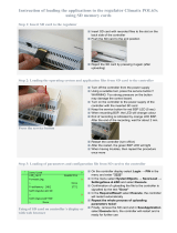
1.5. Assemble the HPS Daughter Card
The HPS daughter card (Optional) uses 40-pin HPS I/O on the DE10-Pro SX board to
provide peripheral interfaces such as UART, Gigabit Ethernet and USB OTG for HPS.
For how to assemble the HPS daughter card to the DE10-Pro SX board are shown in
below. Note: This card is optional, please contact Terasic’s sales department to
purchase the card.
Connect the HPS daughter card to the 40-pin I/O connector (see Figure 1-3)
of the DE10-Pro SX.

DE10-Pro
User Manual
12
www.terasic.com
September 30,
2020
Figure 1-3 Connect the HPS daughter card to the DE10-Pro SX
Lock the attachment screws to the HPS daughter card to secure it to the
DE10-Pro SX.
Figure 1-4 Lock the attachment screws to the HPS daughter card

DE10-Pro
User Manual
13
www.terasic.com
September 30,
2020
Set the DDR4A clock switch (SW7) to the “HPS”(ON) position for setting
DDR4A reference clock to 266.667Mhz for HPS application (See section 2.3
for detailed). The default setting of the SW7 is “FPGA”(OFF) position.
Figure 1-5 DDR4A reference clock switch
Figure 1-6 shows how the HPS daughter card is connected to the DE10-Pro SX
board.

DE10-Pro
User Manual
14
www.terasic.com
September 30,
2020
Figure 1-6 HPS daughter card connected with DE10-Pro SX
For a detailed interface on HPS daughter cards, see chapter 10 for more information.

DE10-Pro
User Manual
15
www.terasic.com
September 30,
2020
Chapter 2
Board Component
his chapter introduces all the important components on the DE10-Pro SX.
2.1 Board Overview
Figure 2-1 and Figure 2-2 is the top and bottom view of the DE10-Pro SX
development board. It depicts the layout of the board and indicates the location of the
connectors and key components. Users can refer to this figure for relative location of
the connectors and key components.
Figure 2-1 FPGA Board (Top)
T

DE10-Pro
User Manual
16
www.terasic.com
September 30,
2020
Figure 2-2 FPGA Board (Bottom)
2.2 Configuration Interface
This section describes the configuration mode for Stratix 10 SX FPGAs available on
the DE10-Pro SX. The peripheral circuits, switching modes, and usage scenarios for
each mode will be listed.
The DE10-Pro SX board supports the following configuration modes:
JTAG Mode (Configure the FPGA using the on-board USB-Blaster II).
Avalon® Streaming (Avalon® -ST) mode.
Active Serial (AS) mode
Users can use these modes to configure the FPGA or HPS (Hardware Process System)
fabric in the Stratix 10 SX FPGA and make the FPGA to run the user's logic or boot the
HPS to run the OS.
To switch between these modes, the user can change the MSEL[2:0] pin setting on the
FPGA via the MSEL switches (SW4 and SW5) on the DE10-Pro SX board (see Figure
2-3). Detailed MSEL[2:0] setting and corresponding configuration mode, please refer to
Table 2-2.

DE10-Pro
User Manual
17
www.terasic.com
September 30,
2020
Figure 2-3 The MSEL Switches
Table 2-2 The MSEL[2:0] Settings for Each Configuration mode
Configuration Mode
MSEL[2:0] Setting
Avalon-ST (x8)
110 (Factory Setting)
AS Fast
001
JTAG Only
111
We will introduce more detailed configuration mode in Table 2-2 in below.
Avalon-ST (x8) Mode
The Avalon® -ST configuration mode is a passive configuration scheme. This mode
configuration mode replaces the FPP mode available in earlier device families. It is the
fastest configuration mode for Stratix 10 devices. The DE10-Pro SX board supports x8
mode(8 bit data bus). This mode uses an external host (MAX 10 device on the
DE10-Pro SX board) to control the transfer of configuration data from an external
storage (CFI flash) to the FPGA.
Figure 2-4 shows the architecture of the Avalon-ST x8 mode on the DE10-Pro SX.

DE10-Pro
User Manual
18
www.terasic.com
September 30,
2020
Figure 2-4 Avalon-STx8 mode for DE10-Pro SX board
To use this mode, set MSEL[2:0] to "110" as shown in Figure 2-3.
In addition, for the configuration of the FPGA fabric, as shown in Figure 2-5, the CFI
flash on the DE10-Pro SX board defines two image address spaces, namely the
“factory” and “user” image space. The user can store two different designed in these
two locations, and through SW4 to switch which image will be booted (See Figure 2-6).
Figure 2-5 Two image space in the CFI flash

DE10-Pro
User Manual
19
www.terasic.com
September 30,
2020
Figure 2-6 Switch for select factory or user image
Active Serial (Fast) mode
In AS mode, the FPGA's configuration file is stored in the QSPI flash. The Secure
Device Manager (SDM) in Stratix 10 FPGA is responsible for the entire AS mode
process and interface. The SDM will load the initial configuration firmware from the
QSPI flash to configure the FPGA including FPGA I / O and core configuration. HPS
part of the boot can also be completed in this mode. Figure 2-7shows the architecture
of the AS mode of the DE10-Pro SX board.
Figure 2-7 AS mode for the DE10-Pro SX board
To use AS mode in DE10-Pro SX, please refer to Figure 2-8 and set MSEL[2:0] to
"001". For more information on the configuration of Stratix 10 FPGAs, please refer to
the file: Intel Stratix 10 Configuration User Guide

DE10-Pro
User Manual
20
www.terasic.com
September 30,
2020
Figure 2-8 AS mode setting for MSEL[2:0]
SoC FPGA boot
The boot process for Stratix 10 SoC FPGAs can be divided into two different methods:
FPGA Configuration First Mode
HPS Boot First Mode
The difference between the two methods is the initial difference between HPS and
FPGA fabric after powering on. More details can be found in the user documentation:
Intel Stratix 10 SoC FPGA Boot User Guide.
The factory setting of the SoC boot of the DE10-Pro SX board is the FPGA
Configuration First Mode. The architecture is shown in the Figure 2-9. Two storage
mediums are used. In this architecture, MSEL[2:0] needs to be set to AS mode.
The system needs QSPI flash on DE10-Pro SX as SDM flash for booting.
/