Page is loading ...


DE10-Standard
User Manual
1
www.terasic.com
March 20, 2018
CONTENTS
Chapter 1 DE10-Standard Development Kit ................................................. 4
1.1 Package Contents ....................................................................................................................... 4
1.2 DE10-Standard System CD........................................................................................................ 5
1.3 Getting Help ............................................................................................................................... 5
Chapter 2 Introduction of the DE10-Standard Board ..................................... 6
2.1 Layout and Components ............................................................................................................ 6
2.2 Block Diagram of the DE10-Standard Board ............................................................................ 8
Chapter 3 Using the DE10-Standard Board .................................................11
3.1 Settings of FPGA Configuration Mode .................................................................................... 11
3.2 Configuration of Cyclone V SoC FPGA on DE10-Standard ................................................... 12
3.3 Board Status Elements ............................................................................................................. 17
3.4 Board Reset Elements .............................................................................................................. 17
3.5 Clock Circuitry ......................................................................................................................... 19
3.6 Peripherals Connected to the FPGA ........................................................................................ 20
3.6.1 User Push-buttons, Switches and LEDs ................................................................ 20
3.6.2 7-segment Displays ............................................................................................... 23
3.6.3 2x20 GPIO Expansion Header .............................................................................. 25
3.6.4 HSMC Connector .................................................................................................. 27
3.6.5 24-bit Audio CODEC ............................................................................................ 30
3.6.6 I2C Multiplexer ..................................................................................................... 31
3.6.7 VGA Output .......................................................................................................... 32
3.6.8 TV Decoder ........................................................................................................... 35
3.6.9 IR Receiver ............................................................................................................ 37
3.6.10 IR Emitter LED ..................................................................................................... 37
3.6.11 SDRAM Memory .................................................................................................. 38

DE10-Standard
User Manual
2
www.terasic.com
March 20, 2018
3.6.12 PS/2 Serial Port ..................................................................................................... 40
3.6.13 A/D Converter and 2x5 Header ............................................................................. 41
3.7 Peripherals Connected to Hard Processor System (HPS) ........................................................ 42
3.7.1 User Push-buttons and LEDs ................................................................................ 42
3.7.2 Gigabit Ethernet .................................................................................................... 43
3.7.3 UART to USB ....................................................................................................... 44
3.7.4 DDR3 Memory ...................................................................................................... 45
3.7.5 Micro SD Card Socket .......................................................................................... 47
3.7.6 2-port USB Host .................................................................................................... 48
3.7.7 Accelerometer (G-sensor) ..................................................................................... 49
3.7.8 LTC Connector ...................................................................................................... 49
3.7.9 128x64 Dots LCD ................................................................................................. 50
Chapter 4 DE10-Standard System Builder ...................................................52
4.1 Introduction .............................................................................................................................. 52
4.2 Design Flow ............................................................................................................................. 53
4.3 Using DE10-Standard System Builder ..................................................................................... 54
Chapter 5 Examples For FPGA ...................................................................60
5.1 DE10-Standard Factory Configuration .................................................................................... 60
5.2 Audio Recording and Playing .................................................................................................. 61
5.3 Karaoke Machine ..................................................................................................................... 63
5.4 SDRAM Test in Nios II ............................................................................................................ 65
5.5 SDRAM Test in Verilog ........................................................................................................... 68
5.6 TV Box Demonstration ............................................................................................................ 69
5.7 TV Box Demonstration (VIP) .................................................................................................. 72
5.8 PS/2 Mouse Demonstration...................................................................................................... 74
5.9 IR Emitter LED and Receiver Demonstration ......................................................................... 77
5.10 ADC Reading ......................................................................................................................... 82
Chapter 6 Examples for HPS SoC ................................................................86
6.1 Hello Program .......................................................................................................................... 86

DE10-Standard
User Manual
3
www.terasic.com
March 20, 2018
6.2 Users LED and KEY ................................................................................................................ 88
6.3 I2C Interfaced G-sensor ........................................................................................................... 93
6.4 I2C MUX Test .......................................................................................................................... 96
6.5 SPI Interfaced Graphic LCD .................................................................................................... 98
6.6 Setup USB Wi-Fi Dongle ....................................................................................................... 101
6.7 Query Internet Time ............................................................................................................... 104
6.8 ALSA Audio Play ................................................................................................................... 105
Chapter 7 Examples for using both HPS SoC and FGPA ............................ 108
7.1 Required Background ............................................................................................................ 108
7.2 System Requirements ............................................................................................................. 109
7.3 AXI bridges in Intel SoC FPGA ............................................................................................. 109
7.4 GHRD Project ........................................................................................................................ 110
7.5 Compile and Programming .................................................................................................... 112
7.6 Develop the C Code ............................................................................................................... 113
Chapter 8 Programming the EPCS Device .................................................. 119
8.1 Before Programming Begins .................................................................................................. 119
8.2 Convert .SOF File to .JIC File ............................................................................................... 119
8.3 Write JIC File into the EPCS Device ..................................................................................... 124
8.4 Erase the EPCS Device .......................................................................................................... 125
Chapter 9 Linux BSP .................................................................................. 127
9.1 Use Linux BSP ....................................................................................................................... 127
9.2 Linux Console BSP ................................................................................................................ 128
9.3 Linux LXDE Desktop BSP .................................................................................................... 130
9.4 OpenCL BSP .......................................................................................................................... 131
Chapter 10 Appendix .................................................................................... 133
10.1 Revision History .................................................................................................................. 133
10.2 Copyright Statement ............................................................................................................ 133

DE10-Standard
User Manual
4
www.terasic.com
March 20, 2018
Chapter 1
DE10-Standard
Development Kit
The DE10-Standard Development Kit presents a robust hardware design platform built around the
Intel System-on-Chip (SoC) FPGA, which combines the latest dual-core Cortex-A9 embedded
cores with industry-leading programmable logic for ultimate design flexibility. Users can now
leverage the power of tremendous re-configurability paired with a high-performance, low-power
processor system. Intel’s SoC integrates an ARM-based hard processor system (HPS) consisting of
processor, peripherals and memory interfaces tied seamlessly with the FPGA fabric using a
high-bandwidth interconnect backbone. The DE10-Standard development board is equipped with
high-speed DDR3 memory, video and audio capabilities, Ethernet networking, and much more that
promise many exciting applications.
The DE10-Standard Development Kit contains all the tools needed to use the board in conjunction
with a computer that runs the Microsoft Windows XP or later.
1.1 Package Contents
Figure 1-1 The DE10-Standard package contents
The DE10-Standard package includes:

DE10-Standard
User Manual
5
www.terasic.com
March 20, 2018
• The DE10-Standard development board
• DE10-Standard Quick Start Guide
• USB cable (Type A to B) for FPGA programming and control
• USB cable (Type A to Mini-B) for UART control
• 12V DC power adapter
1.2 DE10-Standard System CD
The DE10-Standard System CD contains all the documents and supporting materials associated
with DE10-Standard, including the user manual, system builder, reference designs, and device
datasheets. Users can download this system CD from the link: http://de10-standard.terasic.com/cd/.
The developers can create their Quartus project based on the golden_top Quartus project included
in this CD. The golde_top Quartus project is placed in the folder: Demonstration/FPGA/golden_top.
Additionally, developers can use the System Builder software utility to create their Quartus project.
A detailed introduction of the software is given in Chapter 4
DE10-Standard System Builder.
1.3 Getting Help
Here are the addresses where you can get help if you encounter any problems:
• Terasic Technologies
• 9F., No.176, Sec.2, Gongdao 5th Rd, East Dist, Hsinchu City, 30070. Taiwan
Email: [email protected]
Tel.: +886-3-575-0880
Website: de10-standard.terasic.com

DE10-Standard
User Manual
6
www.terasic.com
March 20, 2018
Chapter 2
Introduction of the
DE10-Standard Board
This chapter provides an introduction to the features and design characteristics of the board.
2.1 Layout and Components
Figure 2-1 shows a photograph of the board. It depicts the layout of the board and indicates the
location of the connectors and key components.
Figure 2-1 DE10-Standard development board (top view)

DE10-Standard
User Manual
7
www.terasic.com
March 20, 2018
Figure 2-2 DE10-Standard development board (bottom view)
The DE10-Standard board has many features that allow users to implement a wide range of
designed circuits, from simple circuits to various multimedia projects.
The following hardware is provided on the board:
FPGA
• Intel Cyclone® V SE 5CSXFC6D6F31C6N device
• Serial configuration device – EPCS128
• USB-Blaster II onboard for programming; JTAG Mode
• 64MB SDRAM (16-bit data bus)
• 4 push-buttons
• 10 slide switches
• 10 red user LEDs
• Six 7-segment displays
• Four 50MHz clock sources from the clock generator
• 24-bit CD-quality audio CODEC with line-in, line-out, and microphone-in jacks
• VGA DAC (8-bit high-speed triple DACs) with VGA-out connector
• TV decoder (NTSC/PAL/SECAM) and TV-in connector
• PS/2 mouse/keyboard connector
• IR receiver and IR emitter
• One HSMC with Configurable I/O standard 1.5/1.8/2.5/3.3
• One 40-pin expansion header with diode protection
• A/D converter, 4-pin SPI interface with FPGA

DE10-Standard
User Manual
8
www.terasic.com
March 20, 2018
HPS (Hard Processor System)
• 925MHz Dual-core ARM Cortex-A9 MPCore processor
• 1GB DDR3 SDRAM (32-bit data bus)
• 1 Gigabit Ethernet PHY with RJ45 connector
• 2-port USB Host, normal Type-A USB connector
• Micro SD card socket
• Accelerometer (I2C interface + interrupt)
• UART to USB, USB Mini-B connector
• Warm reset button and cold reset button
• One user button and one user LED
• LTC 2x7 expansion header
• 128x64 dots LCD Module with Backlight
2.2 Block Diagram of the DE10-Standard Board
Figure 2-3 is the block diagram of the board. All the connections are established through the
Cyclone V SoC FPGA device to provide maximum flexibility for users. Users can configure the
FPGA to implement any system design.
Figure 2-3 Block diagram of DE10-Standard

DE10-Standard
User Manual
9
www.terasic.com
March 20, 2018
Detailed information about Figure 2-3 are listed below.
FPGA Device
• Cyclone V SoC 5CSXFC6D6F31C6N Device
• Dual-core ARM Cortex-A9 (HPS)
• 110K programmable logic elements
• 5,761 Kbits embedded memory
• 6 fractional PLLs
• 2 hard memory controllers
Configuration and Debug
• Quad serial configuration device – EPCS128 on FPGA
• Onboard USB-Blaster II (normal type B USB connector)
Memory Device
• 64MB (32Mx16) SDRAM on FPGA
• 1GB (2x256Mx16) DDR3 SDRAM on HPS
• Micro SD card socket on HPS
Communication
• Two port USB 2.0 Host (ULPI interface with USB type A connector)
• UART to USB (USB Mini-B connector)
• 10/100/1000 Ethernet
• PS/2 mouse/keyboard
• IR emitter/receiver
• I2C multiplexer
Connectors
• One HSMC (Configurable I/O standards 1.5/1.8/2.5/3.3V)
• One 40-pin expansion headers
• One 10-pin ADC input header
• One LTC connector (one Serial Peripheral Interface (SPI) Master, one I2C and one GPIO
interface)
Display
• 24-bit VGA DAC
• 128x64 dots LCD Module with Backlight
Audio
• 24-bit CODEC, Line-in, Line-out, and microphone-in jacks
Video Input

DE10-Standard
User Manual
10
www.terasic.com
March 20, 2018
• TV decoder (NTSC/PAL/SECAM) and TV-in connector
ADC
• Interface: SPI
• Fast throughput rate: 500 KSPS
• Channel number: 8
• Resolution: 12-bit
• Analog input range : 0 ~ 4.096
Switches, Buttons, and Indicators
• 5 user Keys (FPGA x4, HPS x1)
• 10 user switches (FPGA x10)
• 11 user LEDs (FPGA x10, HPS x 1)
• 2 HPS reset buttons (HPS_RESET_n and HPS_WARM_RST_n)
• Six 7-segment displays
Sensors
• G-Sensor on HPS
Power
• 12V DC input

DE10-Standard
User Manual
11
www.terasic.com
March 20, 2018
Chapter 3
Using the
DE10-Standard Board
This chapter provides an instruction to use the board and describes the peripherals.
3.1 Settings of FPGA Configuration Mode
When the DE10-Standard board is powered on, the FPGA can be configured from EPCS or HPS.
The MSEL[4:0] pins are used to select the configuration scheme. It is implemented as a 6-pin DIP
switch SW10 on the DE10-Standard board, as shown in Figure 3-1.
Figure 3-1 DIP switch (SW10) setting of Active Serial (AS) mode on DE10-Standard board
Table 3-1 shows the relation between MSEL[4:0] and DIP switch (SW10).
Table 3-1 FPGA Configuration Mode Switch (SW10)
Board Reference
Signal Name
Description
Default
AS Mode
SW10.1
MSEL0
Use these pins to set the FPGA
Configuration scheme
OFF (“1”)
SW10.2
MSEL1
ON (“0”)

DE10-Standard
User Manual
12
www.terasic.com
March 20, 2018
SW10.3
MSEL2
ON (“0”)
SW10.4
MSEL3
OFF (“1”)
SW10.5
MSEL4
ON (“0”)
SW10.6
N/A
N/A
N/A
Figure 3-1 shows MSEL[4:0] setting of AS mode, which is also the default setting on
DE10-Standard. When the board is powered on, the FPGA is configured from EPCS, which is
pre-programmed with the default code. If developers wish to reconfigure FPGA from an application
software running on Linux, the MSEL[4:0] needs to be set to “01010” before the programming
process begins.
Table 3-2 MSEL Pin Settings for FPGA Configure of DE10-Standard
MSEL[4:0]
Configure Scheme
Description
10010
AS
FPGA configured from EPCS (default)
01010
FPPx32
FPGA configured from HPS software: Linux
3.2 Configuration of Cyclone V SoC FPGA on DE10-Standard
There are two types of programming method supported by DE10-Standard:
1. JTAG programming: It is named after the IEEE standards Joint Test Action Group.
The configuration bitstream is downloaded directly into the Cyclone V SoC FPGA. The FPGA will
retain its current status as long as the power keeps applying to the board; the configuration
information will be lost when the power is off.
2. AS programming: The other programming method is Active Serial configuration.
The configuration bitstream is downloaded into the quad serial configuration device (EPCS128),
which provides non-volatile storage for the bit stream. The information is retained within EPCS128
even if the DE10-Standard board is turned off. When the board is powered on, the configuration
data in the EPCS128 device is automatically loaded into the Cyclone V SoC FPGA.
JTAG Chain on DE10-Standard Board
The FPGA device can be configured through JTAG interface on DE10-Standard board, but the
JTAG chain must form a closed loop, which allows Quartus II programmer to the detect FPGA
device. Figure 3-2 illustrates the JTAG chain on DE10-Standard board.

DE10-Standard
User Manual
13
www.terasic.com
March 20, 2018
Figure 3-2 Path of the JTAG chain
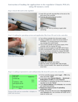
Configure the FPGA in JTAG Mode
There are two devices (FPGA and HPS) on the JTAG chain. The following shows how the FPGA is
programmed in JTAG mode step by step.
1. Open the Quartus II programmer and click “Auto Detect”, as circled in Figure 3-3
Figure 3-3 Detect FPGA device in JTAG mode
2. Select detected device associated with the board, as circled in Figure 3-4.

DE10-Standard
User Manual
14
www.terasic.com
March 20, 2018
Figure 3-4 Select 5CSXFC6D6 device
3. Both FPGA and HPS are detected, as shown in Figure 3-5.
Figure 3-5 FPGA and HPS detected in Quartus programmer
4. Right click on the FPGA device and open the .sof file to be programmed, as highlighted in
Figure 3-6.

DE10-Standard
User Manual
15
www.terasic.com
March 20, 2018
Figure 3-6 Open the .sof file to be programmed into the FPGA device
5. Select the .sof file to be programmed, as shown in Figure 3-7.
Figure 3-7 Select the .sof file to be programmed into the FPGA device
6. Click “Program/Configure” checkbox and then click “Start” button to download the .sof file

DE10-Standard
User Manual
16
www.terasic.com
March 20, 2018
into the FPGA device, as shown in Figure 3-8.
Figure 3-8 Program .sof file into the FPGA device
Configure the FPGA in AS Mode
• The DE10-Standard board uses a quad serial configuration device (EPCS128) to store
configuration data for the Cyclone V SoC FPGA. This configuration data is automatically
loaded from the quad serial configuration device chip into the FPGA when the board is
powered up.
• Users need to use Serial Flash Loader (SFL) to program the quad serial configuration
device via JTAG interface. The FPGA-based SFL is a soft intellectual property (IP) core within
the FPGA that bridge the JTAG and Flash interfaces. The SFL Megafunction is available in
Quartus II. Figure 3-9 shows the programming method when adopting SFL solution.
• Please refer to Chapter 9: Steps of Programming the Quad Serial Configuration Device for
the basic programming instruction on the serial configuration device.

DE10-Standard
User Manual
17
www.terasic.com
March 20, 2018
Figure 3-9 Programming a quad serial configuration device with SFL solution
3.3 Board Status Elements
In addition to the 10 LEDs that FPGA device can control, there are 5 indicators which can indicate
the board status (See Figure 3-10), please refer the details in Table 3-3.
Figure 3-10 LED Indicators on DE10-Standard
Table 3-3 LED Indicators
Board Reference
LED Name
Description
D14
12-V Power
Illuminates when 12V power is active.
TXD
UART TXD
Illuminates when data is transferred from FT232R to USB Host.
RXD
UART RXD
Illuminates when data is transferred from USB Host to FT232R.
D5
JTAG_RX
Reserved
D4
JTAG_TX
3.4 Board Reset Elements
There are two HPS reset buttons on DE10-Standard, HPS (cold) reset and HPS warm reset, as
shown in Figure 3-11. Table 3-4 describes the purpose of these two HPS reset buttons. Figure 3-12
is the reset tree for DE10-Standard.

DE10-Standard
User Manual
18
www.terasic.com
March 20, 2018
Figure 3-11 HPS cold reset and warm reset buttons on DE10-Standard
Table 3-4 Description of Two HPS Reset Buttons on DE10-Standard
Board Reference
Signal Name
Description
KEY5
HPS_RESET_N
Cold reset to the HPS, Ethernet PHY and USB host device.
Active low input which resets all HPS logics that can be reset.
KEY7
HPS_WARM_RST_N
Warm reset to the HPS block. Active low input affects the
system reset domain for debug purpose.

DE10-Standard
User Manual
19
www.terasic.com
March 20, 2018
Figure 3-12 HPS reset tree on DE10-Standard board
3.5 Clock Circuitry
Figure 3-13 shows the default frequency of all external clocks to the Cyclone V SoC FPGA. A
clock generator is used to distribute clock signals with low jitter. The four 50MHz clock signals
connected to the FPGA are used as clock sources for user logic. One 25MHz clock signal is
connected to two HPS clock inputs, and the other one is connected to the clock input of Gigabit
Ethernet Transceiver. Two 24MHz clock signals are connected to the clock inputs of USB
Host/OTG PHY and USB hub controller. The associated pin assignment for clock inputs to FPGA
I/O pins is listed in Table 3-5.
/