Page is loading ...


HAN Pilot Platform
Demonstration Manual
1
www.terasic.com
October 8, 2019
TABLE OF CONTENTS
Chapter 1 Introduction ............................................................................................. 3
Chapter 2 Examples for FPGA ................................................................................. 4
2.1 Factory Default Code ................................................................................................................................. 4
2.2 Nios II Control for Programmable PLL/ Temperature/ Power/ 9-axis ....................................................... 6
2.3 Nios DDR4 SDRAM Test ........................................................................................................................ 12
2.4 RTL DDR4 SDRAM Test ......................................................................................................................... 14
2.5 USB Type-C DisplayPort Alternate Mode ............................................................................................... 15
2.6 USB Type-C FX3 Loopback .................................................................................................................... 17
2.7 HDMI TX and RX in 4K Resolution ........................................................................................................ 21
2.8 HDMI TX in 4K Resolution ..................................................................................................................... 26
2.9 Low Latency Ethernet 10G MAC Demo .................................................................................................. 29
2.10 Socket Server .......................................................................................................................................... 33
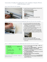
2.11 Auto Fan Speed Control .......................................................................................................................... 40
Chapter 3 Examples for HPS SoC .......................................................................... 44
3.1 User LED and KEY .................................................................................................................................. 44
3.2 Setup USB Wi-Fi Dongle ......................................................................................................................... 48
3.3 HPS GPIO Header .................................................................................................................................... 51
3.4 Network Socket ........................................................................................................................................ 55
Chapter 4 Examples for Using both HPS SoC and FPGA ....................................... 61
4.1 Required Background ............................................................................................................................... 61
4.2 System Requirements ............................................................................................................................... 61
4.3 AXI bridges in Intel SoC FPGA ............................................................................................................... 62
4.4 GHRD Project .......................................................................................................................................... 63
4.5 Compile and Programming ....................................................................................................................... 64
4.6 Develop the C Code .................................................................................................................................. 64
Chapter 5 PCI Express Design for Windows ........................................................... 69

HAN Pilot Platform
Demonstration Manual
2
www.terasic.com
October 8, 2019
5.1 PCI Express System Infrastructure ........................................................................................................... 69
5.2 PC PCI Express Software SDK ................................................................................................................ 70
5.3 PCI Express Software Stack ..................................................................................................................... 70
5.4 PCI Express Library API .......................................................................................................................... 75
5.5 PCIe Reference Design – Fundamental .................................................................................................... 79
5.6 PCIe Reference Design - DDR4 ............................................................................................................... 85
Chapter 6 PCI Express Design for Linux ................................................................ 92
6.1 PCI Express System Infrastructure ........................................................................................................... 92
6.2 PC PCI Express Software SDK ................................................................................................................ 93
6.3 PCI Express Software Stack ..................................................................................................................... 93
6.4 PCI Express Library API .......................................................................................................................... 96
6.5 PCIe Reference Design – Fundamental .................................................................................................. 100
6.6 PCIe Reference Design - DDR4 ............................................................................................................. 105
Chapter 7 Linux BSP ........................................................................................... 112
7.1 Introduction ............................................................................................................................................ 112
7.2 Use Linux BSP ....................................................................................................................................... 112
7.3 Linux LXDE VNC Desktop BSP ........................................................................................................... 113
7.4 Linux LXDE HDMI Desktop BSP ......................................................................................................... 113
7.5 VNC Desktop OpenCL BSP ................................................................................................................... 114

HAN Pilot Platform
Demonstration Manual
3
www.terasic.com
October 8, 2019
Chapter 1
Introduction
This manual will introduce the various application demonstrations on HAN Pilot Platform. These
demonstrations cover most of the interfaces on HAN Pilot Platform. Let users familiarize using
these interfaces of the HAN Pilot Platform. Demonstration according to FPGA and HPS Fabrics are
divided into three categories:
Pure use of FPGA fabric resources (Chapter 2)
Pure use of HPS fabric resources (Chapter 3)
Use both FPGA and HPS fabric resources (Chapter 4)
In addition, the PCIe example of HAN Pilot Platform will be described separately in one chapter
(Chapter 5) because of its high content.
Finally, to complete the following demonstration, user needs to install the following software in the
computer:
Intel Quartus® Prime Design Software Version 18.1 or later.
Intel SoC Embedded Design Suite (EDS)

HAN Pilot Platform
Demonstration Manual
4
www.terasic.com
October 8, 2019
Chapter 2
Examples for FPGA
This chapter provides examples of advance designs implemented by RTL or Qsys on the HAN Pilot
Platform. These reference designs cover the features of peripherals connected to the FPGA, such as
DDR4, PCIe, HDMI and USB Controller. All the associated files can be found in the directory
\Demonstrations\FPGA of HAN Pilot Platform system CD.
2
2.
.1
1
F
Fa
ac
ct
to
or
ry
y
D
De
ef
fa
au
ul
lt
t
C
Co
od
de
e
The HAN Pilot Platform has a default configuration bit-stream pre-programmed, which
demonstrates some of the basic features on board. This demo used LED,7-Segments, Switch, HDMI
transmitter display and fan control.
Function Block Diagram
Figure 2-1 shows the function block diagram of this demonstration. This demo used fan controller
to control fan and used frame buffer read board picture from ON-CHIP-MEMORY and used scaler
scale the picture to 1920x1080 size, display the picture by HDMI TX.
Figure 2-1 Block Diagram of Default Demonstration

HAN Pilot Platform
Demonstration Manual
5
www.terasic.com
October 8, 2019
Design Tools
Quartus Prime 18.1.0 Standard Edition
Demonstration Source Code:
Project Directory: Demonstration\default_code
Bit Stream: default_code.sof or default_code.jic
Demonstration Batch File: default_code\demo_batch or default_code\demo_run_batch
NOTE: because the demo included software, and run on on-chip-memory, so use mem_init can
package elf to sof, so user can only program .sof or .sof and .elf to run demo.
The demo batch file includes following files:
Batch File: test.bat
FPGA Configuration File: default_code.sof or default_code.jic
Demonstration Setup
1. Make sure Quartus Prime is installed on the host PC.
2. Connect HAN Pilot Platform to the host PC via USB cable. Install the USB-Blaster II driver if
necessary.
3. Connect the HDMI TX to displayer via HDMI cable.
4. Set MSEL[2:0] to 010, set SW0 to 0, SW1 to 0.
5. Power on the HAN Pilot Platform.
6. Execute the demo batch file “test.bat” under the batch file folder \ default_code\demo_batch.
You will see the menu as shown in Figure 2-2.
7. Select your choice, and program FPGA or program flash.
8. When the demo is running, you can see the LED is blinking and flowing, and the displayer will
display the board picture as shown in Figure 2-3.
Figure 2-2 Menu of Default Demonstration

HAN Pilot Platform
Demonstration Manual
6
www.terasic.com
October 8, 2019
Figure 2-3 Board Picture of Default Demonstration
2
2.
.2
2
N
Ni
io
os
s
I
II
I
C
Co
on
nt
tr
ro
ol
l
f
fo
or
r
P
Pr
ro
og
gr
ra
am
mm
ma
ab
bl
le
e
P
PL
LL
L/
/
T
Te
em
mp
pe
er
ra
at
tu
ur
re
e/
/
P
Po
ow
we
er
r/
/
9
9-
-a
ax
xi
is
s
This demonstration shows how to use the Nios II processor to program two programmable
oscillators (CDCM6208 and TXC) on the FPGA board, how to measure the power consumption
based on the built-in power measure circuit. The demonstration also includes a function of
monitoring system temperature with the on-board temperature sensor, and 3-axis gyroscope, 3-axis
accelerometer, and 3-axis magnetometer output with the on-board MPU-9250 Motion Tracking
device.
System Block Diagram
Figure 2-4 shows the system block diagram of this demonstration. The system requires a 50 MHz
clock provided from the board. The five peripherals (including temperature sensor, power monitor,
CDCM6208, TXC, and MPU-9250) are all controlled by Nios II through the PIO controller, and all
of them are programmed through I2C protocol which is implemented in the C code. The I2C pins
from chip are connected to Qsys System Interconnect Fabric through PIO controllers. The Nios II
program toggles the PIO controller to implement the I2C protocol. The Nios II program is running
in the on-chip memory.

HAN Pilot Platform
Demonstration Manual
7
www.terasic.com
October 8, 2019
Figure 2-4 Block Diagram of the Nios II Basic Demonstration
The program provides a menu in nios-terminal, as shown in Figure 2-5 to provide an interactive
interface. With the menu, users can perform the test for the temperature sensor, power monitor,
external programmable PLL and 9-axis outputs. Note, pressing ‘ENTER’ should be followed with
the choice number.
Figure 2-5 Menu of Demo Program

HAN Pilot Platform
Demonstration Manual
8
www.terasic.com
October 8, 2019
In temperature test, the program will display local temperature and remote temperature. The remote
temperature is the FPGA temperature, and the local temperature is the board temperature where the
temperature sensor located.
A power monitor IC (LTC2945) embedded on the board can monitor Arria10 real-time current and
power. This IC can work out current/power value as multiplier and divider are embedded in it.
There is a sense resistor R176 (0.006 Ω) for LTC2945 in the circuit, when power on the HAN Pilot
Platform, there will be a voltage drop (named ∆SENSE Voltage) on R176. Based on sense resistors,
the program of power monitor can calculate the associated voltage, current and power consumption
from the LTC2945 through the I2C interface. Please note the device I2C address is 0xD4.
The MPU-9250 consists of two dies, one die houses the 3-axis gyroscope and 3-axis accelerometer,
and the other die houses the a-axis magnetometer. Similarly, the MPU-9250 provides complete
9-axis output through the I2C interface.
In the external PLL programming test, the program will program the PLL first, and subsequently
will use TERASIC QSYS custom CLOCK_COUNTER IP to count the clock count in a specified
period to check whether the output frequency is changed as configured. For CDCM6208
programming, the program can control the CDCM6208 to configure the output frequency of
SATA/PCIE/DDR4A/DDR4B/DDR4H REFCLK according to your choice. Please note the device
I2C address is 0xA8. For TXC programming, the program can control the TXC to configure the
output frequency of HDMI/SFP+/FMC/DP/USB REFCLK according to your choice. There are five
TXC’s ICs for clock generator, divided into two group, TXCA and TXCB. The HDMI and SFP+
reference clock generators share the same I2C bus, REFCLK0_SCL/REFCLK0_SDA, and are
grouped into TXCA. The FMC, DP, and USB reference clock generators also share the same I2C
bus, REFCLK1_SCL/REFCLK1_SDA, and are grouped into TXCB.
Demonstration File Location
Hardware project directory: Basic_Demo
Bitstream used: Basic_Demo.sof
Software project directory: Basic_Demo \software
Demo batch file: Basic_Demo\demo_batch\test.bat, test.sh
Demonstration Setup and Instructions
1. Make sure Quartus Prime is installed on the host PC.
2. Set MSEL[2:0] to 010
3. Power on the FPGA board.
4. Use the USB Cable to connect your PC and the FPGA board and install USB Blaster II driver if
necessary.
5. Execute the demo batch file “test.bat” under the batch file folder: Basic_Demo\demo_batch.
6. After the Nios II program is downloaded and executed successfully, a prompt message will be
displayed in nios2-terminal.

HAN Pilot Platform
Demonstration Manual
9
www.terasic.com
October 8, 2019
7. For temperature test, please input key ‘0’ and press ‘Enter’ in the nios-terminal, as shown in
Figure 2-6.
Figure 2-6 Temperature Demo
8. For power monitor test, please input key ‘1’ and press ‘Enter’ in the nios-terminal, the Nios II
console will display the values of voltage, current and power as shown in Figure 2-7.
Figure 2-7 Power Monitor Demo
9. For 9-axis test, please input key ‘2’ and press ‘Enter’ in the nios-terminal, the Nios II console
will display the values of 9-axis as shown in Figure 2-8.

HAN Pilot Platform
Demonstration Manual
10
www.terasic.com
October 8, 2019
Figure 2-8 MPU-9250 Demo
10. For programmable PLL TXCA test, please input key ‘3’ and press ‘Enter’ in the nios-terminal
first, then select the desired output frequency of HDMI/SFP+ REFCLK, as shown in Figure
2-9.
Figure 2-9 TXCA Demo
11. For programmable PLL TXCB test, please input key ‘4’ and press ‘Enter’ in the nios-terminal
first, then select the desired output frequency of DP/USB/FMC REFCLK, as shown in Figure
2-10.

HAN Pilot Platform
Demonstration Manual
11
www.terasic.com
October 8, 2019
Figure 2-10 TXCB Demo
12. For programmable PLL CDCM6208 test, please input key ‘5’ and press ‘Enter’ in the
nios-terminal first, then select the desired output frequency of SATA/ PCIE/ DDR4A/ DDR4B/
DDR4H REFCLK, as shown in Figure 2-11.
Figure 2-11 CDCM6208 Demo

HAN Pilot Platform
Demonstration Manual
12
www.terasic.com
October 8, 2019
2.3 Nios DDR4 SDRAM Test
Many applications use a high performance RAM, such as a DDR4 SDRAM, to provide temporary
storage. In this demonstration hardware and software designs are provided to illustrate how to
perform DDR4 memory access in QSYS. We describe how the Altera’s “Arria 10 External Memory
Interfaces” IP is used to access the two DDR4-Sodimm on the FPGA board, and how the Nios II
processor is used to read and write the SDRAM for hardware verification. The DDR4 SDRAM
controller handles the complex aspects of using DDR4 SDRAM by initializing the memory devices,
managing SDRAM banks, and keeping the devices refreshed at appropriate intervals.
System Block Diagram
Figure 2-12 shows the system block diagram of this demonstration. The QSYS system requires one
50 MHz and two 266.667MHz clock source. The two 266.667 MHz clock source is provided by
CDCM6208 clock generator on the board. The 50MHz is used by IO PLL to generate 200MHz for
Nios Processor and On-chip Memory. The two 266.667MHz clock are used as reference clocks for
the DDR4 controllers. There are two DDR4 Controllers are used in the demonstrations. Each
controller is responsible for one DDR4 SDRAM. Each DDR4 controller is configured as a 1 GB
DDR4-1066MHz controller. The DDR4A controllers are designed as 1GB rather 4GB is due to
address space limitation of Nios II processor. Nios II processor is used to perform memory test. The
Nios II program is running in the On-Chip Memory. A PIO Controller is used to monitor buttons
status which is used to trigger starting memory testing.
Figure 2-12 Block Diagram of the DDR4 Basic Demonstration
The system flow is controlled by a Nios II program. First, the Nios II program writes test patterns
into the whole 1 GB of SDRAM. Then, it calls Nios II system function (alt_dache_flush_all) to
make sure all data has been written to SDRAM. Finally, it reads data from SDRAM for data

HAN Pilot Platform
Demonstration Manual
13
www.terasic.com
October 8, 2019
verification. The program will show progress in JTAG-Terminal when writing/reading data to/from
the SDRAM. When verification process is completed, the result is displayed in the JTAG-Terminal.
Design Tools
Quartus Prime 18.1.0 Standard Edition
Nios II Software Build Tools for Eclipse 18.1
Demonstration Source Code
Quartus Project directory: NIOS_DDR4
Nios II Eclipse: NIOS_DDR4 \software
Nios II Project Compilation
Nios II Project Compilation
Before you attempt to compile the reference design under Nios II Eclipse, make sure the project is
cleaned first by clicking ‘Clean’ from the ‘Project’ menu of Nios II Eclipse.
Demonstration Batch File
Demo Batch File Folder: NIOS_DDR4 \demo_batch
The demo batch file includes following files:
Batch File for USB-Blaster II: test.bat, test.sh
FPGA Configure File: NIOS_DDR4.sof
Nios II Program: DDR4_Test.elf
Demonstration Setup
Please follow below procedures to setup the demonstration.
1. Make sure Quartus Prime and Nios II are installed on your PC.
2. Make sure DDR4 SODIMM are installed on the FPGA board.
3. Set MSEL[2:0] to 010。
4. Power on the FPGA board.
5. Use USB Cable to connect PC and the FPGA board and install USB Blaster II driver if
necessary.
6. Execute the demo batch file “test.bat” under the folder “NIOS_DDR4\demo_batch”.
7. After Nios II program is downloaded and executed successfully, a prompt message will be
displayed in nios2-terminal.
8. Press Key0~Key1 of the FPGA board to start SDRAM verify process. Press Key0 for continued
test.
9. The program will display progressing and result information, as shown in Figure 2-13.

HAN Pilot Platform
Demonstration Manual
14
www.terasic.com
October 8, 2019
Figure 2-13 Progress and Result Information for the DDR4 Demonstration
2.4 RTL DDR4 SDRAM Test
This demonstration performs a memory test function on the one DDR4 SO-DIMM (DDR4A) and
one DDR4 Component (DDR4B) on the HAN Pilot Platform. The memory size of DDR4
SO-DIMM is 4GB and DDR4 Component is 1GB.
Function Block Diagram
Figure 2-14 shows the function block diagram of this demonstration. There are two DDR4 SDRAM
controllers. The controller uses 266.667 MHz as a reference clock. It generates one 1066MHz clock
as memory clock from the FPGA to the memory and the controller itself runs at quarter-rate in the
FPGA i.e. 266.667 MHz.
Figure 2-14 Block Diagram of DDR4 x2 Demonstration
Design Tools
Quartus Prime 18.1.0 Standard Edition
Demonstration Source Code:

HAN Pilot Platform
Demonstration Manual
15
www.terasic.com
October 8, 2019
Project Directory: Demonstration\RTL_DDR4
Bit Stream: RTL_DDR4.sof
Demonstration Batch File
Demo Batch File Folder: RTL_DDR4 \demo_batch
The demo batch file includes following files:
Batch File: test.bat
FPGA Configuration File: RTL_DDR4.sof
Demonstration Setup
1. Make sure Quartus Prime is installed on the host PC.
2. Connect HAN Pilot Platform to the host PC via USB cable. Install the USB-Blaster II driver if
necessary.
3. Set MSEL[2:0] to 010。
4. Power on the HAN Pilot Platform.
5. Execute the demo batch file “test.bat” under the batch file folder \ RTL_DDR4\demo_batch.
6. Press KEY0 on HAN Pilot Platform to start the verification process. When KEY0 is released,
LED0, LED1 should start blinking. After approximately 2 seconds, LED1 and LED2 should
stop blinking and stay on to indicate the DDR4 (A) and DDR4 (B) have passed the test,
respectively. Table 2-1 lists the LED indicators.
7. If LED0 or LED1 does not start blinking upon releasing KEY0, it indicates local_cal_success of
the corresponding DDR4 fails.
8. If LED0 or LED1 fail to remain on after 2 seconds, the corresponding DDR4 test has failed.
9. Press KEY0 again to regenerate the test control signals for a repeat test.
Table 2-1 LED Indicators
Name
Description
LED0
DDR4 (A) test result
LED1
DDR4 (B) test result
2.5 USB Type-C DisplayPort Alternate Mode
This section introduces how to implement a DisplayPort Source based on USB Type-C DisplayPort
Alternate Mode. The demo includes two major parts: DisplayPort and USB Type-C.
For DisplayPort design, DisplayPort Intel FPGA IP is used to generate DisplayPort TX video. The
DisplayPort design is refer to the document :Arria 10 DisplayPort Design Example using on board
connector (TX Only).
For USB Type-C, system need to monitor the information sent from the USB Type-C Port
Controller CYPD3125 (EZ-PD CCG3). From the sent information, system can know whether the
plug-in device is a DisplayPort monitor and the DP lane number is 4 or 2, and system have to
configure the DisplayPort crossbar switch so the FPGA transceiver signals can be routed to the

HAN Pilot Platform
Demonstration Manual
16
www.terasic.com
October 8, 2019
type-c port correctly.
The Quartus Project USBC_DP_4K is designed for 4K monitor, and USBC_DP_FullHD is design
for Full HD Monitor. If your Type-C monitor only supports Full HD, please use the
USB_DP_FullHD for the demo setup.
System Block Diagram
Figure 2-15 shows the system block diagram for the DisplayPort Demo. When a Type-C monitor is
plugged into the Type-C Connector, the Type-C Port Controller (EZ-PD CCG3) will enable 5V
power for the monitor. When a Type-C device is plug-in or removed from the Type-C connector, the
CCG3 will notify FPGA through the IC2 interface. CCG3 will sends one byte data to 0 offset
address in the I2C Slave Port. The meaning of the data is shown in Table 2-2. If attached device is a
DisplayPort monitor, then DisplayPort crossbar switch is configured so the transceivers signals are
routed to the type-c connector correctly.
For DisplayPort design, the Hot Plug Detect (HPD) causes the DisplayPort source to initialize the
link via AUX channel. The DisplayPort IP generates parallel Video data and FPGA transceivers are
used to serial the video data. For 4K video data, 4 TX transceivers are used with reference clock
270 MHz. For Full HD video data, 4 or 2 TX transceivers are used. The input video data for
DisplayPort IP is generated by VIP Test Pattern Generator II IP and VIP Clocked Video Output II IP.
In the system, a Nios II processor is used to control the DisplayPort IP. The Nios II Processor is
running on on-chip memory with 100Mhz.
Figure 2-15 Block Diagram of DisplayPort Demo
Table 2-2 Information sent by CCG3
Data[6:5]
Description
0
No Device is attached
1
Only USB 3.1 Device is attached
2
4 Lane DisplayPort monitor is attached
3
USB and 2 Lane DisplayPort monitor is attached

HAN Pilot Platform
Demonstration Manual
17
www.terasic.com
October 8, 2019
Data[4]
Description
0
Cable is normal
1
Cable is flip
Demonstration File Locations
For 4K Video Output:
Hardware project directory: USBC_DP_4K
Bitstream used: USBC_DP_golden_top.sof
Nios II Program: dp_demo_test.elf
Demo batch file: USBC_DP_4K\demo_batch\test.bat
For Full-HD Video Output:
Hardware project directory: USBC_DP_FullHD
Bitstream used: USBC_DP.sof.sof
Nios II Program: dp_demo_test.elf
Demo batch file: USBC_DP_FullHD\demo_batch\test.bat
Demonstration Setup and Instructions
1. Make sure Quartus Prime is installed on your PC.
2. Set MSEL[2:0] to 010。
3. Power on the FPGA board.
4. Use the Mini USB Cable to connect your PC and the FPGA board and install USB Blaster II
driver if necessary.
5. Execute test.bat under the demo_batch folder.
6. Connect USB Type-C Connector (J2) to a 4K Type-C Monitor (or Full HD Type-C Monitor) via
a Type-C Cable.
7. You will see a color bar pattern on the Type-C Monitor.
2.6 USB Type-C FX3 Loopback
This demonstration illustrates how the FX3 is working with the FPGA for USB3.0/USB2.0 data
bulk in/out (data loop transmission). There is a USB type-C connector onto HAN Pilot Platform, a
type-C cable is reversible for plugging in the USB type-C connector. This demonstration also
implements the auto-switching mechanism for a type-C cable plugging in on either side.
Function Block Diagram
Figure 2-16 shows the function block diagram of the USBC_FX3 demonstration. This design
comprises two parts, USB3.0/USB2.0 TX&RX crossbar switch controlling and FX3 data
transferring. As the Type-C connector is reversible, a Type-C port Controller (CYPD3125) is
required for USB3.0/USB2.0 TX&RX crossbar switch controlling. When the Type-C cable is

HAN Pilot Platform
Demonstration Manual
18
www.terasic.com
October 8, 2019
plugged in, the CC (Configuration Channel) signal is communicating with the controller. The
controller then transfers the data to the Slave IC (FPGA) by I2C in Master mode, and There will be
a salve I2C module in the FPGA to decode the signal and send the control signal to control the
RX/TX direction of the PI3USB31532 USB3.0 signal. Here is a LED0 on the board to indicate the
cable plugging direction, and LED1 indicates whether there is a USB connection signal or not. For
the data transmission of FX3 module, FIFO and controller (implemented in the FPGA) combine
FX3 module to perform the data bulk in/out loop. (For details, please refer to CYPRESS AN65974
Designing with the EZ-USB® FX3™ Slave FIFO Interface Chapter 11). All modules functions are
described below:
USB_AUTO_DETECT: This module can decode the I2C signal from the Type-C Port Controller
(CYPD3125 IC), then timely switch the RX/TX direction of Type-C port (by controlling the
PI3USB31532 IC) and control the USB 3.0 Mux/Demux9 (HD3SS3212) switching to transfer the
USB 3.0 signal to FX3 module. As shown in Figure 4-1, the LED0 indicates the Type-C connector
RX/TX direction, the LED1 indicates the USB 3.0 signal input.
LOOPBACK: This module is designed as FX3 Slave FIFO Interface, the module combines the
CYPRESS application(bulkloop.exe) to implement data bulk in/out loop demo.
KEY0: It is used to reset FX3 module.
PMODE[2:0]: The HAN Pilot Platform has a 4Mbits Flash ROM, which can be used to program
the FX3 firmware. This ROM is connected to FX3 through SPI interface. PMODE[2:0] is used to
set the FX3 in program or boot status. The setting details is described in below steps.
Figure 2-16 Block diagram of the USBC FX3 design
Demonstration Setup
Hardware Setting Up, as shown in Figure 2-17.

HAN Pilot Platform
Demonstration Manual
19
www.terasic.com
October 8, 2019
Figure 2-17 USBC FX3 Demo Hardware Setting Up
Design Tools
Quartus Prime 18.1 Standard Edition
Demonstration Source Code
Quartus project directory: USBC_FX3
Bitstream used: USBC_FX3.sof
Demonstration Batch File
Demo batch file folder: demonstrations\USBC_FX3\demo_batch
Demonstration Setup
Connect the HAN Pilot Platform USB Blaster II connector (J20) to the host PC with a USB
cable and install the USB-Blaster II driver if necessary.
Use a Type-C cable to connect the HAN Pilot Platform and a PC (with a Type-C connector).
As shown in Figure 2-17.
Plug the 12V adapter to HAN Pilot Platform DC 12V power connector (J28).
Set MSEL[2:0] to 010.
Power on the HAN Pilot Platform.
Execute the demo batch file “test.bat” from the directory \FPGA\USBC_FX3\demo_batch.
Install the FX3 driver: the driver for Windows 7 is in the \ FPGA\ USBC_FX3\
demo_batch\ Driver\ win7 folder, and the driver for Windows 10 is in the \ FPGA\
USBC_FX3\ demo_batch\ Driver\ win10 folder.
Use JP6, JP5, JP4 to set the PMODE[2:0] as “0F1” (F indicates floating).
Press KEY0 (RESET FX3).
Re-plug the Type-C cable one time, Cypress Control Center will show Cypress FX3 USB
Streamer Example Device and BOS (SuperSpeed Device capability), it indicates the
USB3.0 Has completed the setup. When LED1 lights up, it indicates USB signal is
detected. LED0 lights off indicates Type-C Cable two sides plugged with same directions,
/