Page is loading ...

Apollo-S10
User Manual
1
www.terasic.com
October 14,
2020
1.1. W,3ksQ

Apollo-S10
User Manual
2
www.terasic.com
October 14,
2020
Contents
Chapter 1 Overview ................................................................................... 4
Chapter 2 Examples For FPGA ................................................................. 5
2.1 Configure Si5341A in RTL ..................................................................... 5
2.2 Basic Nios II control demo for SI5341A/ Temperature/ Power/ Fan .... 13
2.3 DDR4 SDRAM RTL Test ..................................................................... 18
2.4 DDR4 SDRAM Test by Nios II ............................................................. 20
2.5 Board Information IP ........................................................................... 24
Chapter 3 Examples for HPS SoC .......................................................... 28
3.1 HPS 1x6 GPIO Header ....................................................................... 28
3.2 HPS LED/KEY ..................................................................................... 32
3.3 Network Socket ................................................................................... 35
3.4 Setup USB Wi-Fi Dongle ..................................................................... 42
3.5 HPS Control FPGA LED ...................................................................... 46
3.6 Build C/C++ Project ............................................................................. 51
Chapter 4 Additional Information ........................................................... 52
4.1 Getting Help ........................................................................................ 52

Apollo-S10
User Manual
3
www.terasic.com
October 14,
2020

Apollo-S10
User Manual
4
www.terasic.com
October 14,
2020
Chapter 1
Overview
his Manual will introduce the various application demonstrations on Apollo
S10 SoM board. These demonstrations cover most of the interfaces on Apollo
S10 SoM. Let users familiarize using these interfaces of the Apollo S10 SoM
board. Demonstrations according to FPGA fabrics and HPS are divided into three
categories:
Pure use of FPGA fabric resources (Chapter 2)
Pure use of HPS fabric resources (Chapter 3)
Finally, to complete the following demonstration, user needs to install the following
software in the computer:
Intel Quartus® Prime Pro Edition Software Version 19.4.0 or later.
Intel SoC Embedded Design Suite(EDS) Professional Edition
T

Apollo S10 SoM
Demonstration
Manual
5
www.terasic.com
October 14,
2020
Chapter 2
Examples For FPGA
his chapter provides examples of advanced designs implemented by RTL or
Qsys on the Apollo S10 SoM board. These reference designs cover the
features of peripherals connected to the FPGA, such as DDR4, temperature
monitor, PLL clock setting and Power monitor. All the associated files can be found in
the directory \Demonstrations\FPGA of Apollo S10 SoM System CD.
2.1 Configure Si5341A in RTL
There are two Silicon Labs Si5341A clock generators on Apollo S10 FPGA board can
provide adjustable frequency reference clock (See Figure 2-1) for FMC/FMC+
connectors and DDR4 memory. The Si5341A clock generator can output four
differential frequencies from 100Hz ~ 712.5Mhz though I2C interface configuration.
This section will show you how to use FPGA RTL IP to configure each Si5341A PLL
and generate users desired output frequency to each peripheral.
T

Apollo S10 SoM
Demonstration
Manual
6
www.terasic.com
October 14,
2020
Figure 2-1 Clock tree of the Apollo S10 SoM
Creating Si5341A Control IP
The Si5341A control IP is located in the folder: "\Demonstrations\FPGA\Si5341A_IP" in
the System CD. Developers can use the IP directly in their Quartus top. Developers
can refer to the example in Demonstrations/FPGA/Clock_Controller folder. This
example shows how to instantiate the IP in Quartus top project.
Also, System Builder tool (located in System CD) can be used to help developer to set
Si5341A to output desired frequencies, and generate a Quartus project with control IP.
In the System Builder window, users can select desired frequencies by selecting a
desired output frequency in the pull down menu as shown in Figure 2-2. For details
about the System Builder, please refer to Chapter 3 – System Builder in the Apollo S10
SoM user manual.

Apollo S10 SoM
Demonstration
Manual
7
www.terasic.com
October 14,
2020
Figure 2-2 Select Desired Si5341A output frequency
Using Si5341 control IP
Table 2-1 lists the instruction ports of Si5341A Controller IP.
Table 2-1 Si5341A Controller Instruction Ports
Port
Direction
Description
iCLK
input
System Clock (50Mhz)
iRST_n
input
Synchronous Reset
(0: Module Reset, 1: Normal)
iStart
input
Start to Configure(positive edge trigger)
iDDR4B_REFCLK
iFMC_REFCLK0
iFMC_REFCLK1
iFMCP_REFCLK0
iFMCP_REFCLK1
iFMCP_REFCLK2
input
Setting Si5341A Output Channel
Frequency Value

Apollo S10 SoM
Demonstration
Manual
8
www.terasic.com
October 14,
2020
iLVDS_REFCLK
oPLL_REG_CONFIG_DONE
output
Si5341A Configuration status
( 0: Configuration in Progress, 1:
Configuration Complete)
I2C_DATA
inout
I2C Serial Data to/fromSi5341A
I2C_CLK
output
I2C Serial Clock to Si5341A
As shown in Table 2-2 and Table 2-3, both two Si5341A control IP have preset several
output frequency parameters, if users want to change frequency, users can fill in the
input ports "iDDR4B_REFCLK ", "iFMC_REFCLK0", "iFMC_REFCLK1", "
iFMCP_REFCLK0", "iFMCP_REFCLK1", "iFMCP_REFCLK2", and " iLVDS_REFCLK"
with desired frequency values and recompile the project. For example, in the
components Si5341A1, change
. iFMC_REFCLK0 (`XCVR_REF_644M53125),
to. iFMC_REFCLK0 (`XCVR_REF_322M265625),
Recompile project, the Si5341A OUT0 channel (for FMC) output frequency will change
from 644.53125Mhz to 322.26562Mhz.
Table 2-2 Si5341A Controller Reference Clock Frequency Setting for FMC/FMC+
iFMC_REFCLK0/1
iFMCP_REFCLK0/1/2
Input Setting
Si5341A Channel Clock Frequency(MHz)
4'h0
644.53125
4'h1
322.265625
4'h2
250
4'h3
125
4'h4
100
4'h5
270
Table 2-3 Si5341A Controller Reference Clock Frequency Setting for DDR4B
iDDR4B_REFCLK
Input Setting
Si5341A Channel Clock Frequency(MHz)
4'h0
300

Apollo S10 SoM
Demonstration
Manual
9
www.terasic.com
October 14,
2020
4'h1
266.667
4'h2
233.333
4'h3
166.667
Users can also dynamically modify the input parameters, and input a positive edge
trigger for “iStart”, then, Si5341A output frequency can be modified.
After the manually modifying, please remember to modify the corresponding frequency
value in SDC file.
Modify Clock Parameter for Your Own Frequency
If the Si5341A control IP built-in frequencies are not users’ desired, users can refer to
the below steps to the modify control IP register parameter settings to modify the IP to
output a desired frequency.
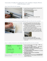
1. Firstly, download ClockBuilder Pro Software (See Figure 2-3), which is
provided by Silicon Labs. This tool can help users to set the Si5341A’s output
frequency of each channel through the GUI interface, and it will automatically
calculate the Register parameters required for each frequency. The tool
download link:
http://url.terasic.com/clockuilder_ro_oftware


Apollo S10 SoM
Demonstration
Manual
11
www.terasic.com
October 14,
2020
Figure 2-4 Define Output Clock Frequencies on ClockBuilder Pro Wizard
3. After the setting is completed, ClockBuilder Pro Wizard generates a Design
Report(text), which contains users setting frequency corresponding register
value (See Figure 2-5).

Apollo S10 SoM
Demonstration
Manual
12
www.terasic.com
October 14,
2020
Figure 2-5 Open Design Report on ClockBuilder Pro Wizard
4. Open Si5341 control IP sub-module “si5341a_i2c_reg_controller.v “ as shown
in Figure 2-6, refer to Design Report parameter to modify sub-module
corresponding register value (See Figure 2-7).
Figure 2-6 Sub-Module file "Si5341A_i2c_reg_controller.v"

Apollo S10 SoM
Demonstration
Manual
13
www.terasic.com
October 14,
2020
Figure 2-7 Modify Si5341A Control IP Base on Design Report
After modifying and compiling, Si5341A can output new frequencies according to the
users’ setting.
Note :
No need to modify all Design Report parameters in si5341a_i2c_reg_controller.v, users
can ignore parameters which have nothing to do with the frequency setting
2.2 Basic Nios II control demo for
SI5341A/ Temperature/ Power/ Fan
This demonstration shows how to use the Nios II processor to program programmable
clock generators (Si5341A) on the FPGA board, how to measure the power
consumption based on the built-in power measure circuit. The demonstration also
includes a function of monitoring system temperature with the on-board temperature
sensor and monitoring fan rotation speed.
System Block Diagram
Figure 2-8 shows the system block diagram of this demonstration. The Si5341A clock
generator is controlled through I2C controllers driven by Nios II program. The 12V input
power monitor, temperature sensor and fan controller connected to the MAX10 FPGA

Apollo S10 SoM
Demonstration
Manual
14
www.terasic.com
October 14,
2020
and controlled by internal logic circuits. All collected status data or control commands
will be sent to the SPI slave block so that the Stratix 10 FPGA can read it through the
SPI interface.
In the Stratix 10 FPGA, an SPI master IP (implemented by HDL) will read these
external sensor data from the MAX10 FPGA through SPI interface. The Nios system
will read these information or output the PLL control settings through PIO controllers.
Figure 2-8 Block Diagram of the Nios II Basic Demonstration
The system provides a menu in nios-terminal, as shown in Figure 2-9 to provide an
interactive interface. With the menu, users can perform the test for the external
programmable PLL and board info sensor. Note, pressing ‘ENTER’ should be followed
with the choice number.

Apollo S10 SoM
Demonstration
Manual
15
www.terasic.com
October 14,
2020
Figure 2-9 Menu of Demo Program
In board info test, the program will display local temperature, remote temperature, 12V
input power monitor and fan rotation speed. The remote temperature is the FPGA
temperature, and the local temperature is the board temperature where the
temperature sensor located. A power monitor IC (LTC2945) embedded on the board
can monitor real-time current and power. This IC can work out current/power value as
multiplier and divider are embedded in it. There is a sense resistor R4 (0.003 Ω) for
LTC2945 in the circuit, when power on the Apollo S10, there will be a voltage drop
(named ∆SENSE Voltage) on R4. Based on sense resistors, the program of power
monitor can calculate the associated voltage, current and power consumption.
In the external PLL programming test, the program will program the PLL first, and
subsequently use TERASIC custom Platform Designer CLOCK_COUNTER IP to count
the clock count in a specified period to check whether the output frequency as changed
as configured. For Si5341A programming, please note the device I2C address is 0xEE.
The program can control the Si5341A to configure the output frequency of
FMC_REFCLK0, FMC_REFCLK1, FMCP_REFCLK0, FMCP_REFCLK1,

Apollo S10 SoM
Demonstration
Manual
16
www.terasic.com
October 14,
2020
FMCP_REFCLK2, DDR4B_REFCLK and LVDS_REFCLK according to your choice.
Demonstration File Location
Hardware project directory: NIOS_BASIC_DEMO
Bitstream used: S10_top.sof
Software project directory: NIOS_BASIC_DEMO\software
Demo batch file: NIOS_BASIC_DEMO\demo_batch\test.bat, test.sh
Demonstration Setup and Instructions
1. Make sure Quartus Prime is installed on the Host PC.
2. Power on the FPGA board.
3. Use the USB Cable to connect your PC and the FPGA board and install USB
Blaster II driver if necessary.
4. Execute the demo batch file “test.bat” under the batch file folder:
NIOS_BASIC_DEMO\demo_batch.
5. After the Nios II program is downloaded and executed successfully, a prompt
message will be displayed in nios2-terminal.
6. For the PLL Si5341A test, please input key ‘0’ and input the desired output
frequency for eight clock sources, as shown in Figure 2-10.


Apollo S10 SoM
Demonstration
Manual
18
www.terasic.com
October 14,
2020
Figure 2-11 Board Info Demo
2.3 DDR4 SDRAM RTL Test
This demonstration performs a memory test function on the DDR4 memory (DDR4A
and DDR4B) on the Apollo S10 SoM board. The memory size of each DDR4 bank
used in this test is 32GB.
Function Block Diagram
Figure 2-12 shows the function block diagram of this demonstration. There are two
DDR4 SDRAM controllers. All of the controllers (DDR4A and DDR4B) use 266.66 MHz
as a reference clock. It generates one 1066MHz clock as memory clock from the FPGA
to the memory and the controller itself runs at quarter-rate in the FPGA i.e. 266.66
MHz.

Apollo S10 SoM
Demonstration
Manual
19
www.terasic.com
October 14,
2020
Figure 2-12 Block diagram of the DDR4 RTL demonstration
Stratix 10 External Memory Interfaces
To use Stratix 10 External Memory Interfaces controller for DDR4 SDRAM, please
perform the two major steps below:
1. Create correct pin assignments for the DDR4 SDRAM.
2. Setup correct parameters in the dialog of the Stratix 10 External Memory
Interfaces.
Design Tools
Quartus Prime 19.4 Pro Edition or later
Demonstration Source Code
Project Directory: Demonstration\FPGA\RTL_DDR4_Test
Bit Stream: S10_top.sof
Demonstration Batch File : RTL_DDR4_Test\demo_batch
The demo batch file includes following files:
Batch File: test.bat
FPGA Configuration File: S10_top.sof
Demonstration Setup
1. Make sure Quartus Prime Pro Edition is installed on the Host PC.
2. Connect the Apollo S10 SoM board to the Host PC via the USB cable. Install the
USB-Blaster II driver if necessary.

Apollo S10 SoM
Demonstration
Manual
20
www.terasic.com
October 14,
2020
3. Power on the Apollo S10 SoM board.
4. Execute the demo batch file “test.bat” under the batch file folder
\RTL_DDR4_Test\demo_batch.
5. Press KEY1 (see Figure 2-13) to start DDR4 write & loopback verify process. It
will take about 2~3 second to perform the test. While testing, the LED will blink.
When LED stop blinking it means the test process is done. In this case, if the LED
light, it means the test result is passed. If the LED is no light, it means the test
result is failed. The LED0 represents the test result for the DDR4A, the LED1
represents the test result for the DDR4B.
6. Press KEY1 again to regenerate the test control signals for a repeat test.
Figure 2-13 Location of the KEY and LED on the Apollo S10 SoM board
2.4 DDR4 SDRAM Test by Nios II
Many applications use a high performance RAM, such as a DDR4 SDRAM, to provide
temporary storage. In this demonstration hardware and software designs are provided
to illustrate how to perform DDR4 memory access in the Platform Designer (formerly
Qsys). We describe how the memory controller Stratix 10 External Memory Interfaces
is used to access the two DDR4 SDRAM banks on the FPGA board, and how the Nios
/