
91250E-UM100-R
16215 Alton Parkway • P.O. Box 57013 • Irvine, CA 92619-7013 • Phone: 949-450-8700 • Fax: 949-450-8710 01/07/05
USER MANUAL
BCM91250E
Evaluation Board

Broadcom
®
and the pulse logo are trademarks of Broadcom Corporation and/or its subsidiaries in the United States and
certain other countries. All other trademarks mentioned are the property of their respective owners.
Broadcom Corporation
P.O. Box 57013
16215 Alton Parkway
Irvine, CA 92619-7013
© 2005 by Broadcom Corporation
All rights reserved
Printed in the U.S.A.
REVISION HISTORY
Revision Date Change Description
91250E-UM100-R 01/07/05 Initial release.

User Manual BCM91250E
01/07/05
Broadcom Corporation
Document 91250E-UM100-R Page iii
TABLE OF CONTENTS
Section 1: Product Overview..............................................................................................1
Introduction .................................................................................................................................................. 1
Items Included with the Shipment.............................................................................................................. 1
Features ........................................................................................................................................................ 1
Hardware ................................................................................................................................................ 1
Firmware................................................................................................................................................. 1
Section 2: Getting Started...................................................................................................3
Section 3: Physical Description .........................................................................................5
Block Diagram.............................................................................................................................................. 5
Pinout For Hypertransport Socket (J3) ................................................................................................... 7
Pinout For Mezzanine Connector (J17) .................................................................................................. 9
ROM Emulator Pinout........................................................................................................................... 11
LEDs............................................................................................................................................................ 12
Fuses and Battery...................................................................................................................................... 14
Switches...................................................................................................................................................... 15
Peripheral Devices..................................................................................................................................... 16
Section 4: Firmware Configuration..................................................................................17
Section 5: Troubleshooting ..............................................................................................18
Corrective Procedures............................................................................................................................... 18
Replacement Parts..................................................................................................................................... 18
Section 6: Web Resources................................................................................................19
SiByte.......................................................................................................................................................... 19
Peripheral Components............................................................................................................................. 19
Bus Interface .............................................................................................................................................. 19

BCM91250E User Manual
01/07/05
Broadcom Corporation
Page iv Document 91250E-UM100-R
LIST OF TABLES
Table 1: Connector Descriptions.........................................................................................................................6
Table 2: Pinout For Hypertransport Socket (J3) .................................................................................................7
Table 3: Pinout For Mezzanine Connector (J17) ................................................................................................9
Table 4: ROM Emulator Pinout.........................................................................................................................11
Table 5: LED Descriptions................................................................................................................................13
Table 6: Fuses and Battery Descriptions..........................................................................................................14
Table 7: Switch Descriptions.............................................................................................................................15
Table 8: SMBus Peripherals .............................................................................................................................16
Table 9: Generic Bus Peripherals.....................................................................................................................16
Table 10: GPIO Map.........................................................................................................................................16
Table 11: PCI Interrupt Map..............................................................................................................................16
Table 12: Firmware Generic Bus Memory Mapping..........................................................................................17
Table 13: Firmware Configuration Bits Mapping...............................................................................................17
Table 14: Replacement Parts ...........................................................................................................................18
Table 15: SiByte Web Resources.....................................................................................................................19
Table 16: Peripheral Component Web Resources ...........................................................................................19
Table 17: Bus Interface Web Resources ..........................................................................................................19

User Manual BCM91250E
01/07/05
Broadcom Corporation
Document 91250E-UM100-R Page v
LIST OF FIGURES
Figure 1: BCM91250E Front View...................................................................................................................... 5
Figure 2: BCM91250E Block Diagram................................................................................................................ 5
Figure 3: Connector Callouts.............................................................................................................................. 6
Figure 4: LED Callouts ..................................................................................................................................... 12
Figure 5: Fuses and Battery Callouts ............................................................................................................... 14
Figure 6: Switch Callouts.................................................................................................................................. 15

BCM91250E User Manual
01/07/05
Broadcom Corporation
Page vi Document 91250E-UM100-R

User Manual BCM91250E
01/07/05
Broadcom Corporation
Document 91250E-UM100-R Product Overview Page 1
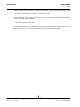
Section 1: Product Overview
INTRODUCTION
The BCM91250E evaluation board is an evaluation platform intended to support the needs of prospective
users of the BCM1250 processor. This user manual provides information on how to get the BCM91250E
evaluation board up and running quickly. This manual also describes how to locate, configure, and observe
the various connectors, switches, jumpers, and LEDs on the BCM91250E, allowing software development and
evaluation of the BCM1250 processor to begin.
For additional information on this board and the BCM1250 processor, go to:
http://sibyte.broadcom.com/public.
ITEMS INCLUDED WITH THE SHIPMENT
The following items are included with the BCM91250E evaluation board shipment:
• BCM91250E evaluation board
• This document
FEATURES
This section describes the BCM91250E’s features.
HARDWARE
• BCM1250 processor
• Full length PCI card form factor
• 256 MB DDR SDRAM
• Two 10/100/1000 Mbps Ethernet interfaces with RJ45 connectors
• One UART with RS232 interface
• Universal 32-bit, 33/66-MHz capable PCI connector
• 2 MB Flash ROM
• Two SMBus channels with the following devices connected:
-RTC
- EEPROM
- Temperature sensor
• EJTAG connector
• PROMICE connector
FIRMWARE
The Common Firmware Environment (CFE) is designed to be easily portable to designs incorporating current
and future Broadcom MIPS64-compatible broadband processors. Supported platforms include Broadcom’s

BCM91250E User Manual
01/07/05
Broadcom Corporation
Page 2 Features Document 91250E-UM100-R
SiByte processor family (containing the BCM1250, BCM1125H, and other processors), 32-bit and 64-bit
memory models, and big and little-endian operation. There are many parameters configurable at build time that
can be used to customize CFE to suit diverse customer requirements.
On the BCM91250E, CFE can load programs (such as S-records, raw binary, or ELF formatted) from bootstrap
devices in a variety of ways, including:
• Via either Ethernet port, from a TFTP server
• Via the serial port (S-records only)
For additional information on CFE, refer to the Common Firmware Environment (CFE) Specification document
that can be found in the CFE source code distribution at: http://sibyte.broadcom.com/public.

User Manual BCM91250E
01/07/05
Broadcom Corporation
Document 91250E-UM100-R Getting Started Page 3
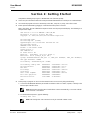
Section 2: Getting Started
Complete the following steps to get to a BCM91250E CFE (firmware) prompt.
1 Connect a 9-pin null modem cable to the serial port of the BCM91250E and to a serial port on a workstation/PC.
2 Use a terminal program and set it to 115200 bps, 8-bit data, 1-stop bit, no parity, and no flow control.
3 Power up the BCM91250E by plugging in a standard hard drive power connector.
After a short delay, the CFE initialization output and serial console prompt should display. The following is an
example of the output:
CFE version 1.0.37 for SENTOSA (64bit,MP,BE)
Build Date: Fri Jul 11 10:40:26 PDT 2003
Copyright (C) 2000,2001,2002,2003 Broadcom Corporation.
Initializing Arena.
Initializing PCI. [normal]
HyperTransport not initialized: InitDone not set
Initializing Devices.
SENTOSA board revision 1
PCIIDE: 0 controllers found
Config switch: 2
CPU: BCM1250 B2
L2 Cache Status: OK
Wafer ID: 0x2164E019 [Lot 2137, Wafer 7]
Manuf Test: Bin A [2CPU_FI_FD_F2 (OK)]
SysCfg: 0000000020C20800 [PLL_DIV: 16, IOB0_DIV: CPUCLK/4, IOB1_DIV: CPUCLK/3]
CPU type 0x1040102: 800MHz
Total memory: 0x10000000 bytes (256MB)
Total memory used by CFE: 0x8FE8C880 - 0x90000000 (1521536)
Initialized Data: 0x8FE8C880 - 0x8FE964A0 (39968)
BSS Area: 0x8FE964A0 - 0x8FE96B90 (1776)
Local Heap: 0x8FE96B90 - 0x8FF96B90 (1048576)
Stack Area: 0x8FF96B90 - 0x8FF98B90 (8192)
Text (code) segment: 0x8FF98BA0 - 0x8FFFFFB0 (422928)
Boot area (physical): 0x0FE4B000 - 0x0FE8B000
Relocation Factor: I:F0398BA0 - D:0DF8C880
CFE>
4 At the prompt, a program can be run via the network from a TFTP server by doing the following:
a. Connect the BCM91250E Ethernet port E0 with an Ethernet cable to a switch, repeater, or directly to the
Ethernet port of the file server.
b. To initialize Ethernet port E0, type the following:
ifconfig eth0 -auto
Note: Because the Broadcom PHYs handle direct connects automatically, a crossover cable for
direct connects is not needed.
Note: The ifconfig eth0 -auto command can only be used with a DHCP server.

BCM91250E User Manual
01/07/05
Broadcom Corporation
Page 4 Getting Started Document 91250E-UM100-R
c. To run a program, type the following:
boot -elf tftp_server:/path_to_software/program

User Manual BCM91250E
01/07/05
Broadcom Corporation
Document 91250E-UM100-R Physical Description Page 5
Section 3: Physical Description
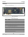
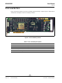
The BCM91250E is implemented in the standard full length PCI card form factor. Figure 1 shows a front view
of the BCM91250E.
Figure 1: BCM91250E Front View
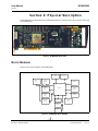
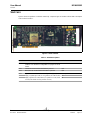
BLOCK DIAGRAM
Figure 2 shows a block diagram of the BCM91250E.
Figure 2: BCM91250E Block Diagram
BCM1250
HT
Connector
128 MB
DDR SDRAM
128 MB
DDR SDRAM
Serial
Port S0
EJTAG
PROMICE
Connector
Flash
ROM
PCI
Connector
10/100/1000
Ethernet
Port E0
10/100/1000
Ethernet
Port E1
Mezzanine
Connector
RTC
EEPROM
E0
E1
8b HT
M0
M1
Temp
Sensor
JTAG
S0
IO_AD
32b PCI
SMBus0
SMBus1
E2
S1/GPIO

BCM91250E User Manual
01/07/05
Broadcom Corporation
Page 6 Connectors Document 91250E-UM100-R
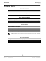
CONNECTORS
Figure 3 shows the board and identifies connectors numerically. For a description of each connector callout,
compare Figure 3’s number callouts with Table 1.
Figure 3: Connector Callouts
The following table shows the BCM91250E connectors.
Table 1: Connector Descriptions
Board ID Description
J2 Dual-sided 62-pin edge finger PCI connector.
J3 HyperTransport socket for motherboards (see Table 2 on page 7).
J8 Serial port 0 RS-232 connector.
J11 ROM emulator connector (see Table 4 on page 11).
J12 ROM emulator write line (pin1* = IO_WR_L, pin2 = no connect).
J14 DEBUG_L trigger for scope (pin1* = GND, pin2 = DEBUG_L).
J15 EJTAG connector.
J17 Mezzanine connector (see Table 3 on page 9).
J18 1.2V core supply sense (pin1* = GND, pin2 = 1.2V).
J19 Standard hard drive power supply connector.
J20 1.2V HyperTransport supply sense (pin1 = GND, pin2 = 1.2V).
J21 2.5V supply sense (pin1* = GND, pin2 = 2.5V).
J22 3.3V supply sense (pin1* = GND, pin2 = 3.3V).
J23A 10/100/1000 Mbps Ethernet Port E1.
J23B 10/100/1000 Mbps Ethernet Port E0.
J63 12V Heatsink/Fan Power (pin1* = 12V, pin2 = GND).
* = Pin1 located by viewing the back of the board for the square solder pad.

User Manual BCM91250E
01/07/05
Broadcom Corporation
Document 91250E-UM100-R Connectors Page 7
PINOUT FOR HYPERTRANSPORT SOCKET (J3)
Note: The table layout reflects the physical location of the pins on the connector. The middle pins
(121-132) are not shown though since they are all connected to ground (GND).
More information about these connectors can be found in “Web Resources” on page 19.
Table 2: Pinout For Hypertransport Socket (J3)
Odd Pin Name
Odd Pin
Number
Even Pin
Number
Even Pin Name
VDD33 1 2 VDD33
VDD33 3 4 VDD33
VDDLDT 5 6 VDDLDT
GND 7 8 GND
TCK 9 10 CLK100
TMS 11 12 GND
TDI 13 14 RDY
TDO 15 16 OE_L
TRST_L 17 18 WR_L
SCL 19 20 CS_L0
SDA 21 22 CS_L1
LDT_RESET_L 23 24 INT
LDT_PWROK 25 26 RESET_L
GND 27 28 GND
LDT_RX_CTLn 29 30 LDT_TX_CADp0
LDT_RX_CTLp 31 32 LDT_TX_CADn0
GND 33 34 GND
LDT_RX_CADn7 35 36 LDT_TX_CADp1
LDT_RX_CADp7 37 38 LDT_TX_CADn1
GND 39 40 GND
GND 41 42 GND
LDT_RX_CADn6 43 44 LDT_TX_CADp2
LDT_RX_CADp6 45 46 LDT_TX_CADn2
GND 47 48 GND
LDT_RX_CADn5 49 50 LDT_TX_CADp3
LDT_RX_CADp5 51 52 LDT_TX_CADn3
GND 53 54 GND
LDT_RX_CADn4 55 56 LDT_TX_CLKp
LDT_RX_CADp4 57 58 LDT_TX_CLKn
GND 59 60 GND

BCM91250E User Manual
01/07/05
Broadcom Corporation
Page 8 Connectors Document 91250E-UM100-R
GND 61 62 GND
LDT_RX_CLKn 63 64 LDT_TX_CADp4
LDT_RX_CLKp 65 66 LDT_TX_CADn4
GND 67 68 GND
LDT_RX_CADn3 69 70 LDT_TX_CADp5
LDT_RX_CADp3 71 72 LDT_TX_CADn5
GND 73 74 GND
LDT_RX_CADn2 75 76 LDT_TX_CADp6
LDT_RX_CADp2 77 78 LDT_TX_CADn6
GND 79 80 GND
GND 81 82 GND
LDT_RX_CADn1 83 84 LDT_TX_CADp7
LDT_RX_CADp1 85 86 LDT_TX_CADn7
GND 87 88 GND
LDT_RX_CADn0 89 90 LDT_TX_CTLp
LDT_RX_CADp0 91 92 LDT_TX_CTLn
GND 93 94 GND
AD0 95 96 AD9
AD1 97 98 AD24
AD2 99 100 AD25
AD3 101 102 AD26
AD4 103 104 AD27
AD5 105 106 AD28
AD6 107 108 AD29
AD7 109 110 AD30
AD8 111 112 AD31
GND 113 114 GND
VDDLDT 115 116 VDDLDT
VDD33 117 118 VDD33
VDD33 119 120 VDD33
Table 2: Pinout For Hypertransport Socket (J3) (Cont.)
Odd Pin Name
Odd Pin
Number
Even Pin
Number
Even Pin Name

User Manual BCM91250E
01/07/05
Broadcom Corporation
Document 91250E-UM100-R Connectors Page 9
PINOUT FOR MEZZANINE CONNECTOR (J17)
Note: The table layout reflects the physical location of the pins on the connector. The middle pins
(121-132) are not shown though since they are all connected to ground (GND).
More information about these connectors can be found in “Web Resources” on page 19.
Table 3: Pinout For Mezzanine Connector (J17)
Odd Pin Name
Odd Pin
Number
Even Pin
Number
Even Pin Name
VDD33 1 2 VDD33
VDD33 3 4 VDD33
VDD50 5 6 VDD50
GND 7 8 GND
E2_RCLK 9 10 E2_TCLKI
GND 11 12 GND
E2_RXD7 13 14 E2_TCLKO
GND 15 16 GND
E2_RXD6 17 18 E2_TXD7
GND 19 20 GND
E2_RXD5 21 22 E2_TXD6
GND 23 24 GND
E2_RXD4 25 26 E2_TXD5
GND 27 28 GND
E2_RXD3 29 30 E2_TXD4
GND 31 32 GND
E2_RXD2 33 34 E2_TXD3
GND 35 36 GND
E2_RXD1 37 38 E2_TXD2
GND 39 40 GND
E2_RXD0 41 42 E2_TXD1
GND 43 44 GND
E2_RXDV 45 46 E2_TXD0
GND 47 48 GND
E2_RXER 49 50 E2_TXEN
GND 51 52 MEZ_MAC_PRSNT_L
E2_COL 53 54 E2_TXER
GND 55 56 GND
E2_CRS 57 58 E2_MDC
GND 59 60 GND

BCM91250E User Manual
01/07/05
Broadcom Corporation
Page 10 Connectors Document 91250E-UM100-R
E2_MDIO 61 62 REFCLK02
GND 63 64 GND
IO_RD_WR 65 66 GPIO15
IO_CS_L3 67 68 GPIO14
IO_CS_L4 69 70 GPIO13
IO_ALE 71 72 GPIO12
GND 73 74 GPIO11
S1_DIN 75 76 GPIO10
S1_DIN_RCLKIN 77 78 GPIO9
S1_CTS_TCLKIN 79 80 GPIO8
S1_RIN 81 82 GND
GND 83 84 GPIO7
S1_TIN 85 86 GPIO6
S1_DOUT 87 88 GPIO5
S1_COUT 89 90 GPIO4
S1_RTS_TSTROBE 91 92 GPIO3
GND 93 94 GPIO2
IO_AD10 95 96 GPIO1
IO_AD11 97 98 GPIO0
IO_AD12 99 100 GND
IO_AD13 101 102 IO_AD14
GND 103 104 IO_AD16
IO_AD15 105 106 IO_AD18
IO_AD17 107 108 IO_AD20
IO_AD19 109 110 IO_AD22
IO_AD21 111 112 IO_AD23
GND 113 114 VDDN120
VDD50 115 116 VDD50
VDD33 117 118 VDD120
VDD33 119 120 VDD120
Table 3: Pinout For Mezzanine Connector (J17) (Cont.)
Odd Pin Name
Odd Pin
Number
Even Pin
Number
Even Pin Name

User Manual BCM91250E
01/07/05
Broadcom Corporation
Document 91250E-UM100-R Connectors Page 11
ROM EMULATOR PINOUT
Note: The table layout reflects the physical location of the pins on the connector. Also all I/O
signals are 3.3 V outputs that are tolerant of 5V inputs.
Table 4: ROM Emulator Pinout
Odd Pin Name Odd Pin Number
Even Pin
Number
Even Pin Name
GND 1 2 AD20
3.3 V PWR 3 4 AD19
AD18 5 6 AD16
AD17 7 8 AD15
AD14 9 10 AD12
AD13 11 12 AD7
AD81314AD6
AD91516AD5
AD11 17 18 AD4
OE_L 19 20 AD3
AD10 21 22 AD2
ROMEMUCS_L 23 24 AD1
AD31 25 26 AD0
AD30 27 28 AD24
AD29 29 30 AD25
AD28 31 32 AD26
AD27 33 34 GND


User Manual BCM91250E
01/07/05
Broadcom Corporation
Document 91250E-UM100-R LEDs Page 13
Table 5: LED Descriptions
Board ID Color Description
D1 Red 2.5V Fuse blown indicator
D2 Red 3.3V Fuse blown indicator
D7 * Ethernet Port E1 PHY LEDs
Red Link2 = Speed indicator.
Green Link1 = Speed indicator.
Yellow Fdx = Full-duplex indicator.
Green Slv = Slave indicator.
Yellow Act = Transmit and receive activity indicator.
Green Link = Link quality indicator.
D12 * Ethernet Port E0 PHY LEDs
Red Link2 = Speed indicator.
Green Link1 = Speed indicator.
Yellow Fdx = Full-duplex indicator.
Green Slv = Slave indicator.
Yellow Act = Transmit and receive activity indicator.
Green Link = Link quality indicator.
D13 Green Debug LED.
D16 Green 3.3V power good.
D18 Green 5V.
* = LEDs visible from the board’s side panel.

BCM91250E User Manual
01/07/05
Broadcom Corporation
Page 14 Fuses and Battery Document 91250E-UM100-R
FUSES AND BATTERY
Figure 5 shows the positions of the fuses and battery alpha-numerically. Compare Figure 5’s alpha-numeric
callouts with a description of each fuse or battery in Table 6.
Figure 5: Fuses and Battery Callouts
.
Table 6: Fuses and Battery Descriptions
Board ID Function
F1 BCM1250 2.5V current limit, 5A.
F2 BCM1250 3.3V current limit, 1A.
F3 EJTAG 3.3V, 1A current limit fuse.
BT1 RTC battery.
Page is loading ...
Page is loading ...
Page is loading ...
Page is loading ...
Page is loading ...
Page is loading ...
-
 1
1
-
 2
2
-
 3
3
-
 4
4
-
 5
5
-
 6
6
-
 7
7
-
 8
8
-
 9
9
-
 10
10
-
 11
11
-
 12
12
-
 13
13
-
 14
14
-
 15
15
-
 16
16
-
 17
17
-
 18
18
-
 19
19
-
 20
20
-
 21
21
-
 22
22
-
 23
23
-
 24
24
-
 25
25
-
 26
26


Broadcom 91250E-UM100-R.pdf User manual
- Type
- User manual
- This manual is also suitable for
Ask a question and I''ll find the answer in the document
Finding information in a document is now easier with AI
Related papers
-
LSI BCM91125E User manual
-
Broadcom BCM1250; BCM1125H; BCM1122 User guide
-
-
-
-
Broadcom 91125F-UM100-R.pdf User manual
-
-
-
-
Other documents
-
Clatronic BSS 7013 User manual
-
Solar CFE-5100S User manual
-
Panasonic CZ-CFUNC1U Installation guide
-
CFE S Pro Series User manual
-
 Tundra TSI308 User manual
-
Flomec QSE Mag Flow Meter Owner's manual
-
HP PageWide Managed Color MFP E77650-E77660 Printer series User guide
-
Maxim 58740 Wafer 22 Inch RD LED Surface Mount 4000K Installation guide
-
 Futuredesign controls UM100 User manual
-
 Lutron Electronics QSE-CI-NWK-E User manual


