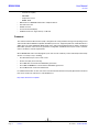
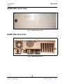
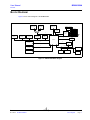
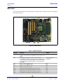
Broadcom 91250A-UM100-R.pdf is a user manual that provides detailed instructions and information on the features and capabilities of the BCM91250A evaluation board. This evaluation board is designed to showcase the capabilities of the BCM91250A system-on-a-chip (SoC), which is a highly integrated device that combines a MIPS32 4KEc processor core, a HyperTransport 1.0/1.1 interface, an I/O bridge, and other peripherals. The BCM91250A SoC is designed for use in a wide range of embedded applications, including networking, storage, and industrial automation.
The BCM91250A evaluation board provides a comprehensive platform for evaluating the capabilities of the BCM91250A SoC. The board includes a variety of features, including:
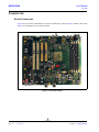
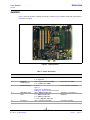


-
 1
1
-
 2
2
-
 3
3
-
 4
4
-
 5
5
-
 6
6
-
 7
7
-
 8
8
-
 9
9
-
 10
10
-
 11
11
-
 12
12
-
 13
13
-
 14
14
-
 15
15
-
 16
16
-
 17
17
-
 18
18
-
 19
19
-
 20
20
-
 21
21
-
 22
22
-
 23
23
-
 24
24
-
 25
25
-
 26
26
-
 27
27
-
 28
28
-
 29
29
-
 30
30
-
 31
31
-
 32
32
-
 33
33
-
 34
34


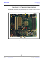
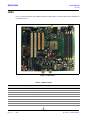
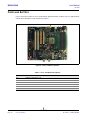
Broadcom 91250A-UM100-R.pdf is a user manual that provides detailed instructions and information on the features and capabilities of the BCM91250A evaluation board. This evaluation board is designed to showcase the capabilities of the BCM91250A system-on-a-chip (SoC), which is a highly integrated device that combines a MIPS32 4KEc processor core, a HyperTransport 1.0/1.1 interface, an I/O bridge, and other peripherals. The BCM91250A SoC is designed for use in a wide range of embedded applications, including networking, storage, and industrial automation.
The BCM91250A evaluation board provides a comprehensive platform for evaluating the capabilities of the BCM91250A SoC. The board includes a variety of features, including:
Ask a question and I''ll find the answer in the document
Finding information in a document is now easier with AI
Related papers
-
Broadcom BCM1250; BCM1125H; BCM1122 User guide
-
-
LSI BCM91125E User manual
-
-
-
Broadcom 91125F-UM100-R.pdf User manual
-
-
-
-

