
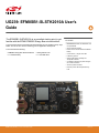
UG239: EFM8SB1-SLSTK2010A User's
Guide
The EFM8SB1-SLSTK2010A is an excellent starting point to get
familiar with the EFM8 EFM8SB1 Sleepy Bee microcontrollers.
The kit contains sensors and peripherals demonstrating some of the MCU's many capa-
bilities. The kit can also serve as a starting point for application development.
The kit includes the following:
KEY FEATURES
• EFM8SB10F8G MCU with 8 kB Flash and
512 bytes RAM.
• 20-pin expansion header.
• Power sources include USB and CR2032
battery.
• 2 user buttons, 1 single-color LED.
• 8-direction joystick.
• Silicon Labs Si7021 Humidity and
Temperature Sensor.
• 4 Capacitive Sense touch pads arranged
as a wheel and button.
• 32 kHz crystal for the RTC.
• Ultra low power 128x128 pixel Memory-
LCD.
• EFM8SB1 Sleepy Bee Starter Kit Board
• 1 x CR2032 battery
• Getting Started card
• 1 x mini USB cable
silabs.com | Building a more connected world. Rev. 0.3

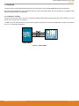
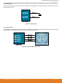
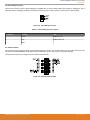
1. Getting Started
Hardware
To set up the hardware for the EFM8SB1-SLSTK2010A kit:
1. Provide power to the board by connecting the USB connector to the PC using the provided USB cable.
2. Move the switch to the Advanced Energy Monitor (AEM) position.
Figure 1.1. Hardware Setup
Software
The first step to get started with your new EFM8SB1-SLSTK2010A is to go to
http://www.silabs.com/simplicity
The Simplicity Studio software package contains all the tools, drivers, software examples and documentation needed to use the
EFM8SB1 Starter Kit. The board comes pre-loaded with a default application, Clock, to interact with while the software downloads.
After downloading the latest version of Simplicity Studio and installing:
1. Select the J-Link adapter for the kit under [Devices].
2. Click one of the demos available under [Getting Started]>[Demos] or click the [Getting Started]>[Demos]>[View All] to view the
entire list of available demos.
3. Click the [PWM Blinky] demo and click [Start] to download and run the demo.
Additional demos showcasing the various features of the EFM8 are also available in Simplicity Studio.
UG239: EFM8SB1-SLSTK2010A User's Guide
Getting Started
silabs.com | Building a more connected world. Rev. 0.3 | 2

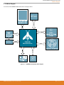
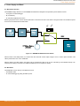
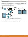
2. Kit Block Diagram
An overview of the EFM8SB1 Starter Kit is shown in the figure below.
ADC
I2C / SMBus
Joystick
EFM8SB1
Microcontroller
CS0
GPIO
POWER
Board
Controller
UART
Figure 2.1. EFM8SB1-SLSTK2010A Block Diagram
UG239: EFM8SB1-SLSTK2010A User's Guide
Kit Block Diagram
silabs.com | Building a more connected world. Rev. 0.3 | 3

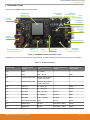
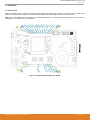
3. Kit Hardware Layout
The layout of the EFM8SB1 Starter Kit is shown below.
Kit USB
Connector
CR2032
Battery Holder
Power Source Select
User Push
Buttons
User LED
EFM8 Reset Button
EFM8SB1 MCU
Expansion
Header
Joystick
128x128 Pixel
Memory LCD
Capacitive
Touch Pads
Humidity and
Temp Sensor
Direct
Debug Connector
Debug IN/OUT
Connector
Reference
Board Connector
Figure 3.1. EFM8SB1-SLSTK2010A Hardware Layout
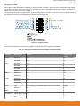
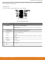
The EFM8 device on the kit is connected to several peripherals. The table below shows all of the external connections to the MCU.
Table 3.1. Kit MCU Connections
MCU Port Pin Port Pin Assigned
Function
Primary Board Connec-
tion
Secondary Board Con-
nection
Expansion Port Con-
nection (EXP)
P0.0 GPIO BC - Enable
P0.1 GPIO DISP - SPI CS EXP3
P0.2 Capacitive Sense Input Capacitive Sense Button
1 (part of the wheel)
P0.3 Capacitive Sense Input Capacitive Sense Button
2 (part of the wheel)
P0.4 UART0 TX BC - UART_TX EXP12
P0.5 UART0 RX BC - UART_RX EXP14
P0.6 SPI0 SCK
DISP - SPI CLK
4
SPI CLK EXP8
P0.7 SPI0 MISO BC - REFCLK SPI MISO EXP6
P1.0 SPI0 MOSI DISP - SPI MOSI SPI MOSI EXP4
P1.1 PCA0 CEX0 / SPI0 NSS LED0 SPI CS EXP10
P1.2 SMBus0 SDA I2C SDA
Push Button 0 (PB0)
1
EXP16
P1.3 SMBus0 SCL I2C SCL
Push Button 1 (PB1)
1
EXP15
UG239: EFM8SB1-SLSTK2010A User's Guide
Kit Hardware Layout
silabs.com | Building a more connected world. Rev. 0.3 | 4

MCU Port Pin Port Pin Assigned
Function
Primary Board Connec-
tion
Secondary Board Con-
nection
Expansion Port Con-
nection (EXP)
P1.4 ADC Joystick Capacitive Sense Button
c (center button inside
the wheel)
2
P1.5 Capacitive Sense Input Capacitive Sense Button
3 (part of the wheel)
P1.6 XTAL3 32 kHz crystal
EXP5
3
P1.7 XTAL4 32 kHz crystal
EXP7
3
P2.7 / C2D GPIO / C2D (for debug) Debug - C2D DISP - Enable
Note:
1. The pushbuttons are connected by default to the I2C bus connected to the Si7021 humidity sensor and the EXP header. Pressing
a button during a transfer will interrupt the transfer.
2. The center Capacitive Sense button is not connected by default to P1.4. Instead, this pin is connected to the joystick. The board
has an unpopulated 0 Ω resistor that can be used to connect the center button.
3. These pins are not connected to the expansion header by default. The board has 0 Ω resistors that can be moved to connect
these signals to these pins.
4. This signal has high loading. If the MCU pin is used for signals where edge speed is critical, this signal should be disconnected
from the pin.
UG239: EFM8SB1-SLSTK2010A User's Guide
Kit Hardware Layout
silabs.com | Building a more connected world. Rev. 0.3 | 5

4. Power Supply and Reset
4.1 MCU Power Selection
The EFM8SB1 Sleepy Bee MCU on the EFM8SB1-SLSTK2010A is designed to be powered by three different sources:
• Through the on-board debugger.
• By a 3 V Battery.
• An externally supplied power source.
Selecting the power source is done with the slide switch in the lower left corner of the board. The figure shows how the different power
sources can be selected with the slide switch.
AEM
BAT
8
AEM
BAT
Figure 4.1. EFM8SB1-SLSTK2010A Power Switch
With the switch in the AEM position, an on-board low noise LDO with a fixed output voltage of 3.3 V is used to power the MCU. This
LDO is powered from the "J-Link" USB cable.
With the switch in the BAT position, the device may be powered from either a 20 mm coin cell battery (in the CR2032 socket) or an
external power supply (connected to the VMCU and GND pins on the expansion header).
4.2 MCU Reset
The EFM8 MCU can be reset by a few different sources:
• The RESET button.
• An external debugger by pulling the RSTb pin low.
UG239: EFM8SB1-SLSTK2010A User's Guide
Power Supply and Reset
silabs.com | Building a more connected world. Rev. 0.3 | 6

5. Peripherals
The starter kit has a set of peripherals that showcase some of the features of the EFM8 EFM8SB1 Sleepy Bee microcontroller.
Be aware that most EFM8 I/O routed to peripherals are also routed to the breakout pads. This must be taken into consideration when
using the breakout pads for your application.
5.1 Push Buttons and LEDs
The kit has two user push buttons. They are connected to the EFM8, and are debounced by RC filters with a time constant of 1 ms. The
buttons are connected to pins P1.2 and P1.3.
In addition to the two push buttons, the kit also features a single-color LED that is controlled by EFM8 GPIO. The LED is connected to
pin P1.1 in an active-high configuration.
Figure 5.1. Buttons/LEDs
UG239: EFM8SB1-SLSTK2010A User's Guide
Peripherals
silabs.com | Building a more connected world. Rev. 0.3 | 7

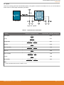
5.2 Joystick
The kit has an analog joystick with 8 measureable positions. This joystick is connected to the EFM8 on the P1.4 pin and uses different
resistor values to create voltages measurable by the ADC0.
Figure 5.2. Joystick
Table 5.1. Joystick Resistor Combinations
Direction Resistors Combinations (kΩ)
Expected UIF_JOYSTICK Voltage (V)
1
Center press
0.1
0.1
+ 10
0.033
Up (N)
60.4
60.4 + 10
2.831
Up-Right (NE)
(N // E )
(N // E ) + 10
=
21.34
21.34 + 10
2.247
Right (E)
33
33
+ 10
2.533
Down-Right (SE)
(S // E )
(S // E ) + 10
=
7.67
7.67 + 10
1.433
Down (S)
10
10
+ 10
1.650
Down-Left (SW)
(S // W )
(S // W ) + 10
=
6
6 + 10
1.238
Left (W)
15
15
+ 10
1.980
Up-Left (NW)
(N // W )
(N // W ) + 10
=
12.01
12.01 + 10
1.801
Note:
1. These calculated values assume a VMCU of 3.3 V.
UG239: EFM8SB1-SLSTK2010A User's Guide
Peripherals
silabs.com | Building a more connected world. Rev. 0.3 | 8

5.3 Memory LCD-TFT Display
A 1.28-inch SHARP Memory LCD-TFT has been added to the board to enable interactive applications to be developed. The display has
a high resolution of 128 by 128 pixels and consumes very little power. It is a reflective monochrome display, so each pixel can only be
light or dark, and no backlight is needed in normal daylight conditions.
The display interface consists of an SPI-compatible serial interface and some extra control signals. Data are sent to the display one line
(128 bits) at a time.
The Memory LCD-TFT display is shared with the kit Board Controller, allowing the Board Controller application to display useful infor-
mation when the user application is not using the display. The EFM8 MCU always controls ownership of the display using the
EFM_DISP_ENABLE signal:
• 0: The Board Controller has control of the display.
• 1: The user application (EFM8) has control of the display.
Data are clocked in on EFM_DISP_MOSI (P1.0) when EFM_DISP_CS (P0.1) is high, and the clock is sent on EFM_DISP_SCLK
(P0.6). The maximum supported clock speed is 1 MHz.
Please refer to the display application information for details on driving the display:
http://www.sharpmemorylcd.com/1-28-inch-memory-lcd.html
0: BC controls display
1: EFM controls display
EFM_DISP_ENABLE
8
P0.6 (SPI0)
P1.0 (SPI0)
P0.1 (GPIO)
P2.7 (GPIO)
Figure 5.3. 128x128 Pixel Memory LCD
5.4 Humidity and Temperature Sensor
The EFM8SB1-SLSTK2010A board includes a Silicon Labs Si7021 humidity and temperature sensor to enable datalogging applica-
tions. The EFM8 MCU communicates with this sensor over the I2C / SMBus hardware interface.
Figure 5.4. Humidity and Temperature Sensor
UG239: EFM8SB1-SLSTK2010A User's Guide
Peripherals
silabs.com | Building a more connected world. Rev. 0.3 | 9

5.5 32 kHz Crystal
The kit has a 32 kHz crystal connected to the RTC crystal pins on the EFM8 MCU. This crystal enables the low power modes on the
MCU that utilize the RTC.
Figure 5.5. 32 kHz Crystal
5.6 Capacitive Sense
The EFM8 MCU is connected to capacitive sense pads to enable button and slider applications using the Silicon Labs capacitive sense
firmware library and Capacitive Sense Profiler software included in Simplicity Studio.
Figure 5.6. Capacitive Sense Touch Pads
UG239: EFM8SB1-SLSTK2010A User's Guide
Peripherals
silabs.com | Building a more connected world. Rev. 0.3 | 10

6. Connectors
6.1 Breakout Pads
Many of the EFM8's pins are routed out to "breakout pads" at the top and bottom edges of the kit. A 2.54 mm pitch pin header can be
soldered in for easy access to these pins. Most I/O pins are available, with the exception of pins used to drive the LCD.
Note: Some of the breakout pads are shared by on-board EFM peripherals. The schematic must be consulted to make sure that it is
acceptable to use a shared pin in your application.
P0.0
P0.1
P0.2
P0.3
P0.5
P0.6
P0.7
P1.0
P1.1
P1.2
P1.3
P0.4
P2.7
P1.7
P1.6
P1.5
P1.4
VMCU
Figure 6.1. Breakout Pads and Expansion Header
UG239: EFM8SB1-SLSTK2010A User's Guide
Connectors
silabs.com | Building a more connected world. Rev. 0.3 | 11

6.2 Expansion Header
On the right hand side of the board an angled 20-pin expansion header is provided to allow connection of peripherals or plugin boards.
The connecter contains a number of I/O pins that can be used with most of the EFM8SB1 Sleepy Bee's features. Additionally, the
VMCU, 3V3 and 5V power rails are also exported.
The figure below shows the pin assignment of the expansion header. With the exception of a few pins, most of the expansion header's
pins are the same as those on the EFM32 Gecko or EFM32 Tiny Gecko starter kits.
Figure 6.2. Expansion Header
Some of the chip peripheral functions that are available on the expansion header are listed in the table below.
Table 6.1. Some of the Peripheral Functions Available on Expansion Header
Peripheral Peripheral pin MCU Pin EXP Header pin
number
UART0 UART0 TX P0.4 12
UART0 RX P0.5 14
SPI0 SPI0 SCK P0.6 8
SPI0 MISO P0.7 6
SPI0 MOSI P1.0 4
SPI0 CS P1.1 10
SMBus SMBus0 SDA P1.2 16
SMBus0 SCL P1.3 15
PCA0 PCA0 CEX0 P1.1 10
PCA0 CEX1 P1.6 5
PCA0 CEX2 P1.7 7
ADC0 Input Any supported pin (see Reference Manual for more information) Multiple
CNVSTR P0.6 8
IREF0 Output P0.7 6
Comparator 0 CMP0P Positive Input P1.0 4
CMP0N Negative In-
put
P1.1 10
UG239: EFM8SB1-SLSTK2010A User's Guide
Connectors
silabs.com | Building a more connected world. Rev. 0.3 | 12

Note: This table only sums up some of the alternate functions available on the expansion header. Consult the EFM8SB10F8G data
sheet for a complete list of alternate functions.
6.3 Debug Connector
This connector is used for Debug In and Debug Out (see chapter on Debugging).
Figure 6.3. Debug Connector
Table 6.2. Debug Connector Pinout
Pin num-
ber
Function Note
1 VTARGET Target voltage on the debugged application.
Note: This connection is required and is needed for the debug circuitry to match voltage levels
with the target device.
2 TMS/SWDIO/C2D JTAG TMS, Serial Wire data I/O, or EFM8 C2 data I/O
4 TCK/SWCLK/C2CK JTAG TCK, Serial Wire clock, or EFM8 C2 clock
6 TDO/SWO JTAG TDO or Serial Wire Output
8 TDI JTAG data in
9 ATTACH This signal must be pulled to ground by the external debugger or application for cable insertion
detection.
10 #RESET Target MCU reset.
12 TRACECLK Trace clock
14, 16,
18, 20
TRACED0-3 Trace data (4 lines)
11, 13 NC Not Connected
3, 5, 15,
17, 19
GND
UG239: EFM8SB1-SLSTK2010A User's Guide
Connectors
silabs.com | Building a more connected world. Rev. 0.3 | 13

6.4 Direct Debug Connector
This connector (J103) is used for directly debugging the EFM8 using an external debug adapter (see chapter on Debugging). This is
especially useful for debugging the MCU on the STK board when the part is battery powered or powered by an external supply.
1
3
C2CK
C2D
Figure 6.4. Direct Debug Connector
Table 6.3. Direct Debug Connector Pinout
Pin number Function Note
1 C2CK EFM8 C2 clock
2 C2D EFM8 C2 data I/O
3 GND
6.5 Reference Board
The top-right corner of the board includes a 20-pin reference board connector. The connecter contains some I/O pins that can be used
with some of the EFM8 EFM8SB1 Sleepy Bee's features. Additionally, the 3V3 and 5V power rails are also exported.
The figure below shows the pin assignment of the reference board header.
Figure 6.5. Reference Board Header
UG239: EFM8SB1-SLSTK2010A User's Guide
Connectors
silabs.com | Building a more connected world. Rev. 0.3 | 14

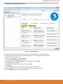
7. Integrated Development Environment
Figure 7.1. Simplicity Studio
Simplicity Studio includes various examples in source form to use with the Starter Kit. To run these examples:
1. Provide power to the board by connecting the DBG USB connector to the PC using the provided USB cable.
2. Move the switch to the AEM position.
3. Select the J-Link adapter for the kit under [Devices].
4. Click the [Getting Started]>[New Project] button.
5. In the wizard, ensure the EFM8SB1 Sleepy Bee Starter Kit Board kit and click [Next].
6. Select [Example] and click [Next].
7. Select the desired example or demo from the list and click [Next].
8. Click [Finish].
9. Click the [Debug] button in the IDE to build and download the code to the hardware.
10. Follow the instructions at the top of the main example file to set up the hardware as needed.
11. Click the [Resume] button to start running the example.
UG239: EFM8SB1-SLSTK2010A User's Guide
Integrated Development Environment
silabs.com | Building a more connected world. Rev. 0.3 | 15

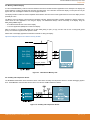
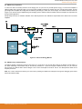
8. Advanced Energy Monitor
When the EFM8SB1 Starter Kit is connected to a Silicon Labs STK, the STK's Advanced Energy Monitor (AEM) hardware also meas-
ures the slstk2010a power consumption using the VMCU connection on the EXP header. By using the [Energy Profiler] in Simplicity
Studio, current consumption and voltage can be measured in real time.
More details about AEM and its operation can be found in the STK User Guide. Note that AEM will measure the current for all circuitry
connected to VMCU, including the STK MCU and the CPT device.
8
Figure 8.1. Measuring EFM8SB1-SLSTK2010A Current Using AEM
8.1 Usage
The AEM data is collected by the board controller and can be displayed by the energyAware Profiler, available through Simplicity Stu-
dio. By using the energyAware Profiler, current consumption and voltage can be measured in realtime.
UG239: EFM8SB1-SLSTK2010A User's Guide
Advanced Energy Monitor
silabs.com | Building a more connected world. Rev. 0.3 | 16

8.2 AEM Theory of Operation
In order to be able to accurately measure current ranging from 0.1 µA to 50 mA (114 dB dynamic range), a current sense amplifier is
utilized together with a dual gain stage. The current sense amplifier measures the voltage drop over a small series resistor, and the
gain stage further amplifies this voltage with two different gain settings to obtain two current ranges. The transition between these two
ranges occurs around 250 µA. Digital filtering and averaging is done within the Board Controller before the samples are exported to the
Energy Profiler application.
During startup of the kit, an automatic calibration of the AEM is performed. This calibration compensates for the offset error in the sense
amplifiers.
8
Figure 8.2. Advanced Energy Monitor
8.3 AEM Accuracy and Performance
The AEM is capable of measuring currents in the range of 0.1 µA to 50 mA. For currents above 250 µA, the AEM is accurate within 0.1
mA. When measuring currents below 250 µA, the accuracy increases to 1 µA. Even though the absolute accuracy is 1 µA in the sub
250 µA range, the AEM is able to detect changes in the current consumption as small as 100 nA. The AEM produces 6250 current
samples per second.
Note: The current measurement will only be correct when powering the EFM8 from USB power through the debugger (power select
switch set to DBG or AEM).
UG239: EFM8SB1-SLSTK2010A User's Guide
Advanced Energy Monitor
silabs.com | Building a more connected world. Rev. 0.3 | 17

9. Board Controller
The kit contains a board controller that is responsible for performing various board-level tasks, such as handling the debugger and the
Advanced Energy Monitor. An interface is provided between the EFM8 and the board controller in the form of a UART connection. The
connection is enabled by setting the EFM_BC_EN (P0.0) line high, and using the lines EFM_BC_TX (P0.4) and EFM_BC_RX (P0.5) for
communicating.
The BC enable signal connects the EFM8 to the board controller:
• 0: EFM8 UART pins are isolated from the Board Controller.
• 1: EFM8 UART pins are connected to the Board Controller (default upon reset).
Note: The board controller is only available when USB power is connected.
UG239: EFM8SB1-SLSTK2010A User's Guide
Board Controller
silabs.com | Building a more connected world. Rev. 0.3 | 18

10. Debugging
The EFM8SB1-SLSTK2010A contains an integrated debugger, which can be used to download code and debug the EFM8SB1 Sleepy
Bee EFM8 MCU. In addition to programming the MCU on the kit, the debugger can also be used to program and debug external Silicon
Labs EFM8 devices.
10.1 Debug Modes
Programming external devices is done by connecting to a target board through the provided Debug IN/OUT Connector, and by setting
the debug mode to [Out]. The same connector can also be used to connect an external debugger to the EFM8 MCU on the kit, by
setting the debug mode to [In]. A summary of the different supported debug modes is given in Table 10.1 Debug Modes on page 19.
Table 10.1. Debug Modes
Mode Description
Debug MCU In this mode the on-board debugger is connected to the EFM8 on the EFM8SB1-SLSTK2010A.
Debug In In this mode, the on-board debugger is disconnected, and an external debugger can be connected to debug the
EFM8 on the EFM8SB1-SLSTK2010A.
Debug Out In this mode, the on-board debugger can be used to debug an EFM8 mounted on a custom board.
Selecting the active debug mode is done with a drop-down menu in the Kit Manager tool, which is available through Simplicity Studio.
When using the debug adapter in the [Out] mode, the end device must be manually detected before debugging and programming. To
do this:
1. Right-click on the kit from the Simplicity Studio launch screen and select [Select Target Part...].
2. If needed, select the appropriate [Target Interface] for the external device. For example, EFM8 devices will use the [C2] selection.
3. In the same dialog, click the [Detect Target] button.
4. Click [OK] to close the dialog. The external target can now be debugged and programmed.
10.2 Debugging during Battery Operation
When the EFM8 is powered by battery and the J-Link USB is still connected, the on-board debug functionality is available. If the USB
power is disconnected, the Debug In mode will stop working.
To enable debugging when the USB cable is removed, connect an external debugger to the MCU Debug Header in the top right corner
of the EFM8SB1-SLSTK2010A instead of the Debug IN/OUT Connector. This header is connected directly to the EFM8's debug inter-
face. The pinout of this header is shown in the Connectors chapter.
UG239: EFM8SB1-SLSTK2010A User's Guide
Debugging
silabs.com | Building a more connected world. Rev. 0.3 | 19

11. Upgrading the Kit
Upgrading the kit firmware is done through Simplicity Studio in the [Launcher] perspective. Simplicity Studio will automatically check for
new updates on startup. After selecting a kit in the left under [Devices], the area at the top of the Launcher page displays the current kit
version and Debug Mode. Use the links in this area to change the debug mode or upgrade the kit firmware.
UG239: EFM8SB1-SLSTK2010A User's Guide
Upgrading the Kit
silabs.com | Building a more connected world. Rev. 0.3 | 20
Page is loading ...
Page is loading ...
Page is loading ...
-
 1
1
-
 2
2
-
 3
3
-
 4
4
-
 5
5
-
 6
6
-
 7
7
-
 8
8
-
 9
9
-
 10
10
-
 11
11
-
 12
12
-
 13
13
-
 14
14
-
 15
15
-
 16
16
-
 17
17
-
 18
18
-
 19
19
-
 20
20
-
 21
21
-
 22
22
-
 23
23


Ask a question and I''ll find the answer in the document
Finding information in a document is now easier with AI
Related papers
-
Silicon Labs UG239 User guide
-
-
-
-
-
-
-
Silicon Labs UG274 User guide
-
-
Other documents
-
OLIMEX AgonLight2-Proto User manual
-
 Cypress enCoRe II CY7C638 Series User manual
-
Cortex VEXnet User manual
-
Fujitsu MB9B500 Series User manual
-
Silicon Laboratories UNI-C8051F020 User manual
-
 Infineon Technologies XMC1300 User manual
-
 Cypress enCoRe CY7C601 Series User manual
-
 ScienceTech EDU36820 User manual
-
STMicroelectronics SPC58XXADPT144S User manual
-
ST SPC574S-DISP Sphaero Discovery+ User manual


