Page is loading ...

CY7C601xx, CY7C602xx
enCoRe™ II Low Voltage Microcontroller
Cypress Semiconductor Corporation • 198 Champion Court • San Jose
,
CA 95134-1709 • 408-943-2600
Document 38-16016 Rev. *E Revised December 08, 2008
1. Features
■
enCoRe™ II Low Voltage (enCoRe II LV)—enhanced
component reduction
❐
Internal crystalless oscillator with support for optional exter-
nal clock or external crystal or resonator
❐
Configurable IO for real world interface without external com-
ponents
■
Enhanced 8-bit microcontroller
❐
Harvard architecture
❐
M8C CPU speed up to 12 MHz or sourced by an external
crystal, resonator, or clock signal
■
Internal memory
❐
256 bytes of RAM
❐
8 Kbytes of Flash including EEROM emulation
■
Low power consumption
❐
Typically 2.25 mA at 3 MHz
❐
5 μA sleep
■
In-system reprogrammability
❐
Allows easy firmware update
■
General purpose IO ports
❐
Up to 36 General Purpose IO (GPIO) pins
❐
2 mA source current on all GPIO pins. Configurable 8 or
50 mA per pin current sink on designated pins
❐
Each GPIO port supports high impedance inputs, config-
urable pull up, open drain output, CMOS and TTL inputs, and
CMOS output
❐
Maskable interrupts on all IO pins
■
SPI serial communication
❐
Master or slave operation
❐
Configurable up to 2 Mbit per second transfers
❐
Supports half duplex single data line mode for optical sensors
■
2-channel 8-bit or 1-channel 16-bit capture timer registers.
Capture timer registers store both rising and falling edge times
❐
Two registers each for two input pins
❐
Separate registers for rising and falling edge capture
❐
Simplifies interface to RF inputs for wireless applications
■
Internal low power wakeup timer during suspend mode
❐
Periodic wakeup with no external components
■
Programmable interval timer interrupts
■
Reduced RF emissions at 27 MHz and 96 MHz
■
Watchdog timer (WDT)
■
Low voltage detection with user selectable threshold voltages
■
Improved output drivers to reduce EMI
■
Operating voltage from 2.7V to 3.6V DC
■
Operating temperature from 0–70°C
■
Available in 24 and 40-pin PDIP, 24-pin SOIC, 24-pin QSOP
and SSOP, 28-pin SSOP, and 48-pin SSOP
■
Advanced development tools based on Cypress PSoC
®
tools
■
Industry standard programmer support
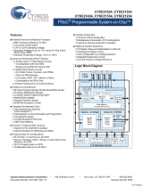
Internal
12 MHz
Oscillator
Clock
Control
Crystal
Oscillator
CY7C601xx only
POR /
Low-Voltage
Detect
Watchdog
Timer
M8C CPU
16 Extended
I/O Pins
16 GPIO
Pins
Wakeup
Timer
Capture
Timers
12-bit Timer
Vdd
Interrupt
Control
4 SPI/GPIO
Pins
Flash
8K Byte
RAM
256 Byte
2. Logic Block Diagram
[+] Feedback [+] Feedback

CY7C601xx, CY7C602xx
Document 38-16016 Rev. *E Page 2 of 68
3. Applications
The CY7C601xx and CY7C602xx are targeted for the following
applications:
■
PC wireless HID devices
❐
Mice (optomechanical, optical, trackball)
❐
Keyboards
❐
Presenter tools
■
Gaming
❐
Joysticks
❐
Gamepad
■
General purpose wireless applications
❐
Remote controls
❐
Barcode scanners
❐
POS terminal
❐
Consumer electronics
❐
Toys
4. Introduction
The enCoRe II LV family brings the features and benefits of the
enCoRe II to non USB applications. The enCoRe II family has an
integrated oscillator that eliminates the external crystal or
resonator, reducing overall cost. Other external components,
such as wakeup circuitry, are also integrated into this chip.
The enCoRe II LV is a low voltage, low cost 8-bit Flash program-
mable microcontroller.
The enCoRe II LV features up to 36 GPIO pins. The IO pins are
grouped into five ports (Port 0 to 4). The pins on Ports 0 and 1
are configured individually, when the pins on Ports 2, 3, and 4
are only configured as a group. Each GPIO port supports high
impedance inputs, configurable pull up, open drain output,
CMOS and TTL inputs, and CMOS output with up to five pins that
support programmable drive strength of up to 50 mA sink current.
Additionally, each IO pin is used to generate a GPIO interrupt to
the microcontroller. Each GPIO port has its own GPIO interrupt
vector with the exception of GPIO Port 0. GPIO Port 0 has, in
addition to the port interrupt vector, three dedicated pins that
have independent interrupt vectors (P0.2–P0.4).
The enCoRe II LV features an internal oscillator. Optionally, an
external 1 MHz to 24 MHz crystal is used to provide a higher
precision reference. The enCoRe II LV also supports external
clock.
The enCoRe II LV has 8 Kbytes of Flash for user code and 256
bytes of RAM for stack space and user variables.
In addition, enCoRe II LV includes a watchdog timer, a vectored
interrupt controller, a 16-bit free running timer with capture
registers, and a 12-bit programmable interval timer. The power
on reset circuit detects when power is applied to the device,
resets the logic to a known state, and executes instructions at
Flash address 0x0000. When power falls below a programmable
trip voltage, it generates a reset or is configured to generate an
interrupt. There is a low voltage detect circuit that detects when
V
CC
drops below a programmable trip voltage. This is config-
urable to generate a LVD interrupt to inform the processor about
the low voltage event. POR and LVD share the same interrupt;
there is no separate interrupt for each. The watchdog timer
ensures the firmware never gets stalled in an infinite loop.
The microcontroller supports 17 maskable interrupts in the
vectored interrupt controller. All interrupts can be masked.
Interrupt sources include LVR or POR, a programmable interval
timer, a nominal 1.024 ms programmable output from the free
running timer, two capture timers, five GPIO ports, three GPIO
pins, two SPI, a 16-bit free running timer wrap, and an internal
wakeup timer interrupt. The wakeup timer causes periodic inter-
rupts when enabled. The capture timers interrupt whenever a
new timer value is saved due to a selected GPIO edge event. A
total of eight GPIO interrupts support both TTL or CMOS
thresholds. For additional flexibility, on the edge-sensitive GPIO
pins, the interrupt polarity is programmable to be either rising or
falling.
The free running timer generates an interrupt at 1024 μs rate. It
also generates an interrupt when the free running counter
overflow occurs—every 16.384 ms. The duration of an event
under firmware control is measured by reading the timer at the
start and end of an event, then calculating the difference
between the two values. The two 8-bit capture timer registers
save a programmable 8-bit range of the free running timer when
a GPIO edge occurs on the two capture pins (P0.5 and P0.6).
The two 8-bit capture registers are ganged into a single 16-bit
capture register.
The enCoRe II LV supports in-system programming by using the
P1.0 and P1.1 pins as the serial programming mode interface.
5. Conventions
In this document, bit positions in the registers are shaded to
indicate which members of the enCoRe II LV family implement
the bits.
Available in all enCoRe II LV family members
CY7C601xx only
[+] Feedback [+] Feedback

CY7C601xx, CY7C602xx
Document 38-16016 Rev. *E Page 3 of 68
6. Pinouts
Figure 6-1. Package Configurations
1
2
3
4
5
6
9
11
15
16
17
18
19
20
22
21
NC
P0.7
TIO1/P0.6
TIO0/P0.5
INT2/P0.4
INT1/P0.3
CLKIN\P0.0
P2.0
P1.5/SMOSI
P1.3/SSEL
P3.1
P3.0
V
DD
P1.2
P1.1
P1.0
14
P1.4/SCLK
10
P2.1
NC
V
SS
12
13
7
8
INT0/P0.2
CLKOUT\P0.1
24
23
P1.7
P1.6/SMISO
24-Pin QSOP
CY7C60223
Top View
1
2
3
4
5
6
9
11
15
16
17
18
19
20
22
21
P3.0
P3.1
SCLK/P1.4
SMOSI/P1.5
SMISO/P1.6
P1.7
P0.7
TIO0/P0.5
V
DD
P2.0
P1.0
V
SS
P0.0/CLKIN
P2.1
P0.1/CLKOUT
P0.2/INT0
14
P1.1
10
TIO1/P0.6
INT2/P0.4
P0.3/INT1
12
13
7
8
NC
NC
24
23
P1.3/SSEL
P1.2
24-Pin PDIP
CY7C60223
1
2
3
4
5
6
9
11
15
16
17
18
19
20
22
21
NC
P0.7
TIO1/P0.6
TIO0/P0.5
INT2/P0.4
INT1/P0.3
CLKIN\P0.0
P2.0
P1.6/SMISO
P3.0
P1.4/SCLK
P3.1
P1.2
P1.3/SSEL
V
DD
P1.1
14
P1.5/SMOSI
10
P2.1
V
SS
P1.0
12
13
7
8
INT0/P0.2
CLKOUT\P0.1
24
23
NC
P1.7
24-Pin SOIC
CY7C60223
1
2
3
4
5
6
9
11
19
20
21
22
23
24
26
25
V
DD
P2.7
P2.6
P2.5
P2.4
P0.7
INT2/P0.4
INT0/P0.2
P3.6
P1.6/SMISO
P3.4
P1.7
P1.4/SCLK
P1.5/SMOSI
P1.3/SSEL
P1.2
18
P3.5
10
INT1/P0.3
CLKOUT/P0.1
V
DD
12
17
7
8
TIO1/P0.6
TIO0/P0.5
28
27
V
SS
P3.7
28-Pin SSOP
CY7C60113
15
16
P1.1
P1.0
13
CLKIN/P0.0
14
V
SS
1
2
3
4
5
6
9
11
V
DD
P4.1
P2.6
P2.4
10
P2.5
P2.3
12
7
8
P4.0
P2.7
40-Pin PDIP
CY7C60123
13
14
15
16
17
18
P2.2
P2.1
P2.0
P0.7
T1O1/P0.6
TIO0/P0.5
INT0/P0.2
CLKIN/P0.0
CLKOUT/P0.1
V
SS
19
INT2/P0.4
INT1/P0.3
21
22
23
24
26
25
P3.0
P1.4/SCLK
P1.6/SMISO
P1.5/SMOSI
P1.2
P1.3/SSEL
V
DD
P1.1
P1.7
P1.0
28
27
P3.2
P3.1
31
32
33
34
35
36
38
37
P4.2
V
SS
P4.3
P3.6
P3.7
P3.5
P3.4
30
P3.3
29
40
39
20
1
2
3
4
5
6
9
11
NC
NC
NC
NC
V
DD
P4.1
P2.6
P2.4
10
P2.5
P2.3
12
7
8
P4.0
P2.7
48-Pin SSOP
CY7C60123
13
14
15
16
17
18
21
23
P2.2
P2.1
P2.0
P0.7
TIO1/P0.6
TIO0/PO.5
INT0/P0.2
CLKIN/P0.0
22
CLKOUT/P0.1
V
SS
24
19
20
INT2/P0.4
INT1/P0.3
27
28
29
30
31
32
34
33
P3.0
P1.4/SCLK
P1.6/SMISO
P1.5/SMOSI
P1.2
P1.3/SSEL
V
DD
P1.1
26
P1.7
P1.025
36
35
P3.2
P3.1
39
40
41
42
43
44
46
45
NC
P4.2
V
SS
P4.3
P3.6
P3.7
P3.5
P3.4
38
NC
P3.337
48
47
NC
NC
[+] Feedback [+] Feedback

CY7C601xx, CY7C602xx
Document 38-16016 Rev. *E Page 4 of 68
6.1 Pin Assignments
Table 6-1. Pin Assignments
48
SSOP
40
PDIP
28
SSOP
24
QSOP
24
SOIC
24
PDIP
Name Description
7 3 P4.0 GPIO Port 4—configured as a group (nibble)
62 P4.1
42 38 P4.2
43 39 P4.3
34 30 19 18 1 P3.0 GPIO Port 3—configured as a group (byte)
35 31 20 19 2 P3.1
36 32 P3.2
37 33 P3.3
38 34 24 P3.4
39 35 25 P3.5
40 36 26 P3.6
41 37 27 P3.7
15 11 11 11 18 P2.0 GPIO Port 2—configured as a group (byte)
14 10 10 10 17 P2.1
13 9 P2.2
12 8 P2.3
11 7 5 P2.4
10 6 4 P2.5
953 P2.6
842 P2.7
25 21 15 14 13 20 P1.0 GPIO Port 1 bit 0
If this pin is used as a general purpose output it draws current.
It is, therefore, configured as an input to reduce current draw.
26 22 16 15 14 21 P1.1 GPIO Port 1 bit 1
If this pin is used as a general purpose output it draws current.
It is, therefore, configured as an input to reduce current draw.
28 24 18 17 16 23 P1.2 GPIO Port 1 bit 2
29 25 19 18 17 24 P1.3/SSEL GPIO Port 1 bit 3—Configured individually
Alternate function is SSEL signal of the SPI bus.
30 26 20 21 20 3 P1.4/SCLK GPIO Port 1 bit 4—Configured individually
Alternate function is SCLK signal of the SPI bus.
31 27 21 22 21 4 P1.5/SMOSI GPIO Port 1 bit 5—Configured individually
Alternate function is SMOSI signal of the SPI bus.
32 28 22 23 22 5 P1.6/SMISO GPIO Port 1 bit 6—Configured individually
Alternate function is SMISO signal of the SPI bus.
33 29 23 24 23 6 P1.7 GPIO Port 1 bit 7—Configured individually
TTL voltage threshold.
[+] Feedback [+] Feedback

CY7C601xx, CY7C602xx
Document 38-16016 Rev. *E Page 5 of 68
23 19 13 9 9 16 P0.0/CLKIN GPIO Port 0 bit 0—Configured individually
On CY7C601xx, optional Clock In when external oscillator is
disabled or external oscillator input when external oscillator is
enabled.
On CY7C602xx, oscillator input when configured as Clock In.
22 18 12 8 8 15 P0.1/CLKOUT GPIO Port 0 bit 1—Configured individually
On CY7C601xx, optional Clock Out when external oscillator is
disabled or external oscillator output drive when external oscil-
lator is enabled.
On CY7C602xx, oscillator output when configured as Clock Out.
21 17 11 7 7 14 P0.2/INT0 GPIO port 0 bit 2—Configured individually
Optional rising edge interrupt INT0.
20 16 10 6 6 13 P0.3/INT1 GPIO port 0 bit 3—Configured individually
Optional rising edge interrupt INT1.
19 15 9 5 5 12 P0.4/INT2 GPIO port 0 bit 4—Configured individually
Optional rising edge interrupt INT2.
18 14 8 4 4 11 P0.5/TIO0 GPIO port 0 bit 5—Configured individually
Alternate function timer capture inputs or timer output TIO0.
17 13 7 3 3 10 P0.6/TIO1 GPIO port 0 bit 6—Configured individually
Alternate function timer capture inputs or timer output TIO1.
16 12 6 2 2 9 P0.7 GPIO port 0 bit 7—Configured individually
1,2,3,
4
1 1 7 NC No connect
45,46,
47,48
12 24 8 NC No connect
5117 V
DD
Power
27 23 1 16 15 22
44 40 14 – – – V
SS
Ground
24 20 28 13 12 19
Table 6-1. Pin Assignments (continued)
48
SSOP
40
PDIP
28
SSOP
24
QSOP
24
SOIC
24
PDIP
Name Description
[+] Feedback [+] Feedback

CY7C601xx, CY7C602xx
Document 38-16016 Rev. *E Page 6 of 68
7. Register Summary
Table 7-1. enCoRe II LV Register Summary
The XIO bit in the CPU Flags Register must be set to access the extended register space for all registers above 0xFF.
Addr Name 7 6 5 4 3 2 1 0 R/W Default
00 P0DATA P0.7 P0.6/TIO1 P0.5/TIO0 P0.4/INT2 P0.3/INT1 P0.2/INT0 P0.1/
CLKOUT
P0.0/CLKIN bbbbbbbb 00000000
01 P1DATA P1.7 P1.6/SMISO P1.5/SMOSI P1.4/SCLK P1.3/SSEL P1.2 P1.1 P1.0 bbbbbbbb 00000000
02 P2DATA
P2.7–P2.2 P2.1–P2.0 bbbbbbbb 00000000
03 P3DATA
P3.7–P3.2 P3.1–P3.0 bbbbbbbb 00000000
04 P4DATA Reserved
P4.3–P4.0 ----bbbb 00000000
05 P00CR Reserved Int Enable Int Act Low TTL Thresh
High Sink Open Drain Pull up
Enable
Output
Enable
-bbbbbbb 00000000
06 P01CR CLK Output Int Enable Int Act Low TTL Thresh
High Sink Open Drain Pull Up
Enable
Output
Enable
bbbbbbbb 00000000
07–09 P02CR–
P04CR
Reserved Int Act Low TTL Thresh Reserved Open Drain Pull Up
Enable
Output
Enable
--bb-bbb 00000000
0A–0B P05CR–
P06CR
TIO Output Int Enable Int Act Low TTL Thresh Reserved Open Drain Pull Up
Enable
Output
Enable
bbbb-bbb 00000000
0C P07CR Reserved Int Enable Int Act Low TTL Thresh Reserved Open Drain Pull Up
Enable
Output
Enable
-bbb-bbb 00000000
0D P10CR Reserved Int Enable Int Act Low Reserved Output
Enable
-bb----b 00000000
0E P11CR Reserved Int Enable Int Act Low Reserved Open Drain Reserved Output
Enable
-bb--b-b 00000000
0F P12CR CLK Output Int Enable Int Act Low TTL
Threshold
Reserved Open Drain Pull Up
Enable
Output
Enable
bbbb-bbb 00000000
10 P13CR Reserved Int Enable Int Act Low Reserved High Sink Open Drain Pull Up
Enable
Output
Enable
-bb-bbbb 00000000
11–13 P14CR–
P16CR
SPI Use Int Enable Int Act Low Reserved High Sink Open Drain Pull Up
Enable
Output
Enable
bbb-bbbb 00000000
14 P17CR Reserved Int Enable Int Act Low Reserved High Sink Open Drain Pull Up
Enable
Output
Enable
-bb-bbbb 00000000
15 P2CR Reserved Int Enable Int Act Low TTL Thresh
High Sink Open Drain Pull Up
Enable
Output
Enable
-bbbbbbb 00000000
16 P3CR Reserved Int Enable Int Act Low TTL Thresh
High Sink Open Drain Pull Up
Enable
Output
Enable
-bbbbbbb 00000000
17 P4CR
Reserved Int Enable Int Act Low TTL Thresh Reserved Open Drain Pull Up
Enable
Output
Enable
-bbb-bbb 00000000
20 FRTMRL Free Running Timer [7:0] bbbbbbbb 00000000
21 FRTMRH Free Running Timer [15:8] bbbbbbbb 00000000
22 TCAP0R Capture 0 Rising [7:0] rrrrrrrr 00000000
23 TCAP1R Capture 1 Rising [7:0] rrrrrrrr 00000000
24 TCAP0F Capture 0 Falling [7:0] rrrrrrrr 00000000
25 TCAP1F Capture 1 Falling [7:0] rrrrrrrr 00000000
26 PITMRL Prog Interval Timer [7:0] rrrrrrrr 00000000
27 PITMRH Reserved Prog Interval Timer [11:8] ----rrrr 00000000
28 PIRL Prog Interval [7:0] bbbbbbbb 00000000
29 PIRH Reserved Prog Interval [11:8] ----bbbb 00000000
2A TMRCR First Edge
Hold
8-bit Capture Prescale Cap0 16-bit
Enable
Reserved bbbbb--- 00000000
2B TCAPINTE Reserved Cap1 Fall
Active
Cap1 Rise
Active
Cap0 Fall
Active
Cap0 Rise
Active
----bbbb 00000000
2C TCAPINTS Reserved Cap1 Fall
Active
Cap1 Rise
Active
Cap0 Fall
Active
Cap0 Rise
Active
----bbbb 00000000
30 CPUCLKCR Reserved CPU
CLK Select
-------b 00000000
31 TMRCLKCR TCAPCLK Divider TCAPCLK Select ITMRCLK Divider ITMRCLK Select bbbbbbbb 10001111
32 CLKIOCR Reserved
XOSC
Select
XOSC
Enable
EFTB
Disabled
CLKOUT Select ---bbbbb 00000000
[+] Feedback [+] Feedback

CY7C601xx, CY7C602xx
Document 38-16016 Rev. *E Page 7 of 68
Note In the R/W column:
b = Both Read and Write
r = Read Only
w = Write Only
c = Read or Clear
d = Calibration Value. Must not change during normal use
34 IOSCTR foffset[2:0] Gain[4:0] bbbbbbbb 000ddddd
35 XOSCTR Reserved
XOSC XGM [2:0] Reserved Mode ---bbb-b 000ddddd
36 LPOSCTR 32 kHz Low
Power
Reserved 32 kHz Bias Trim [1:0] 32 kHz Freq Trim [3:0] b-bbbbbb d-dddddd
3C SPIDATA SPIData[7:0] bbbbbbbb 00000000
3D SPICR Swap LSB First Comm Mode CPOL CPHA SCLK Select bbbbbbbb 00000000
DA INT_CLR0 GPIO Port 1 Sleep Timer INT1 GPIO Port 0 SPI Receive SPI Transmit INT0 POR/LVD bbbbbbbb 00000000
DB INT_CLR1 TCAP0 Prog Interval
Timer
1 ms Timer Reserved bbb----- 00000000
DC INT_CLR2 Reserved GPIO Port 4 GPIO Port 3 GPIO Port 2 Reserved INT2 16-bit
Counter
Wrap
TCAP1 -bbb-bbb 00000000
DE INT_MSK3 ENSWINT Reserved r------- 00000000
DF INT_MSK2 Reserved GPIO Port 4
Int Enable
GPIO Port 3
Int Enable
GPIO Port 2
Int Enable
Reserved INT2
Int Enable
16-bit
Counter
Wrap Int
Enable
TCAP1
Int Enable
-bbb-bbb 00000000
E1 INT_MSK1 TCAP0
Int Enable
Prog Interval
Timer
Int Enable
1 ms Timer
Int Enable
Reserved bbb----- 00000000
E0 INT_MSK0 GPIO Port 1
Int Enable
Sleep Timer
Int Enable
INT1
Int Enable
GPIO Port 0
Int Enable
SPI Receive
Int Enable
SPI Transmit
Int Enable
INT0
Int Enable
POR/LVD
Int Enable
bbbbbbbb 00000000
E2 INT_VC Pending Interrupt [7:0] bbbbbbbb 00000000
E3 RESWDT Reset Watchdog Timer [7:0] wwwwwww
w
00000000
-- CPU_A Temporary Register T1 [7:0] -------- 00000000
-- CPU_X X[7:0] -------- 00000000
-- CPU_PCL Program Counter [7:0] -------- 00000000
-- CPU_PCH Program Counter [15:8] -------- 00000000
-- CPU_SP Stack Pointer [7:0] -------- 00000000
F7 CPU_F Reserved XIO Super Carry Zero Global IE ---brbbb 00000010
FF CPU_SCR GIES Reserved WDRS PORS Sleep Reserved Reserved Stop r-ccb--b 00010100
1E0 OSC_CR0 Reserved No Buzz Sleep Timer [1:0] CPU Speed [2:0] --bbbbbb 00000000
1E3 LVDCR Reserved PORLEV[1:0] Reserved VM[2:0] --bb-bbb 00000000
1EB ECO_TR Sleep Duty Cycle [1:0] Reserved bb------ 00000000
1E4 VLTCMP Reserved LVD PPOR ------rr 00000000
Table 7-1. enCoRe II LV Register Summary (continued)
The XIO bit in the CPU Flags Register must be set to access the extended register space for all registers above 0xFF.
Addr Name 7 6 5 4 3 2 1 0 R/W Default
[+] Feedback [+] Feedback

CY7C601xx, CY7C602xx
Document 38-16016 Rev. *E Page 8 of 68
8. CPU Architecture
This family of microcontrollers is based on a high performance,
8-bit, Harvard architecture microprocessor. Five registers control
the primary operation of the CPU core. These registers are
affected by various instructions, but are not directly accessible
through the register space by the user.
The 16-bit Program Counter Register (CPU_PC) directly
addresses the full 8 Kbytes of program memory space.
The Accumulator Register (CPU_A) is the general purpose
register that holds results of instructions that specify any of the
source addressing modes.
The Index Register (CPU_X) holds an offset value used in the
indexed addressing modes. Typically, this is used to address a
block of data within the data memory space.
The Stack Pointer Register (CPU_SP) holds the address of the
current top-of-stack in the data memory space. It is affected by
the PUSH, POP, LCALL, CALL, RETI, and RET instructions,
which manage the software stack. It is also affected by the SWAP
and ADD instructions.
The Flag Register (CPU_F) has three status bits: Zero Flag bit
[1]; Carry Flag bit [2]; Supervisory State bit [3]. The Global
Interrupt Enable bit [0] is used to globally enable or disable inter-
rupts. The user cannot manipulate the Supervisory State status
bit [3]. The flags are affected by arithmetic, logic, and shift opera-
tions. The manner in which each flag is changed is dependent
upon the instruction being executed (AND, OR, XOR). See
Table 10 -1.
9. CPU Registers
9.1 Flags Register
The Flags Register is only set or reset with logical instruction.
Table 8-1. CPU Registers and Register Name
Register Register Name
Flags CPU_F
Program Counter CPU_PC
Accumulator CPU_A
Stack Pointer CPU_SP
Index CPU_X
Table 9-1. CPU Flags Register (CPU_F) [R/W]
Bit # 7 6 5 4 3 2 1 0
Field Reserved XIO Super Carry Zero Global IE
Read/Write – – – R/W R R/W R/W R/W
Default 00000010
Bit [7:5]: Reserved
Bit 4: XIO
Set by the user to select between the register banks.
0 = Bank 0
1 = Bank 1
Bit 3: Super
Indicates whether the CPU is executing user code or supervisor code. (This code cannot be accessed directly by the user.)
0 = User Code
1 = Supervisor Code
Bit 2: Carry
Set by CPU to indicate whether there is a carry in the previous logical or arithmetic operation.
0 = No Carry
1 = Carry
Bit 1: Zero
Set by CPU to indicate whether there is a zero result in the previous logical or arithmetic operation.
0 = Not Equal to Zero
1 = Equal to Zero
Bit 0: Global IE
Determines whether all interrupts are enabled or disabled.
0 = Disabled
1 = Enabled
Note This register is readable with explicit address 0xF7. The OR F, expr and AND F, expr are used to set and clear the CPU_F
bits.
[+] Feedback [+] Feedback

CY7C601xx, CY7C602xx
Document 38-16016 Rev. *E Page 9 of 68
9.1.1 Accumulator Register
9.1.2 Index Register
9.1.3 Stack Pointer Register
9.1.4 CPU Program Counter High Register
9.1.5 CPU Program Counter Low Register
Table 9-2. CPU Accumulator Register (CPU_A)
Bit # 7 6 5 4 3 2 1 0
Field CPU Accumulator [7:0]
Read/Write ––––––––
Default 00000000
Bit [7:0]: CPU Accumulator [7:0]
8-bit data value holds the result of any logical or arithmetic instruction that uses a source addressing mode.
Table 9-3. CPU X Register (CPU_X)
Bit # 7 6 5 4 3 2 1 0
Field X [7:0]
Read/Write ––––––––
Default 00000000
Bit [7:0]: X [7:0]
8-bit data value holds an index for any instruction that uses an indexed addressing mode.
Table 9-4. CPU Stack Pointer Register (CPU_SP)
Bit # 7 6 5 4 3 2 1 0
Field Stack Pointer [7:0]
Read/Write ––––––––
Default 00000000
Bit [7:0]: Stack Pointer [7:0]
8-bit data value holds a pointer to the current top-of-stack.
Table 9-5. CPU Program Counter High Register (CPU_PCH)
Bit # 7 6 5 4 3 2 1 0
Field Program Counter [15:8]
Read/Write ––––––––
Default 00000000
Bit [7:0]: Program Counter [15:8]
8-bit data value holds the higher byte of the program counter.
Table 9-6. CPU Program Counter Low Register (CPU_PCL)
Bit # 7 6 5 4 3 2 1 0
Field Program Counter [7:0]
Read/Write ––––––––
Default 00000000
Bit [7:0]: Program Counter [7:0]
8-bit data value holds the lower byte of the program counter.
[+] Feedback [+] Feedback

CY7C601xx, CY7C602xx
Document 38-16016 Rev. *E Page 10 of 68
9.2 Addressing Modes
9.2.1 Source Immediate
The result of an instruction using this addressing mode is placed
in the A register, the F register, the SP register, or the X register,
which is specified as part of the instruction opcode. Operand 1
is an immediate value that serves as a source for the instruction.
Arithmetic instructions require two sources; the second source is
the A, X, SP, or F register specified in the opcode. Instructions
using this addressing mode are two bytes in length.
Examples
9.2.2 Source Direct
The result of an instruction using this addressing mode is placed
in either the A register or the X register, which is specified as part
of the instruction opcode. Operand 1 is an address that points to
a location in either the RAM memory space or the register space
that is the source for the instruction. Arithmetic instructions
require two sources; the second source is the A register or X
register specified in the opcode. Instructions using this
addressing mode are two bytes in length.
Examples
9.2.3 Source Indexed
The result of an instruction using this addressing mode is placed
in either the A register or the X register, which is specified as part
of the instruction opcode. Operand 1 is added to the X register
forming an address that points to a location in either the RAM
memory space or the register space that is the source for the
instruction. Arithmetic instructions require two sources; the
second source is the A register or X register specified in the
opcode. Instructions using this addressing mode are two bytes
in length.
Examples
9.2.4 Destination Direct
The result of an instruction using this addressing mode is placed
within either the RAM memory space or the register space.
Operand 1 is an address that points to the location of the result.
The source for the instruction is either the A register or the X
register, which is specified as part of the instruction opcode.
Arithmetic instructions require two sources; the second source is
the location specified by Operand 1. Instructions using this
addressing mode are two bytes in length.
Examples
Table 9-7. Source Immediate
Opcode Operand 1
Instruction Immediate Value
ADD A, 7 ;In this case, the immediate value of 7 is added
with the Accumulator and the result is placed in
the Accumulator.
MOV X, 8 ;In this case, the immediate value of 8 is moved
to the X register.
AND F, 9 ;In this case, the immediate value of 9 is logically
ANDed with the F register and the result is placed
in the F register.
Table 9-8. Source Direct
Opcode Operand 1
Instruction Source Address
ADD A, [7] ;In this case, the value in the RAM
memory location at address 7 is added
with the Accumulator, and the result is
placed in the Accumulator.
MOV X, REG[8] ;In this case, the value in the register
space at address 8 is moved to the X
register.
Table 9-9. Source Indexed
Opcode Operand 1
Instruction Source Index
ADD A, [X+7] ;In this case, the value in the memory
location at address X + 7 is added with
the Accumulator, and the result is
placed in the Accumulator.
MOV X, REG[X+8] ;In this case, the value in the register
space at address X + 8 is moved to the
X register.
Table 9-10. Destination Direct
Opcode Operand 1
Instruction Destination Address
ADD [7], A ;In this case, the value in the memory
location at address 7 is added with the
Accumulator, and the result is placed
in the memory location at address 7.
The Accumulator is unchanged.
MOV REG[8], A ;In this case, the Accumulator is
moved to the register space location at
address 8. The Accumulator is
unchanged.
[+] Feedback [+] Feedback

CY7C601xx, CY7C602xx
Document 38-16016 Rev. *E Page 11 of 68
9.2.5 Destination Indexed
The result of an instruction using this addressing mode is placed
within either the RAM memory space or the register space.
Operand 1 is added to the X register forming the address that
points to the location of the result. The source for the instruction
is the A register. Arithmetic instructions require two sources; the
second source is the location specified by Operand 1 added with
the X register. Instructions using this addressing mode are two
bytes in length.
Example
9.2.6 Destination Direct Source Immediate
The result of an instruction using this addressing mode is placed
within either the RAM memory space or the register space.
Operand 1 is the address of the result. The source for the
instruction is Operand 2, which is an immediate value. Arithmetic
instructions require two sources; the second source is the
location specified by Operand 1. Instructions using this
addressing mode are three bytes in length.
Examples
9.2.7 Destination Indexed Source Immediate
The result of an instruction using this addressing mode is placed
within either the RAM memory space or the register space.
Operand 1 is added to the X register to form the address of the
result. The source for the instruction is Operand 2, which is an
immediate value. Arithmetic instructions require two sources; the
second source is the location specified by Operand 1 added with
the X register. Instructions using this addressing mode are three
bytes in length.
Examples
9.2.8 Destination Direct Source Direct
The result of an instruction using this addressing mode is placed
within the RAM memory. Operand 1 is the address of the result.
Operand 2 is an address that points to a location in the RAM
memory that is the source for the instruction. This addressing
mode is only valid on the MOV instruction. The instruction using
this addressing mode is three bytes in length.
Example
Table 9-11. Destination Indexed
Opcode Operand 1
Instruction Destination Index
ADD [X+7], A ;In this case, the value in the memory
location at address X+7 is added with the
Accumulator and the result is placed in the
memory location at address X+7. The
Accumulator is unchanged.
Table 9-12. Destination Direct Source Immediate
Opcode Operand 1 Operand 2
Instruction Destination Address Immediate Value
ADD [7], 5 ;In this case, value in the memory location
at address 7 is added to the immediate
value of 5, and the result is placed in the
memory location at address 7.
MOV REG[8], 6 ;In this case, the immediate value of 6 is
moved into the register space location at
address 8.
Table 9-13. Destination Indexed Source Immediate
Opcode Operand 1 Operand 2
Instruction Destination Index Immediate Value
ADD [X+7], 5 ;In this case, the value in the memory
location at address X+7 is added
with the immediate value of 5, and
the result is placed in the memory
location at address X+7.
MOV REG[X+8], 6 ;In this case, the immediate value of
6 is moved into the location in the
register space at address X+8.
Table 9-14. Destination Direct Source Direct
Opcode Operand 1 Operand 2
Instruction Destination Address Source Address
MOV [7], [8] ;In this case, the value in the memory location
at address 8 is moved to the memory location
at address 7.
[+] Feedback [+] Feedback

CY7C601xx, CY7C602xx
Document 38-16016 Rev. *E Page 12 of 68
9.2.9 Source Indirect Post Increment
The result of an instruction using this addressing mode is placed
in the Accumulator. Operand 1 is an address pointing to a
location within the memory space, which contains an address
(the indirect address) for the source of the instruction. The
indirect address is incremented as part of the instruction
execution. This addressing mode is only valid on the MVI
instruction. The instruction using this addressing mode is two
bytes in length. Refer to the PSoC Designer: Assembly
Language User Guide for further details on MVI instruction.
Example
9.2.10 Destination Indirect Post Increment
The result of an instruction using this addressing mode is placed
within the memory space. Operand 1 is an address pointing to a
location within the memory space, which contains an address
(the indirect address) for the destination of the instruction. The
indirect address is incremented as part of the instruction
execution. The source for the instruction is the Accumulator. This
addressing mode is only valid on the MVI instruction. The
instruction using this addressing mode is two bytes in length.
Example
10. Instruction Set Summary
The instruction set is summarized in Table 10-1 numerically and serves as a quick reference. For more information, the Instruction
Set Summary tables are described in detail in the PSoC Designer Assembly Language User Guide (available on the www.cypress.com
web site).
Table 9-15. Source Indirect Post Increment
Opcode Operand 1
Instruction Source Address Address
MVI A, [8] ;In this case, the value in the memory location
at address 8 is an indirect address. The
memory location pointed to by the Indirect
address is moved into the Accumulator. The
indirect address is then incremented.
Table 9-16. Destination Indirect Post Increment
Opcode Operand 1
Instruction Destination Address Address
MVI [8], A ;In this case, the value in the memory
location at address 8 is an
indirect;address. The Accumulator is
moved into the memory location pointed
to by the indirect address. The indirect
address is then incremented.
Table 10-1. Instruction Set Summary Sorted Numerically by Opcode Order
Opcode Hex
Cycles
Bytes
Instruction Format
[1, 2]
Flags
Opcode Hex
Cycles
Bytes
Instruction Format Flags
Opcode Hex
Cycles
Bytes
Instruction Format Flags
00 15 1 SSC 2D 8 2 OR [X+expr], A Z 5A 5 2 MOV [expr], X
01 4 2 ADD A, expr C, Z 2E 9 3 OR [expr], expr Z 5B 4 1 MOV A, X Z
02 6 2 ADD A, [expr] C, Z 2F 10 3 OR [X+expr], expr Z 5C 4 1 MOV X, A
03 7 2 ADD A, [X+expr] C, Z 30 9 1 HALT 5D 6 2 MOV A, reg[expr] Z
04 7 2 ADD [expr], A C, Z 31 4 2 XOR A, expr Z 5E 7 2 MOV A, reg[X+expr] Z
05 8 2 ADD [X+expr], A C, Z 32 6 2 XOR A, [expr] Z 5F 10 3 MOV [expr], [expr]
06 9 3 ADD [expr], expr C, Z 33 7 2 XOR A, [X+expr] Z 60 5 2 MOV reg[expr], A
07 10 3 ADD [X+expr], expr C, Z 34 7 2 XOR [expr], A Z 61 6 2 MOV reg[X+expr], A
08 4 1 PUSH A 35 8 2 XOR [X+expr], A Z 62 8 3 MOV reg[expr], expr
09 4 2 ADC A, expr C, Z 36 9 3 XOR [expr], expr Z 63 9 3 MOV reg[X+expr],
expr
0A 6 2 ADC A, [expr] C, Z 37 10 3 XOR [X+expr], expr Z 64 4 1 ASL A C, Z
0B 7 2 ADC A, [X+expr] C, Z 38 5 2 ADD SP, expr 65 7 2 ASL [expr] C, Z
0C 7 2 ADC [expr], A C, Z 39 5 2 CMP A, expr if (A=B)
Z=1
if (A<B)
C=1
66 8 2 ASL [X+expr] C, Z
0D 8 2 ADC [X+expr], A C, Z 3A 7 2 CMP A, [expr] 67 4 1 ASR A C, Z
0E 9 3 ADC [expr], expr C, Z 3B 8 2 CMP A, [X+expr] 68 7 2 ASR [expr] C, Z
0F 10 3 ADC [X+expr], expr C, Z 3C 8 3 CMP [expr], expr 69 8 2 ASR [X+expr] C, Z
10 4 1 PUSH X 3D 9 3 CMP [X+expr], expr 6A 4 1 RLC A C, Z
11 4 2 SUB A, expr C, Z 3E 10 2 MVI A, [ [expr]++ ] Z 6B 7 2 RLC [expr] C, Z
12 6 2 SUB A, [expr] C, Z 3F 10 2 MVI [ [expr]++ ], A 6C 8 2 RLC [X+expr] C, Z
[+] Feedback [+] Feedback

CY7C601xx, CY7C602xx
Document 38-16016 Rev. *E Page 13 of 68
13 7 2 SUB A, [X+expr] C, Z 40 4 1 NOP 6D 4 1 RRC A C, Z
14 7 2 SUB [expr], A C, Z 41 9 3 AND reg[expr], expr Z 6E 7 2 RRC [expr] C, Z
15 8 2 SUB [X+expr], A C, Z 42 10 3 AND reg[X+expr],
expr
Z 6F 8 2 RRC [X+expr] C, Z
16 9 3 SUB [expr], expr C, Z 43 9 3 OR reg[expr], expr Z 70 4 2 AND F, expr C, Z
17 10 3 SUB [X+expr], expr C, Z 44 10 3 OR reg[X+expr], expr Z 71 4 2 OR F, expr C, Z
18 5 1 POP A Z 45 9 3 XOR reg[expr], expr Z 72 4 2 XOR F, expr C, Z
19 4 2 SBB A, expr C, Z 46 10 3 XOR reg[X+expr],
expr
Z 73 4 1 CPL A Z
1A 6 2 SBB A, [expr] C, Z 47 8 3 TST [expr], expr Z 74 4 1 INC A C, Z
1B 7 2 SBB A, [X+expr] C, Z 48 9 3 TST [X+expr], expr Z 75 4 1 INC X C, Z
1C 7 2 SBB [expr], A C, Z 49 9 3 TST reg[expr], expr Z 76 7 2 INC [expr] C, Z
1D 8 2 SBB [X+expr], A C, Z 4A 10 3 TST reg[X+expr], expr Z 77 8 2 INC [X+expr] C, Z
1E 9 3 SBB [expr], expr C, Z 4B 5 1 SWAP A, X Z 78 4 1 DEC A C, Z
1F 10 3 SBB [X+expr], expr C, Z 4C 7 2 SWAP A, [expr] Z 79 4 1 DEC X C, Z
20 5 1 POP X 4D 7 2 SWAP X, [expr] 7A 7 2 DEC [expr] C, Z
21 4 2 AND A, expr Z 4E 5 1 SWAP A, SP Z 7B 8 2 DEC [X+expr] C, Z
22 6 2 AND A, [expr] Z 4F 4 1 MOV X, SP 7C 13 3 LCALL
23 7 2 AND A, [X+expr] Z 50 4 2 MOV A, expr Z 7D 7 3 LJMP
24 7 2 AND [expr], A Z 51 5 2 MOV A, [expr] Z 7E 10 1 RETI C, Z
25 8 2 AND [X+expr], A Z 52 6 2 MOV A, [X+expr] Z 7F 8 1 RET
26 9 3 AND [expr], expr Z 53 5 2 MOV [expr], A 8x 5 2 JMP
27 10 3 AND [X+expr], expr Z 54 6 2 MOV [X+expr], A 9x 11 2 CALL
28 11 1 ROMX Z 55 8 3 MOV [expr], expr Ax 5 2 JZ
29 4 2 OR A, expr Z 56 9 3 MOV [X+expr], expr Bx 5 2 JNZ
2A 6 2 OR A, [expr] Z 57 4 2 MOV X, expr Cx 5 2 JC
2B 7 2 OR A, [X+expr] Z 58 6 2 MOV X, [expr] Dx 5 2 JNC
2C 7 2 OR [expr], A Z 59 7 2 MOV X, [X+expr] Ex 7 2 JACC
Fx 13 2 INDEX Z
Table 10-1. Instruction Set Summary Sorted Numerically by Opcode Order (continued)
Opcode Hex
Cycles
Bytes
Instruction Format
[1, 2]
Flags
Opcode Hex
Cycles
Bytes
Instruction Format Flags
Opcode Hex
Cycles
Bytes
Instruction Format Flags
Notes
1. Interrupt routines take 13 cycles before execution resumes at interrupt vector table.
2. The number of cycles required by an instruction is increased by one for instructions that span 256 byte boundaries in the Flash memory space.
[+] Feedback [+] Feedback

CY7C601xx, CY7C602xx
Document 38-16016 Rev. *E Page 14 of 68
11. Memory Organization
11.1 Flash Program Memory Organization
Figure 11-1. Program Memory Space with Interrupt Vector Table
after reset Address
16-bit PC 0x0000 Program execution begins here after a reset
0x0004 POR/LVD
0x0008 INT0
0x000C SPI Transmitter Empty
0x0010 SPI Receiver Full
0x0014 GPIO Port 0
0x0018 GPIO Port 1
0x001C INT1
0x0020 Reserved
0x0024 Reserved
0x0028 Reserved
0x002C Reserved
0x0030 Reserved
0x0034 1 ms Interval timer
0x0038 Programmable Interval Timer
0x003C Timer Capture 0
0x0040 Timer Capture 1
0x0044 16-bit Free Running Timer Wrap
0x0048 INT2
0x004C Reserved
0x0050 GPIO Port 2
0x0054 GPIO Port 3
0x0058 GPIO Port 4
0x005C Reserved
0x0060 Reserved
0x0064 Sleep Timer
0x0068 Program Memory begins here (if below interrupts not used,
program memory can start lower)
0x1FFF
[+] Feedback [+] Feedback

CY7C601xx, CY7C602xx
Document 38-16016 Rev. *E Page 15 of 68
11.2 Data Memory Organization
The CY7C601xx and CY7C602xx microcontrollers provide up to 256 bytes of data RAM
Figure 11-2. Data Memory Organization
11.3 Flash
This section describes the Flash block of enCoRe II LV. Much of
the visible Flash functionality, including programming and
security, are implemented in the M8C Supervisory Read Only
Memory (SROM). enCoRe II LV Flash has an endurance of 1000
erase and write cycles and a ten year data retention capability.
11.3.1 Flash Programming and Security
All Flash programming is performed by code in the SROM. The
registers that control Flash programming are only visible to the
M8C CPU when it is executing out of SROM. This makes it
impossible to read, write, or erase the Flash by avoiding the
security mechanisms implemented in the SROM.
Customer firmware only programs Flash via SROM calls. The
data or code images are sourced through any interface with the
appropriate support firmware. This type of programming requires
a ‘boot-loader’—a piece of firmware resident on the Flash. For
safety reasons this boot-loader is not overwritten during firmware
rewrites.
The Flash provides four extra auxiliary rows to hold Flash block
protection flags, boot time calibration values, configuration
tables, and any device values. The routines to access these
auxiliary rows are documented in the SROM section. The
auxiliary rows are not affected by the device erase function.
11.3.2 In-System Programming
enCoRe II LV devices enable in-system programming by using
the P1.0 and P1.1 pins as the serial programming mode
interface. This allows an external controller to make the enCoRe
II LV part enter serial programming mode and then use the test
queue to issue Flash access functions in the SROM.
11.4 SROM
The SROM holds the code to boot the part, calibrate circuitry, and
perform Flash operations (Table 11-1 lists the SROM functions).
The functions of the SROM are accessed in normal user code or
operating from Flash. The SROM exists in a separate memory
space from user code. To access SROM functions, the Super-
visory System Call instruction (SSC) is executed, which has an
opcode of 00h. Before executing SSC, the M8C’s accumulator is
loaded with the desired SROM function code from Table 11-1.
Undefined functions causes a HALT if called from user code. The
SROM functions execute code with calls; therefore, the functions
require stack space. With the exception of Reset, all of the
SROM functions have a parameter block in SRAM that must be
configured before executing the SSC. Table 11-2 lists all possible
parameter block variables. The meaning of each parameter, with
regards to a specific SROM function, is described later in this
section.
After Reset Address
8-bit PSP 0x00 Stack begins here and grows upward
Top of RAM Memory 0xFF
Table 11-1. SROM Function Codes
Function Code Function Name Stack Space
00h SWBootReset 0
01h ReadBlock 7
02h WriteBlock 10
03h EraseBlock 9
05h EraseAll 11
06h TableRead 3
07h CheckSum 3
[+] Feedback [+] Feedback

CY7C601xx, CY7C602xx
Document 38-16016 Rev. *E Page 16 of 68
Two important variables used for all functions are KEY1 and
KEY2. These variables help discriminate between valid and
inadvertent SSCs. KEY1 always has a value of 3Ah, while KEY2
has the same value as the stack pointer when the SROM
function begins execution. This is the Stack Pointer value when
the SSC opcode is executed, plus three. If either of the keys do
not match the expected values, the M8C halts (with the exception
of the SWBootReset function). The following code puts the
correct value in KEY1 and KEY2. The code starts with a halt, to
force the program to jump directly into the setup code and not
run into it.
halt
SSCOP: mov [KEY1], 3ah
mov X, SP
mov A, X
add A, 3
mov [KEY2], A
11.4.1 Return Codes
The SROM also features Return Codes and Lockouts.
Return codes determine the success or failure of a particular
function. The return code is stored in KEY1’s position in the
parameter block. The CheckSum and TableRead functions do
not have return codes because KEY1’s position in the parameter
block is used to return other data.
Read, write, and erase operations may fail if the target block is
read or write protected. Block protection levels are set during
device programming.
The EraseAll function overwrites data in addition to leaving the
entire user Flash in the erase state. The EraseAll function loops
through the number of Flash macros in the product, executing
the following sequence: erase, bulk program all zeros, erase.
After the user space in all Flash macros are erased, a second
loop erases and then programs each protection block with zeros.
11.5 SROM Function Descriptions
11.5.1 SWBootReset Function
The SROM function, SWBootReset, is responsible for transi-
tioning the device from a reset state to running user code. The
SWBootReset function is executed whenever the SROM is
entered with an M8C accumulator value of 00h: the SRAM
parameter block is not used as an input to the function. This
happens, by design, after a hardware reset, because the M8C's
accumulator is reset to 00h or when user code executes the SSC
instruction with an accumulator value of 00h. The SWBootReset
function does not execute when the SSC instruction is executed
with a bad key value and a non zero function code. An enCoRe
II LV device executes the HALT instruction if a bad value is given
for either KEY1 or KEY2.
The SWBootReset function verifies the integrity of the calibration
data by way of a 16-bit checksum, before releasing the M8C to
run user code.
11.5.2 ReadBlock Function
The ReadBlock function is used to read 64 contiguous bytes
from Flash: a block.
The function first checks the protection bits and determines if the
desired BLOCKID is readable. If read protection is turned on, the
ReadBlock function exits setting the accumulator and KEY2 back
to 00h. KEY1 has a value of 01h, indicating a read failure. If read
protection is not enabled, the function reads 64 bytes from the
Flash using a ROMX instruction and stores the results in SRAM
using an MVI instruction. The first of the 64 bytes is stored in
SRAM at the address indicated by the value of the POINTER
parameter. When the ReadBlock completes successfully the
accumulator, KEY1 and KEY2 all have a value of 00h.
Table 11-2. SROM Function Parameters
Variable Name SRAM Address
Key1/Counter/Return Code 0,F8h
Key2/TMP 0,F9h
BlockID 0,FAh
Pointer 0,FBh
Clock 0,FCh
Mode 0,FDh
Delay 0,FEh
PCL 0,FFh
Table 11-3. SROM Return Codes
Return Code Description
00h Success
01h Function not allowed due to level of protection
on block
02h Software reset without hardware reset
03h Fatal error, SROM halted
Table 11-4. ReadBlock Parameters
Name Address Description
KEY1 0,F8h 3Ah
KEY2 0,F9h Stack Pointer value, when SSC is
executed
BLOCKID 0,FAh Flash block number
POINTER 0,FBh First of 64 addresses in SRAM
where returned data is stored
[+] Feedback [+] Feedback

CY7C601xx, CY7C602xx
Document 38-16016 Rev. *E Page 17 of 68
11.5.3 WriteBlock Function
The WriteBlock function is used to store data in Flash. Data is
moved 64 bytes at a time from SRAM to Flash using this function.
The WriteBlock function first checks the protection bits and deter-
mines if the desired BLOCKID is writable. If write protection is
turned on, the WriteBlock function exits setting the accumulator
and KEY2 back to 00h. KEY1 has a value of 01h, indicating a
write failure. The configuration of the WriteBlock function is
straightforward. The BLOCKID of the Flash block, where the
data is stored, is determined and stored at SRAM address FAh.
The SRAM address of the first of the 64 bytes to be stored in
Flash is indicated using the POINTER variable in the parameter
block (SRAM address FBh). Finally, the CLOCK and DELAY
value are set correctly. The CLOCK value determines the length
of the write pulse used to store the data in Flash. The CLOCK
and DELAY values are dependent on the CPU speed and must
be set correctly. Refer to the Clocking section for additional infor-
mation.
11.5.4 EraseBlock Function
The EraseBlock function is used to erase a block of 64
contiguous bytes in Flash. The EraseBlock function first checks
the protection bits and determines if the desired BLOCKID is
writable. If write protection is turned on, the EraseBlock function
exits setting the accumulator and KEY2 back to 00h. KEY1 has
a value of 01h, indicating a write failure. The EraseBlock function
is only useful as the first step in programming. Erasing a block
does not make data in a block fully unreadable. If the objective
is to obliterate data in a block, the best method is to perform an
EraseBlock followed by a WriteBlock of all zeros.
To set up the parameter block for EraseBlock, correct key values
must be stored in KEY1 and KEY2. The block number to be
erased is stored in the BLOCKID variable and the CLOCK and
DELAY values are set based on the current CPU speed.
11.5.5 ProtectBlock Function
The enCoRe II LV devices offer Flash protection on a
block-by-block basis. Table 11-7 lists the protection modes
available. In the table, ER and EW indicate the ability to perform
external reads and writes; IW is used for internal writes. Internal
reading is always permitted using the ROMX instruction. The
ability to read using the SROM ReadBlock function is indicated
by SR. The protection level is stored in two bits according to
Table 11-7. These bits are bit packed into 64 bytes of the
protection block. Therefore, each protection block byte stores
the protection level for four Flash blocks. The bits are packed into
a byte, with the lowest numbered block’s protection level stored
in the lowest numbered bits in Table 11-7.
The first address of the protection block contains the protection
level for blocks 0 through 3; the second address is for blocks 4
through 7. The 64th byte stores the protection level for blocks
252 through 255.
Only an EraseAll decreases the protection level by placing zeros
in all locations of the protection block. To set the level of
protection, the ProtectBlock function is used. This function takes
data from SRAM, starting at address 80h, and ORs it with the
current values in the protection block. The result of the OR
operation is then stored in the protection block. The EraseBlock
function does not change the protection level for a block.
Because the SRAM location for the protection data is fixed and
there is only one protection block per Flash macro, the Protect-
Block function expects very few variables in the parameter block
to be set before calling the function. The parameter block values
that are, besides the keys, are the CLOCK and DELAY values.
Table 11-5. WriteBlock Parameters
Name Address Description
KEY1 0,F8h 3Ah
KEY2 0,F9h Stack Pointer value, when SSC is
executing
BLOCK ID 0,FAh 8 KB Flash block number (00h–7Fh)
4 KB Flash block number (00h–3Fh)
3 KB Flash block number (00h–2Fh)
POINTER 0,FBh First 64 addresses in SRAM where
the data is stored in Flash is located
before calling WriteBlock
CLOCK 0,FCh Clock Divider used to set the write
pulse width
DELAY 0,FEh For a CPU speed of 12 MHz set to 56h
Table 11-6. EraseBlock Parameters
Name Address Description
KEY1 0,F8h 3Ah
KEY2 0,F9h Stack Pointer value, when SSC is
executed
BLOCKID 0,FAh Flash block number (00h–7Fh)
CLOCK 0,FCh Clock Divider used to set the erase
pulse width
DELAY 0,FEh For a CPU speed of 12 MHz set to
56h
Table 11-7. Protection Modes
Mode Settings Description Marketing
00b SR ER EW IW Unprotected Unprotected
01b SR
ER EW IW Read protect Factory upgrade
10b SR
ER EW IW Disable external
write
Field upgrade
11b SR
ER EW IW Disable internal
write
Full protection
76543210
Block n+3 Block n+2 Block n+1 Block n
[+] Feedback [+] Feedback

CY7C601xx, CY7C602xx
Document 38-16016 Rev. *E Page 18 of 68
11.5.6 EraseAll Function
The EraseAll function performs a series of steps that destroy the
user data in the Flash macros and resets the protection block in
each Flash macro to all zeros (the unprotected state). The
EraseAll function does not affect the three hidden blocks above
the protection block in each Flash macro. The first of these four
hidden blocks is used to store the protection table for its eight
Kbytes of user data.
The EraseAll function begins by erasing the user space of the
Flash macro with the highest address range. A bulk program of
all zeros is then performed on the same Flash macro, to destroy
all traces of previous contents. The bulk program is followed by
a second erase that leaves the Flash macro ready for writing.
The erase, program, erase sequence is then performed on the
next lowest Flash macro in the address space if it exists.
Following erase of the user space, the protection block for the
Flash macro with the highest address range is erased. Following
erase of the protection block, zeros are written into every bit of
the protection table. The next lowest Flash macro in the address
space then has its protection block erased and filled with zeros.
The result of the EraseAll function is that all user data in Flash is
destroyed and the Flash is left in an unprogrammed state, ready
to accept one of the various write commands. The protection bits
for all user data are also reset to the zero state.
Besides the keys, the CLOCK and DELAY parameter block
values are also set.
11.5.7 TableRead Function
The TableRead function gives the user access to part specific
data stored in the Flash during manufacturing. It also returns a
Revision ID for the die (not to be confused with the Silicon ID).
The table space for the enCoRe II LV is simply a 64 byte row
broken up into eight tables of eight bytes. The tables are
numbered zero through seven. All user and hidden blocks in the
CY7C601xx/CY7C602xx parts consist of 64 bytes.
An internal table (Table 0) holds the Silicon ID and returns the
Revision ID. The Silicon ID is returned in SRAM, while the
Revision and Family IDs are returned in the CPU_A and CPU_X
registers. The Silicon ID is a value placed in the table by
programming the Flash and is controlled by Cypress Semicon-
ductor Product Engineering. The Revision ID is hard coded into
the SROM and also redundantly placed in SROM Table 1. This
is discussed in more detail later in this section.
SROM Table 1 holds Family/Die ID and Revision ID values for
the device and returns a one-byte internal revision counter. The
internal revision counter starts with a value of zero and is incre-
mented when one of the other revision numbers is not incre-
mented. It is reset to zero when one of the other revision
numbers is incremented. The internal revision count is returned
in the CPU_A register. The CPU_X register is always set to FFh
when Table 1 is read. The CPU_A and CPU_X registers always
return a value of FFh when Tables 2-7 are read. The BLOCKID
value, in the parameter block, indicates which table must be
returned to the user. Only the three least significant bits of the
BLOCKID parameter are used by TableRead function for
enCoRe II LV devices. The upper five bits are ignored. When the
function is called, it transfers bytes from the table to SRAM
addresses F8h–FFh.
The M8C’s A and X registers are used by the TableRead function
to return the die’s Revision ID. The Revision ID is a 16-bit value
hard coded into the SROM that uniquely identifies the die’s
design.
The return values for corresponding Table calls are tabulated as
shown in Table 11-11.
Table 11-11. Return Values for Table Read
Table 11-8. ProtectBlock Parameters
Name Address Description
KEY1 0,F8h 3Ah
KEY2 0,F9h Stack Pointer value when SSC is
executed
CLOCK 0,FCh Clock Divider used to set the write
pulse width
DELAY 0,FEh For a CPU speed of 12 MHz set to 56h
Table 11-9. EraseAll Parameters
Name Address Description
KEY1 0,F8h 3Ah
KEY2 0,F9h Stack Pointer value when SSC is
executed
CLOCK 0,FCh Clock Divider used to set the write pulse
width
DELAY 0,FEh For a CPU speed of 12 MHz set to 56h
Table 11-10. Table Read Parameters
Name Address Description
KEY1 0,F8h 3Ah
KEY2 0,F9h Stack Pointer value when SSC is
executed.
BLOCKID 0,FAh Table number to read.
Table Number
Return Value
A X
0
Revision ID Family ID
1
Internal Revision Counter 0xFF
2-7
0xFF 0xFF
[+] Feedback [+] Feedback

CY7C601xx, CY7C602xx
Document 38-16016 Rev. *E Page 19 of 68
11.6 SROM Table Read Description
The Silicon IDs for enCoRe II LV devices are stored in SROM tables in the part, as shown in Figure 11-3. on page 20
The Silicon ID can be read out from the part using SROM Table reads. This is demonstrated in the following pseudo code. As
mentioned in the section SROM on page 15, the SROM variables occupy address F8h through FFh in the SRAM. Each of the variables
and their definition are given in the section SROM on page 15.
AREA SSCParmBlkA(RAM,ABS)
org F8h // Variables are defined starting at address F8h
SSC_KEY1: ; F8h supervisory key
SSC_RETURNCODE: blk 1 ; F8h result code
SSC_KEY2 : blk 1 ;F9h supervisory stack ptr key
SSC_BLOCKID: blk 1 ; FAh block ID
SSC_POINTER: blk 1 ; FBh pointer to data buffer
SSC_CLOCK: blk 1 ; FCh Clock
SSC_MODE: blk 1 ; FDh ClockW ClockE multiplier
SSC_DELAY: blk 1 ; FEh flash macro sequence delay count
SSC_WRITE_ResultCode: blk 1 ; FFh temporary result code
_main:
mov A, 2
mov [SSC_BLOCKID], A// To read from Table 2 - trim values for the IMO are stored in table 2
mov X, SP ; copy SP into X
mov A, X ; A temp stored in X
add A, 3 ; create 3 byte stack frame (2 + pushed A)
mov [SSC_KEY2], A ; save stack frame for supervisory code
; load the supervisory code for flash operations
mov [SSC_KEY1], 3Ah ;FLASH_OPER_KEY - 3Ah
mov A,6 ; load A with specific operation. 06h is the code for Table read
Table 11-1
SSC ; SSC call the supervisory ROM
// At the end of the SSC command the silicon ID is stored in F8 (MSB) and F9(LSB) of the SRAM
.terminate:
jmp .terminate
[+] Feedback [+] Feedback

CY7C601xx, CY7C602xx
Document 38-16016 Rev. *E Page 20 of 68
Figure 11-3. SROM Table
11.6.1 Checksum Function
The Checksum function calculates a 16-bit checksum over a
user specifiable number of blocks, within a single Flash macro
(Bank) starting from block zero. The BLOCKID parameter is
used to pass in the number of blocks to calculate the checksum
over. A BLOCKID value of ‘1’ calculates the checksum of only
block 0, while a BLOCKID value of ‘0’ calculates the checksum
of all 256 user blocks. The 16-bit checksum is returned in KEY1
and KEY2. The parameter KEY1 holds the lower eight bits of the
checksum and the parameter KEY2 holds the upper eight bits of
the checksum.
The checksum algorithm executes the following sequence of
three instructions over the number of blocks times 64 to be
checksummed.
romx
add [KEY1], A
adc [KEY2], 0
Va
l
id
Op
e
ra
ti
ng
R
eg
i
o
n
F8h F9h FAh FBh FCh FDh FEh FFh
Table 0
Table 1
Table 2
Table 3
Table 4
Table 5
Table 6
Table 7
Silicon ID
[15-8]
Silicon ID
[7-0]
24 MHz
IOSCTR
at 3.30V
24 MHz
IOSCTR
at 3.00V
24 MHz
IOSCTR
at 2.85V
24 MHz
IOSCTR
at 2.70V
32 KHz
LPOSCTR
at 3.30V
32 KHz
LPOSCTR
at 3.00V
32 KHz
LPOSCTR
at 2.85V
32 KHz
LPOSCTR
at 2.70V
Family /
Die ID
Revision
ID
Table 11-12. Checksum Parameters
Name Address Description
KEY1 0,F8h 3Ah
KEY2 0,F9h Stack Pointer value when SSC is
executed
BLOCKID 0,FAh Number of Flash blocks to calculate
checksum on
[+] Feedback [+] Feedback
/