Page is loading ...

CY7C63310, CY7C638xx
enCoRe™ II
Low Speed USB Peripheral Controller
Cypress Semiconductor Corporation • 198 Champion Court • San Jose
,
CA 95134-1709 • 408-943-2600
Document 38-08035 Rev. *K Revised December 08 2008
1. Features
■
USB 2.0-USB-IF certified (TID # 40000085)
■
enCoRe™ II USB - “enhanced Component Reduction”
❐
Crystalless oscillator with support for an external clock. The
internal oscillator eliminates the need for an external crystal
or resonator.
❐
Two internal 3.3V regulators and an internal USB pull up
resistor
❐
Configurable IO for real world interface without external com-
ponents
■
USB Specification compliance
❐
Conforms to USB Specification, Version 2.0
❐
Conforms to USB HID Specification, Version 1.1
❐
Supports one low speed USB device address
❐
Supports one control endpoint and two data endpoints
❐
Integrated USB transceiver with dedicated 3.3V regulator for
USB signalling and D– pull up.
■
Enhanced 8-bit microcontroller
❐
Harvard architecture
❐
M8C CPU speed is up to 24 MHz or sourced by an external
clock signal
■
Internal memory
❐
Up to 256 bytes of RAM
❐
Up to eight Kbytes of Flash including EEROM emulation
■
Interface can auto configure to operate as PS/2 or USB
❐
No external components for switching between PS/2 and
USB modes
❐
No General Purpose IO (GPIO) pins required to manage dual
mode capability
■
Low power consumption
❐
Typically 10 mA at 6 MHz
❐
10 μA sleep
■
In system reprogrammability:
❐
Allows easy firmware update
■
GPIO ports
❐
Up to 20 GPIO pins
❐
2 mA source current on all GPIO pins. Configurable 8 or
50 mA/pin current sink on designated pins.
❐
Each GPIO port supports high impedance inputs, config-
urable pull up, open drain output, CMOS/TTL inputs, and
CMOS output
❐
Maskable interrupts on all IO pins
■
A dedicated 3.3V regulator for the USB PHY. Aids in signalling
and D– line pull up
■
125 mA 3.3V voltage regulator powers external 3.3V devices
■
3.3V IO pins
❐
4 IO pins with 3.3V logic levels
❐
Each 3.3V pin supports high impedance input, internal pull
up, open drain output or traditional CMOS output
■
SPI serial communication
❐
Master or slave operation
❐
Configurable up to 4 Mbit/second transfers in the master
mode
❐
Supports half duplex single data line mode for optical sensors
■
2-channel 8-bit or 1-channel 16-bit capture timer registers.
Capture timer registers store both rising and falling edge times.
❐
Two registers each for two input pins
❐
Separate registers for rising and falling edge capture
❐
Simplifies the interface to RF inputs for wireless applications
■
Internal low power wakeup timer during suspend mode:
❐
Periodic wakeup with no external components
■
12-bit Programmable Interval Timer with interrupts
■
Advanced development tools based on Cypress PSoC® tools
■
Watchdog timer (WDT)
■
Low voltage detection with user configurable threshold
voltages
■
Operating voltage from 4.0V to 5.5V DC
■
Operating temperature from 0–70°C
■
Available in 16 and 18-pin PDIP; 16, 18, and 24-pin SOIC;
24-pin QSOP, and 32-pin QFN packages
■
Industry standard programmer support
1.1 Applications
The CY7C63310/CY7C638xx is targeted for the following
applications:
■
PC HID devices
❐
Mice (optomechanical, optical, trackball)
■
Gaming
❐
Joysticks
❐
Game pad
■
General purpose
❐
Barcode scanners
❐
POS terminal
❐
Consumer electronics
❐
Toys
❐
Remote controls
❐
Security dongles
[+] Feedback [+] Feedback

CY7C63310, CY7C638xx
Document 38-08035 Rev. *K Page 2 of 83
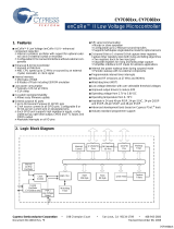
Internal
24 MHz
Oscillator
3.3V
Regulator
Clock
Control
POR /
Low-Voltage
Detect
Watchdog
Timer
RAM
Up to 256
Byte
M8C CPU
Flash
Up to 8K
Byte
Up to 14
Extended
IO Pins
Low-Speed
USB/PS2
Transceiver
and Pull up
Up to 6
GPIO
pins
Wakeup
Timer
16-bit Free
running
timer
12-bit Timer
4 3VIO/SPI
Pins
Vdd
Interrupt
Control
Low-Speed
USB SIE
External Clock
2. Logic Block Diagram
[+] Feedback [+] Feedback

CY7C63310, CY7C638xx
Document 38-08035 Rev. *K Page 3 of 83
3. Introduction
Cypress has reinvented its leadership position in the low speed
USB market with a new family of innovative microcontrollers.
Introducing enCoRe II USB - “enhanced Component Reduction.”
Cypress has leveraged its design expertise in USB solutions to
advance its family of low speed USB microcontrollers, which
enable peripheral developers to design new products with a
minimum number of components. The enCoRe II USB
technology builds on the enCoRe family. The enCoRe family has
an integrated oscillator that eliminates the external crystal or
resonator, reducing overall cost. Also integrated into this chip are
other external components commonly found in low speed USB
applications, such as pull up resistors, wakeup circuitry, and a
3.3V regulator. Integrating these components reduces the
overall system cost.
The enCoRe II is an 8-bit Flash programmable microcontroller
with an integrated low speed USB interface. The instruction set
is optimized specifically for USB and PS/2 operations, although
the microcontrollers may be used for a variety of other embedded
applications.
The enCoRe II features up to 20 GPIO pins to support USB,
PS/2, and other applications. The IO pins are grouped into four
ports (Port 0 to 3). The pins on Port 0 and Port 1 may each be
configured individually while the pins on Ports 2 and 3 are
configured only as a group. Each GPIO port supports high
impedance inputs, configurable pull up, open drain output,
CMOS/TTL inputs, and CMOS output with up to five pins that
support a programmable drive strength of up to 50 mA sink
current. GPIO Port 1 features four pins that interface at a voltage
level of 3.3V. Additionally, each IO pin may be used to generate
a GPIO interrupt to the microcontroller. Each GPIO port has its
own GPIO interrupt vector; in addition, GPIO Port 0 has three
dedicated pins that have independent interrupt vectors (P0.2 -
P0.4).
The enCoRe II features an internal oscillator. With the presence
of USB traffic, the internal oscillator may be set to precisely tune
to USB timing requirements (24 MHz ±1.5%). Optionally, an
external 12 MHz or 24 MHz clock is used to provide a higher
precision reference for USB operation. The clock generator
provides the 12 MHz and 24 MHz clocks that remain internal to
the microcontroller. The enCoRe II also has a 12-bit program-
mable interval timer and a 16-bit Free Running Timer with
Capture Timer registers. In addition, the enCoRe II includes a
Watchdog timer and a vectored interrupt controller.
The enCoRe II has up to eight Kbytes of Flash for user code and
up to 256 bytes of RAM for stack space and user variables.
The power on reset circuit detects logic when power is applied
to the device, resets the logic to a known state, and begins
executing instructions at Flash address 0x0000. When power
falls below a programmable trip voltage, it generates a reset or
may be configured to generate an interrupt. There is a low
voltage detect circuit that detects when V
CC
drops below a
programmable trip voltage. It is configurable to generate an LVD
interrupt to inform the processor about the low voltage event.
POR and LVD share the same interrupt. There is no separate
interrupt for each. The Watchdog timer may be used to ensure
the firmware never gets stalled in an infinite loop.
The microcontroller supports 22 maskable interrupts in the
vectored interrupt controller. Interrupt sources include a USB bus
reset, LVR/POR, a programmable interval timer, a 1.024 ms
output from the free-running timer, three USB endpoints, two
capture timers, four GPIO Ports, three Port 0 pins, two SPI, a
16-bit free running timer wrap, an internal sleep timer, and a bus
active interrupt. The sleep timer causes periodic interrupts when
enabled. The USB endpoints interrupt after a USB transaction
complete is on the bus. The capture timers interrupt when a new
timer value is saved because of a selected GPIO edge event. A
total of seven GPIO interrupts support both TTL or CMOS
thresholds. For additional flexibility on the edge sensitive GPIO
pins, the interrupt polarity is programmed as rising or falling.
The free-running 16-bit timer provides two interrupt sources: the
1.024 ms outputs and the free running counter wrap interrupt.
The programmable interval timer provides up to 1 μsec
resolution and provides an interrupt every time it expires. These
timers are used to measure the duration of an event under
firmware control by reading the desired timer at the start and at
the end of an event, then calculating the difference between the
two values. The two 8-bit capture timer registers save a
programmable 8-bit range of the free-running timer when a GPIO
edge occurs on the two capture pins (P0.5, P0.6). The two 8-bit
captures may be ganged into a single 16-bit capture.
The enCoRe II includes an integrated USB serial interface
engine (SIE) that allows the chip to easily interface to a USB
host. The hardware supports one USB device address with three
endpoints.
The USB D+ and D– pins are optionally used as PS/2 SCLK and
SDATA signals so that products are designed to respond to
either USB or PS/2 modes of operation. The PS/2 operation is
supported with internal 5 KΩ pull up resistors on P1.0 (D+) and
P1.1 (D–), and an interrupt to signal the start of PS/2 activity. In
USB mode, the integrated 1.5 KΩ pull up resistor on D– may be
controlled under firmware. No external components are
necessary for dual USB and PS/2 systems, and no GPIO pins
need to be dedicated to switching between modes.
The enCoRe II supports in system programming by using the D+
and D– pins as the serial programming mode interface. The
programming protocol is not USB.
4. Conventions
In this data sheet, bit positions in the registers are shaded to
indicate which members of the enCoRe II family implement the
bits.
Available in all enCoRe II family members
CY7C638(1/2/3)3 only
[+] Feedback [+] Feedback

CY7C63310, CY7C638xx
Document 38-08035 Rev. *K Page 4 of 83
5. Pinouts
Figure 5-1. Pin Diagrams
1
2
3
4
5
6
9
11
15
16
17
18
19
20
22
21
NC
P0.7
TIO1/P0.6
TIO0/P0.5
INT2/P0.4
INT1/P0.3
P0.0
P2.0
P1.5/SMOSI
P1.3/SSEL
P3.1
P3.0
V
CC
P1.2/VREG
P1.1/D–
P1.0/D+
14
P1.4/SCLK
10
P2.1
NC
V
SS
12
13
7
8
INT0/P0.2
P0.1
24
23
P1.7
P1.6/SMISO
24-Pin QSOP
CY7C63823
1
2
3
4
6
7
8
10
11
12
13
15
16
18
17
SSEL/P1.3
SCLK/P1.4
SMOSI/P1.5
SMISO/P1.6
P0.7
TIO0/P0.5
P1.2/VREG
P1.1/D–
P1.0/D+
P0.0
P0.1
P0.2/INT0
18-Pin PDIP
V
CC
9
TIO1/P0.6
INT2/P0.4
P0.3/INT1
CY7C63813
5
14
P1.7
V
SS
1
2
3
4
6
7
8
9
10
11
13
14
16
15
SSEL/P1.3
SCLK/P1.4
SMOSI/P1.5
SMISO/P1.6
TIO0/P0.5
INT1/P0.3
P1.2
P1.1/D–
P1.0/D+
P0.1
P0.2/INT0
P0.0
16-Pin PDIP
V
CC
INT2/P0.4
5
12
TIO1/P0.6
V
SS
Top View
CY7C63801, CY7C63310
1
2
3
4
6
7
8
9
10
11
13
14
16
15
TIO1/P0.6
TIO0/P0.5
INT2/P0.4
INT1/P0.3
P0.1
V
SS
P1.6/SMISO
P1.4/SCLK
P1.3/SSEL
P1.1/D–
P1.0/D+
V
CC
16-Pin SOIC
P1.5/SMOSI
P0.0
5
12
INT0/P0.2
P1.2
CY7C63801, CY7C63310
1
2
3
4
6
7
8
10
11
12
13
15
16
18
17
P0.7
TIO1/P0.6
TIO0/P0.5
INT2/P0.4
INT0/P0.2
P0.0
P1.7
P1.5/SMOSI
P1.4/SCLK
P1.2/VREG
V
CC
P1.1/D–
18-Pin SOIC
P1.6/SMISO
9
P0.1
V
SS
P1.0/D+
CY7C63813
5
14
INT1/P0.3
P1.3/SSEL
1
2
3
4
5
6
9
11
15
16
17
18
19
20
22
21
NC
P0.7
TIO1/P0.6
TIO0/P0.5
INT2/P0.4
INT1/P0.3
P0.0
P2.0
P1.6/SMISO
P3.0
P1.4/SCLK
P3.1
P1.2/VREG
P1.3/SSEL
V
CC
P1.1/D–
14
P1.5/SMOSI
10
P2.1
V
SS
P1.0/D+
12
13
7
8
INT0/P0.2
P0.1
24
23
NC
P1.7
24-Pin SOIC
CY7C63823
1
2
3
4
6
7
8
9
10
11
13
14
16
15
TIO1/P0.6
TIO0/P0.5
INT2/P0.4
INT1/P0.3
P0.1
V
SS
P1.6/SMISO
P1.4/SCLK
P1.3/SSEL
P1.1/D–
P1.0/D+
V
CC
P1.5/SMOSI
P0.0
5
12
INT0/P0.2
P1.2/VREG
CY7C63803
16-Pin SOIC
1
2
3
4
5
6
21
19
23
25
22
26
20
24
18
9
8
12 1310 14 1611
17
15
7
272832
30 29
31
P0.6/TIO1
P0.5/TIO0
P0.4/INT2
P0.3/INT1
P0.2/INT0
P0.1
P0.0
P2.1
P2.0
NC
NC
NC
Vss
P1.0/D+
P1.1/D-
Vdd
NC
NC
P1.3/SSEL
P3.0
P3.1
P1.4/SCLK
P1.5/SMOSI
P1.6/MISO
P1.7
P0.7
NC
NC
NC
NC
NC
P1.2/VREG
1
2
3
4
5
6
21
19
23
25
22
26
20
24
18
9
8
12 1310 14 1611
17
15
7
272832
30 29
31
P0.6/TIO1
P0.5/TIO0
P0.4/INT2
P0.3/INT1
P0.2/INT0
P0.1
P0.0
P2.1
P2.0
NC
NC
NC
Vss
P1.0/D+
P1.1/D-
Vdd
NC
NC
P1.3/SSEL
P3.0
P3.1
P1.4/SCLK
P1.5/SMOSI
P1.6/MISO
P1.7
P0.7
NC
NC
NC
NC
NC
P1.2/VREG
32-Pin QFN
CY7C63833
CY7C63833 32-Pin Sawn QFN
[+] Feedback [+] Feedback

CY7C63310, CY7C638xx
Document 38-08035 Rev. *K Page 5 of 83
Figure 5-2. CY7C63823 Die Form
Die step = 1792 .98 μm x 2272.998 μm
Die size = 1727 μm x 2187 μm
Bond pad opening = 70 μm x 70 μm
Die thickness = 14 mils
Legend
1
2
4
3
5
6
8
7
9
10 11
12
13
14
15
16
17
18
19
20
21
22
23
Cypress Logo
X
Y
Table 5-1. Die Pad Summary
Pad Number Pad Name X (microns) Y (microns)
1 P0.7 -742.730 911.990
2 P0.6 -755.060 792.200
3 P0.5 -755.060 699.300
4 P0.4 -755.060 606.400
5 P0.3 -755.060 -430.080
6 P0.2 -755.060 -522.980
7 P0.1 -755.060 -618.830
8 P0.0 CLKIN -755.060 -714.020
9 P2.1 -755.060 -810.220
10 P2.0 -393.580 -977.930
11 VSS 537.500 -964.700
12 PI.0 D+ 736.110 -936.680
13 P1.1 D– 736.110 -625.130
14 VDD 736.110 -260.670
15 P1.2 VREG 736.110 53.800
16 P1.3 723.510 336.780
17 P3.0 723.510 438.690
18 P3.1 723.510 532.880
19 P1.4 723.510 635.310
20 P1.5 SMOSI 723.510 728.220
21 P1.6 SMISO 723.510 839.290
22 P1.7 696.630 1008.480
23 Reserved -795.400 1023.270
[+] Feedback [+] Feedback

CY7C63310, CY7C638xx
Document 38-08035 Rev. *K Page 6 of 83
Table 5-2. Pin Description
32
QFN
24
QSOP
24
SOIC
18
SIOC
18
PDIP
16
SOIC
16
PDIP
Name Description
21 19 18 P3.0 GPIO Port 3. Configured as a group (byte).
22 20 19 P3.1
91111 P2.0GPIO Port 2. Configured as a group (byte).
81010 P2.1
14 14 13 10 15 9 13 P1.0/D+ GPIO Port 1 bit 0/USB D+
[1]
If this pin is used as a
General Purpose output, it draws current. This pin
must be configured as an input to reduce current
draw.
15 15 14 11 16 10 14 P1.1/D– GPIO Port 1 bit 1/USB D–
[1]
If this pin is used as a
General Purpose output, it draws current. This pin
must be configured as an input to reduce current
draw.
18 17 16 13 18 12 16 P1.2/VREG GPIO Port 1 bit 2. Configured individually.
3.3V if regulator is enabled. (The 3.3V regulator is not
available in the CY7C63310 and CY7C63801.) A 1-μF
min, 2-μF max capacitor is required on Vreg output.
20 18 17 14 1 13 1 P1.3/SSEL GPIO Port 1 bit 3. Configured individually.
Alternate function is SSEL signal of the SPI bus TTL
voltage thresholds. Although Vreg is not available
with the CY7C63310, 3.3V IO is still available.
23 21 20 15 2 14 2 P1.4/SCLK GPIO Port 1 bit 4. Configured individually.
Alternate function is SCLK signal of the SPI bus TTL
voltage thresholds. Although Vreg is not available
with the CY7C63310, 3.3V IO is still available.
24 22 21 16 3 15 3 P1.5/SMOSI GPIO Port 1 bit 5. Configured individually.
Alternate function is SMOSI signal of the SPI bus TTL
voltage thresholds. Although Vreg is not available
with the CY7C63310, 3.3V IO is still available.
25 23 22 17 4 16 4 P1.6/SMISO GPIO Port 1 bit 6. Configured individually.
Alternate function is SMISO signal of the SPI bus TTL
voltage thresholds. Although Vreg is not available
with the CY7C63310, 3.3V IO is still available.
26 24 23 18 5 P1.7 GPIO Port 1 bit 7. Configured individually.
TTL voltage threshold.
7 9 9 8 13 7 11 P0.0 GPIO Port 0 bit 0. Configured individually.
On CY7C638xx and CY7C63310, external clock
input when configured as Clock In.
6 8 8 7 12 6 10 P0.1 GPIO Port 0 bit 1. Configured individually.
On CY7C638xx and CY7C63310, clock output when
configured as Clock Out.
57761159P0.2/INT0GPIO Port 0 bit 2. Configured individually.
Optional rising edge interrupt INT0.
46651048P0.3/INT1GPIO Port 0 bit 3. Configured individually.
Optional rising edge interrupt INT1.
3 5 5 4 9 3 7 P0.4/INT2 GPIO Port 0 bit 4. Configured individually.
Optional rising edge interrupt INT2.
Note
1. P1.0(D+) and P1.1(D–) pins must be in IO mode when used as GPIO and in I
sb
mode.
[+] Feedback [+] Feedback

CY7C63310, CY7C638xx
Document 38-08035 Rev. *K Page 7 of 83
6. CPU Architecture
This family of microcontrollers is based on a high performance,
8-bit, Harvard architecture microprocessor. Five registers control
the primary operation of the CPU core. These registers are
affected by various instructions, but are not directly accessible
through the register space by the user.
The 16-bit Program Counter Register (CPU_PC) allows direct
addressing of the full 8 Kbytes of program memory space.
The Accumulator Register (CPU_A) is the general purpose
register, which holds the results of instructions that specify any
of the source addressing modes.
The Index Register (CPU_X) holds an offset value that is used
in the indexed addressing modes. Typically, this is used to
address a block of data within the data memory space.
The Stack Pointer Register (CPU_SP) holds the address of the
current top of the stack in the data memory space. It is affected
by the PUSH, POP, LCALL, CALL, RETI, and RET instructions,
which manage the software stack. It is also affected by the SWAP
and ADD instructions.
The Flag Register (CPU_F) has three status bits: Zero Flag bit
[1]; Carry Flag bit [2]; Supervisory State bit [3]. The Global
Interrupt Enable bit [0] globally enables or disables interrupts.
The user cannot manipulate the Supervisory State status bit [3].
The flags are affected by arithmetic, logic, and shift operations.
The manner in which each flag is changed is dependent upon
the instruction being executed, such as AND, OR, XOR, and
others. See Table 8-1 on page 12.
2 4 4 3 8 2 6 P0.5/TIO0 GPIO Port 0 bit 5. Configured individually
Alternate function Timer capture inputs or Timer
output TIO0
1 3 3 2 7 1 5 P0.6/TIO1 GPIO Port 0 bit 6. Configured individually
Alternate function Timer capture inputs or Timer
output TIO1
32 2 2 1 6 P0.7 GPIO Port 0 bit 7. Configured individually
Not present in the 16 pin PDIP or SOIC package
10 1 1 NC No connect
11 12 24 NC No connect
12 NC No connect
17 NC No connect
19 NC No connect
27 NC No connect
28 NC No connect
29 NC No connect
30 NC No connect
31 NC No connect
16 16 15 12 17 11 15 Vcc Supply
13 13 12 9 14 8 12 V
SS
Ground
Table 5-2. Pin Description (continued)
32
QFN
24
QSOP
24
SOIC
18
SIOC
18
PDIP
16
SOIC
16
PDIP
Name Description
Table 6-1. CPU Registers and Register Names
CPU Register Register Name
Flags CPU_F
Program Counter CPU_PC
Accumulator CPU_A
Stack Pointer CPU_SP
Index CPU_X
[+] Feedback [+] Feedback

CY7C63310, CY7C638xx
Document 38-08035 Rev. *K Page 8 of 83
7. CPU Registers
The CPU registers in enCoRe II devices are in two banks with 256 registers in each bank. Bit[4]/XIO bit in the CPU Flags register
must be set/cleared to select between the two register banks Table 7-1 on page 8
7.1 Flags Register
The Flags Register is set or reset only with logical instruction.
Table 7-1. CPU Flags Register (CPU_F) [R/W]
Bit # 7 6 5 4 3 2 1 0
Field Reserved XIO Super Carry Zero Global IE
Read/Write – – – R/W R RW RW RW
Default 00000010
Bit [7:5]: Reserved
Bit 4: XIO
Set by the user to select between the register banks
0 = Bank 0
1 = Bank 1
Bit 3: Super
Indicates whether the CPU is executing user code or Supervisor Code. (This code cannot be accessed directly by the user.)
0 = User Code
1 = Supervisor Code
Bit 2: Carry
Set by the CPU to indicate whether there has been a carry in the previous logical/arithmetic operation.
0 = No Carry
1 = Carry
Bit 1: Zero
Set by the CPU to indicate whether there has been a zero result in the previous logical/arithmetic operation.
0 = Not Equal to Zero
1 = Equal to Zero
Bit 0: Global IE
Determines whether all interrupts are enabled or disabled
0 = Disabled
1 = Enabled
Note CPU_F register is only readable with the explicit register address 0xF7. The OR F, expr and AND F, expr instructions must
be used to set and clear the CPU_F bits.
Table 7-2. CPU Accumulator Register (CPU_A)
Bit # 7 6 5 4 3 2 1 0
Field CPU Accumulator [7:0]
Read/Write ––––––––
Default 00000000
Bit [7:0]: CPU Accumulator [7:0]
8-bit data value holds the result of any logical/arithmetic instruction that uses a source addressing mode
[+] Feedback [+] Feedback

CY7C63310, CY7C638xx
Document 38-08035 Rev. *K Page 9 of 83
7.2 Addressing Modes
7.2.1 Source Immediate
The result of an instruction using this addressing mode is placed
in the A register, the F register, the SP register, or the X register,
which is specified as part of the instruction opcode. Operand 1
is an immediate value that serves as a source for the instruction.
Arithmetic instructions require two sources; the second source is
the A or the X register specified in the opcode. Instructions using
this addressing mode are two bytes in length.
Examples
Table 7-3. CPU X Register (CPU_X)
Bit # 7 6 5 4 3 2 1 0
Field X [7:0]
Read/Write ––––––––
Default 00000000
Bit [7:0]: X [7:0]
8-bit data value holds an index for any instruction that uses an indexed addressing mode.
Table 7-4. CPU Stack Pointer Register (CPU_SP)
Bit # 7 6 5 4 3 2 1 0
Field Stack Pointer [7:0]
Read/Write ––––––––
Default 00000000
Bit [7:0]: Stack Pointer [7:0]
8-bit data value holds a pointer to the current top of the stack.
Table 7-5. CPU Program Counter High Register (CPU_PCH)
Bit # 7 6 5 4 3 2 1 0
Field Program Counter [15:8]
Read/Write ––––––––
Default 00000000
Bit [7:0]: Program Counter [15:8]
8-bit data value holds the higher byte of the program counter.
Table 7-6. CPU Program Counter Low Register (CPU_PCL)
Bit # 7 6 5 4 3 2 1 0
Field Program Counter [7:0]
Read/Write ––––––––
Default 00000000
Bit [7:0]: Program Counter [7:0]
8-bit data value holds the lower byte of the program counter.
Table 7-7. Source Immediate
Opcode Operand 1
Instruction Immediate Value
ADD A 7 The immediate value of 7 is added with the
Accumulator and the result is placed in the
Accumulator.
MOV X 8 The immediate value of 8 is moved to the X
register.
AND F 9 The immediate value of 9 is logically ANDed with
the F register and the result is placed in the F
register.
[+] Feedback [+] Feedback

CY7C63310, CY7C638xx
Document 38-08035 Rev. *K Page 10 of 83
7.2.2 Source Direct
The result of an instruction using this addressing mode is placed
in either the A register or the X register, which is specified as part
of the instruction opcode. Operand 1 is an address that points to
a location in the RAM memory space or the register space that
is the source of the instruction. Arithmetic instructions require
two sources; the second source is the A register or X register
specified in the opcode. Instructions using this addressing mode
are two bytes in length.
Examples
7.2.3 Source Indexed
The result of an instruction using this addressing mode is placed
in either the A register or the X register, which is specified as part
of the instruction opcode. Operand 1 is added to the X register
forming an address that points to a location in the RAM memory
space or the register space that is the source of the instruction.
Arithmetic instructions require two sources; the second source is
the A register or X register specified in the opcode. Instructions
using this addressing mode are two bytes in length.
Examples
7.2.4 Destination Direct
The result of an instruction using this addressing mode is placed
within the RAM memory space or the register space. Operand 1
is an address that points to the location of the result. The source
for the instruction is either the A register or the X register, which
is specified as part of the instruction opcode. Arithmetic instruc-
tions require two sources; the second source is the location
specified by Operand 1. Instructions using this addressing mode
are two bytes in length.
Examples
7.2.5 Destination Indexed
The result of an instruction using this addressing mode is placed
within the RAM memory space or the register space. Operand 1
is added to the X register forming the address that points to the
location of the result. The source for the instruction is the A
register. Arithmetic instructions require two sources; the second
source is the location specified by Operand 1 added with the X
register. Instructions using this addressing mode are two bytes
in length.
Example
Table 7-8. Source Direct
Opcode Operand 1
Instruction Source Address
ADD A [7] The value in the RAM memory location at
address 7 is added with the Accumulator,
and the result is placed in the Accumu-
lator.
MOV X REG[8] The value in the register space at address
8 is moved to the X register.
Table 7-9. Source Indexed
Opcode Operand 1
Instruction Source Index
ADD A [X+7] The value in the memory location at
address X + 7 is added with the
Accumulator, and the result is placed
in the Accumulator.
MOV X REG[X+8] The value in the register space at
address X + 8 is moved to the X
register.
Table 7-10. Destination Direct
Opcode Operand 1
Instruction Destination Address
ADD [7] A The value in the memory location at
address 7 is added with the Accumu-
lator, and the result is placed in the
memory location at address 7. The
Accumulator is unchanged.
MOV REG[8] A The Accumulator is moved to the
register space location at address 8.
The Accumulator is unchanged.
Table 7-11. Destination Indexed
Opcode Operand 1
Instruction Destination Index
ADD [X+7] A The value in the; memory location at
address X+7 is added with the Accumu-
lator, and the result is placed in the
memory location at address x+7. The
Accumulator is unchanged.
[+] Feedback [+] Feedback

CY7C63310, CY7C638xx
Document 38-08035 Rev. *K Page 11 of 83
7.2.6 Destination Direct Source Immediate
The result of an instruction using this addressing mode is placed
within the RAM memory space or the register space. Operand 1
is the address of the result. The source of the instruction is
Operand 2, which is an immediate value. Arithmetic instructions
require two sources; the second source is the location specified
by Operand 1. Instructions using this addressing mode are three
bytes in length.
Examples
7.2.7 Destination Indexed Source Immediate
The result of an instruction using this addressing mode is placed
within the RAM memory space or the register space. Operand 1
is added to the X register to form the address of the result. The
source of the instruction is Operand 2, which is an immediate
value. Arithmetic instructions require two sources; the second
source is the location specified by Operand 1 added with the X
register. Instructions using this addressing mode are three bytes
in length.
Examples
7.2.8 Destination Direct Source Direct
The result of an instruction using this addressing mode is placed
within the RAM memory. Operand 1 is the address of the result.
Operand 2 is an address that points to a location in the RAM
memory that is the source for the instruction. This addressing
mode is only valid on the MOV instruction. The instruction using
this addressing mode is three bytes in length.
.
Example
7.2.9 Source Indirect Post Increment
The result of an instruction using this addressing mode is placed
in the Accumulator. Operand 1 is an address pointing to a
location within the memory space, which contains an address
(the indirect address) for the source of the instruction. The
indirect address is incremented as part of the instruction
execution. This addressing mode is only valid on the MVI
instruction. The instruction using this addressing mode is two
bytes in length. Refer to the PSoC Designer: Assembly
Language User Guide for further details on MVI instruction.
Example
7.2.10 Destination Indirect Post Increment
The result of an instruction using this addressing mode is placed
within the memory space. Operand 1 is an address pointing to a
location within the memory space, which contains an address
(the indirect address) for the destination of the instruction. The
indirect address is incremented as part of the instruction
execution. The source for the instruction is the Accumulator. This
addressing mode is only valid on the MVI instruction. The
instruction using this addressing mode is two bytes in length.
Example
Table 7-12. Destination Direct Source Immediate
Opcode Operand 1 Operand 2
Instruction Destination Address Immediate Value
ADD [7] 5
The value in the memory location at address
7 is added to the immediate value of 5, and
the result is placed in the memory location at
address 7.
MOV REG[8] 6 The immediate value of 6 is moved into the
register space location at address 8.
Table 7-13. Destination Indexed Source Immediate
Opcode Operand 1 Operand 2
Instruction Destination Index Immediate Value
ADD [X+7] 5 The value in the memory location at
address X+7 is added with the
immediate value of 5, and the result
is placed in the memory location at
address X+7.
MOV REG[X+8] 6 The immediate value of 6 is moved
into the location in the register space
at address X+8.
Table 7-14. Destination Direct Source Direct
Opcode Operand 1 Operand 2
Instruction Destination Address Source Address
MOV [7] [8] The value in the memory location at address 8
is moved to the memory location at address 7.
Table 7-15. Source Indirect Post Increment
Opcode Operand 1
Instruction Source Address Address
MVI A [8] The value in the memory location at address
8 is an indirect address. The memory location
pointed to by the indirect address is moved
into the Accumulator. The indirect address is
then incremented.
Table 7-16. Destination Indirect Post Increment
Opcode Operand 1
Instruction Destination Address Address
MVI [8] A The value in the memory location at
address 8 is an indirect address. The
Accumulator is moved into the memory
location pointed to by the indirect
address. The indirect address is then
incremented.
[+] Feedback [+] Feedback

CY7C63310, CY7C638xx
Document 38-08035 Rev. *K Page 12 of 83
8. Instruction Set Summary
The instruction set is summarized in Ta b l e 8-1 numerically and serves as a quick reference. If more information is needed, the
Instruction Set Summary tables are described in detail in the PSoC Designer Assembly Language User Guide (available on the
Cypress web site at http://www.cypress.com).
Table 8-1. Instruction Set Summary Sorted Numerically by Opcode Order
[2, 3]
Opcode Hex
Cycles
Bytes
Instruction Format Flags
Opcode Hex
Cycles
Bytes
Instruction Format Flags
Opcode Hex
Cycles
Bytes
Instruction Format Flags
00 15 1 SSC 2D 8 2 OR [X+expr], A Z 5A 5 2 MOV [expr], X
01 4 2 ADD A, expr C, Z 2E 9 3 OR [expr], expr Z 5B 4 1 MOV A, X Z
02 6 2 ADD A, [expr] C, Z 2F 10 3 OR [X+expr], expr Z 5C 4 1 MOV X, A
03 7 2 ADD A, [X+expr] C, Z 30 9 1 HALT 5D 6 2 MOV A, reg[expr] Z
04 7 2 ADD [expr], A C, Z 31 4 2 XOR A, expr Z 5E 7 2 MOV A, reg[X+expr] Z
05 8 2 ADD [X+expr], A C, Z 32 6 2 XOR A, [expr] Z 5F 10 3 MOV [expr], [expr]
06 9 3 ADD [expr], expr C, Z 33 7 2 XOR A, [X+expr] Z 60 5 2 MOV reg[expr], A
07 10 3 ADD [X+expr], expr C, Z 34 7 2 XOR [expr], A Z 61 6 2 MOV reg[X+expr], A
08 4 1 PUSH A 35 8 2 XOR [X+expr], A Z 62 8 3 MOV reg[expr], expr
09 4 2 ADC A, expr C, Z 36 9 3 XOR [expr], expr Z 63 9 3 MOV reg[X+expr], expr
0A 6 2 ADC A, [expr] C, Z 37 10 3 XOR [X+expr], expr Z 64 4 1 ASL A C, Z
0B 7 2 ADC A, [X+expr] C, Z 38 5 2 ADD SP, expr 65 7 2 ASL [expr] C, Z
0C 7 2 ADC [expr], A C, Z 39 5 2 CMP A, expr
if (A=B) Z=1
if (A<B) C=1
66 8 2 ASL [X+expr] C, Z
0D 8 2 ADC [X+expr], A C, Z 3A 7 2 CMP A, [expr] 67 4 1 ASR A C, Z
0E 9 3 ADC [expr], expr C, Z 3B 8 2 CMP A, [X+expr] 68 7 2 ASR [expr] C, Z
0F 10 3 ADC [X+expr], expr C, Z 3C 8 3 CMP [expr], expr 69 8 2 ASR [X+expr] C, Z
10 4 1 PUSH X 3D 9 3 CMP [X+expr], expr 6A 4 1 RLC A C, Z
11 4 2 SUB A, expr C, Z 3E 10 2 MVI A, [ [expr]++] Z 6B 7 2 RLC [expr] C, Z
12 6 2 SUB A, [expr] C, Z 3F 10 2 MVI [ [expr]++], A 6C 8 2 RLC [X+expr] C, Z
13 7 2 SUB A, [X+expr] C, Z 40 4 1 NOP 6D 4 1 RRC A C, Z
14 7 2 SUB [expr], A C, Z 41 9 3 AND reg[expr], expr Z 6E 7 2 RRC [expr] C, Z
15 8 2 SUB [X+expr], A C, Z 42 10 3 AND reg[X+expr], expr Z 6F 8 2 RRC [X+expr] C, Z
16 9 3 SUB [expr], expr C, Z 43 9 3 OR reg[expr], expr Z 70 4 2 AND F, expr C, Z
17 10 3 SUB [X+expr], expr C, Z 44 10 3 OR reg[X+expr], expr Z 71 4 2 OR F, expr C, Z
18 5 1 POP A Z 45 9 3 XOR reg[expr], expr Z 72 4 2 XOR F, expr C, Z
19 4 2 SBB A, expr C, Z 46 10 3 XOR reg[X+expr], expr Z 73 4 1 CPL A Z
1A 6 2 SBB A, [expr] C, Z 47 8 3 TST [expr], expr Z 74 4 1 INC A C, Z
1B 7 2 SBB A, [X+expr] C, Z 48 9 3 TST [X+expr], expr Z 75 4 1 INC X C, Z
1C 7 2 SBB [expr], A C, Z 49 9 3 TST reg[expr], expr Z 76 7 2 INC [expr] C, Z
1D 8 2 SBB [X+expr], A C, Z 4A 10 3 TST reg[X+expr], expr Z 77 8 2 INC [X+expr] C, Z
1E 9 3 SBB [expr], expr C, Z 4B 5 1 SWAP A, X Z 78 4 1 DEC A C, Z
1F 10 3 SBB [X+expr], expr C, Z 4C 7 2 SWAP A, [expr] Z 79 4 1 DEC X C, Z
20 5 1 POP X 4D 7 2 SWAP X, [expr] 7A 7 2 DEC [expr] C, Z
21 4 2 AND A, expr Z 4E 5 1 SWAP A, SP Z 7B 8 2 DEC [X+expr] C, Z
22 6 2 AND A, [expr] Z 4F 4 1 MOV X, SP 7C 13 3 LCALL
23 7 2 AND A, [X+expr] Z 50 4 2 MOV A, expr Z 7D 7 3 LJMP
24 7 2 AND [expr], A Z 51 5 2 MOV A, [expr] Z 7E 10 1 RETI C, Z
25 8 2 AND [X+expr], A Z 52 6 2 MOV A, [X+expr] Z 7F 8 1 RET
26 9 3 AND [expr], expr Z 53 5 2 MOV [expr], A 8x 5 2 JMP
27 10 3 AND [X+expr], expr Z 54 6 2 MOV [X+expr], A 9x 11 2 CALL
28 11 1 ROMX Z 55 8 3 MOV [expr], expr Ax 5 2 JZ
29 4 2 OR A, expr Z 56 9 3 MOV [X+expr], expr Bx 5 2 JNZ
2A 6 2 OR A, [expr] Z 57 4 2 MOV X, expr Cx 5 2 JC
2B 7 2 OR A, [X+expr] Z 58 6 2 MOV X, [expr] Dx 5 2 JNC
2C 7 2 OR [expr], A Z 59 7 2 MOV X, [X+expr] Ex 7 2 JACC
Fx 13 2 INDEX Z
Notes
2. Interrupt routines take 13 cycles before execution resumes at interrupt vector table.
3. The number of cycles required by an instruction is increased by one for instructions that span 256 byte boundaries in the Flash memory space.
[+] Feedback [+] Feedback

CY7C63310, CY7C638xx
Document 38-08035 Rev. *K Page 13 of 83
9. Memory Organization
9.1 Flash Program Memory Organization
Figure 9-1. Program Memory Space with Interrupt Vector Table
after reset Address
16-bit PC 0x0000 Program execution begins here after a reset
0x0004 POR/LVD
0x0008 INT0
0x000C SPI Transmitter Empty
0x0010 SPI Receiver Full
0x0014 GPIO Port 0
0x0018 GPIO Port 1
0x001C INT1
0x0020 EP0
0x0024 EP1
0x0028 EP2
0x002C USB Reset
0x0030 USB Active
0x0034 1 ms Interval timer
0x0038 Programmable Interval Timer
0x003C Timer Capture 0
0x0040 Timer Capture 1
0x0044 16-bit Free Running Timer Wrap
0x0048 INT2
0x004C PS2 Data Low
0x0050 GPIO Port 2
0x0054 GPIO Port 3
0x0058 Reserved
0x005C Reserved
0x0060 Reserved
0x0064 Sleep Timer
0x0068 Program Memory begins here (if below interrupts not used,
program memory can start lower)
0x0BFF 3 KB ends here (CY7C63310)
0x0FFF 4 KB ends here (CY7C63801)
0x1FFF 8 KB ends here (CY7C638x3)
[+] Feedback [+] Feedback

CY7C63310, CY7C638xx
Document 38-08035 Rev. *K Page 14 of 83
9.2 Data Memory Organization
The CY7C63310/638xx microcontrollers provide up to 256 bytes of data RAM.
9.3 Flash
This section describes the Flash block of the enCoRe II. Much of
the user visible Flash functionality including programming and
security are implemented in the M8C Supervisory Read Only
Memory (SROM). The enCoRe II Flash has an endurance of
1000 cycles and a 10 year data retention capability.
9.3.1 Flash Programming and Security
All Flash programming is performed by code in the SROM. The
registers that control the Flash programming are only visible to
the M8C CPU when it executes out of SROM. This makes it
impossible to read, write or erase the Flash by bypassing the
security mechanisms implemented in the SROM.
Customer firmware can program the Flash only through SROM
calls. The data or code images are sourced through any interface
with the appropriate support firmware. This type of programming
requires a ‘boot-loader’, which is a piece of firmware resident on
the Flash. For safety reasons this boot-loader must not be
overwritten during firmware rewrites.
The Flash provides four extra auxiliary rows that are used to hold
Flash block protection flags, boot time calibration values,
configuration tables, and any device values. The routines for
accessing these auxiliary rows are documented in the section
SROM on page 14 section. The auxiliary rows are not affected
by the device erase function.
9.3.2 In System Programming
Most designs that include an enCoRe II part have a USB
connector attached to the USB D+ and D– pins on the device.
These designs require the ability to program or reprogram a part
through the USB D+ and D– pins alone.
The enCoRe II devices enable this type of in system
programming by using the D+ and D– pins as the serial
programming mode interface. This allows an external controller
to enable the enCoRe II part to enter the serial programming
mode, and then use the test queue to issue Flash access
functions in the SROM. The programming protocol is not USB.
9.4 SROM
The SROM holds code that boots the part, calibrates circuitry,
and performs Flash operations (Table 9-1 on page 14 lists the
SROM functions). The functions of the SROM are accessed in
the normal user code or operating from Flash. The SROM exists
in a separate memory space from the user code. The SROM
functions are accessed by executing the Supervisory System
Call instruction (SSC), which has an opcode of 00h. Before
executing the SSC the M8C’s accumulator must be loaded with
the desired SROM function code from Table 9-1 on page 14.
Undefined functions cause a HALT if called from the user code.
The SROM functions are executing code with calls; as a result,
the functions require stack space. With the exception of Reset,
all of the SROM functions have a parameter block in SRAM that
must be configured before executing the SSC. Table 9-2 on page
15 lists all possible parameter block variables. The meaning of
each parameter, with regards to a specific SROM function, is
described later in this section.
Figure 9-2. Data Memory Organization
after reset Address
8-bit PSP 0x00 Stack begins here and grows upward.
Top of RAM Memory 0xFF
Table 9-1. SROM Function Codes
Function Code Function Name Stack Space
00h SWBootReset 0
01h ReadBlock 7
02h WriteBlock 10
03h EraseBlock 9
05h EraseAll 11
06h TableRead 3
07h CheckSum 3
[+] Feedback [+] Feedback

CY7C63310, CY7C638xx
Document 38-08035 Rev. *K Page 15 of 83
Two important variables that are used for all functions are KEY1
and KEY2. These variables are used to help discriminate
between valid SSCs and inadvertent SSCs. KEY1 must always
have a value of 3Ah, while KEY2 must have the same value as
the stack pointer when the SROM function begins execution.
This would be the Stack Pointer value when the SSC opcode is
executed, plus three. If either of the keys do not match the
expected values, the M8C halts (with the exception of the
SWBootReset function). The following code puts the correct
value in KEY1 and KEY2. The code starts with a halt, to force the
program to jump directly into the setup code and not run into it.
halt
SSCOP: mov [KEY1], 3ah
mov X, SP
mov A, X
add A, 3
mov [KEY2], A
9.4.1 Return Codes
The SROM also features Return Codes and Lockouts.
Return codes aid in the determination of the success or failure of
a particular function. The return code is stored in KEY1’s position
in the parameter block. The CheckSum and TableRead functions
do not have return codes because KEY1’s position in the
parameter block is used to return other data.
Read, write, and erase operations may fail if the target block is
read or write protected. Block protection levels are set during
device programming.
The EraseAll function overwrites data in addition to leaving the
entire user Flash in the erase state. The EraseAll function loops
through the number of Flash macros in the product, executing
the following sequence: erase, bulk program all zeros, erase.
After all the user space in all the Flash macros are erased, a
second loop erases and then programs each protection block
with zeros.
9.5 SROM Function Descriptions
9.5.1 SWBootReset Function
The SROM function, SWBootReset, is the function that is
responsible for transitioning the device from a reset state to
running user code. The SWBootReset function is executed
whenever the SROM is entered with an M8C accumulator value
of 00h: the SRAM parameter block is not used as an input to the
function. This happens by design after a hardware reset,
because the M8C's accumulator is reset to 00h or when the user
code executes the SSC instruction with an accumulator value of
00h. The SWBootReset function is not executed when the SSC
instruction is executed with a bad key value and a non-zero
function code. An enCoRe II device executes the HALT
instruction if a bad value is given for either KEY1 or KEY2.
The SWBootReset function verifies the integrity of the calibration
data by way of a 16-bit checksum, before releasing the M8C to
run user code.
9.5.2 ReadBlock Function
The ReadBlock function is used to read 64 contiguous bytes
from Flash: a block.
This function first checks the protection bits and determines if the
desired BLOCKID is readable. If the read protection is turned on,
the ReadBlock function exits setting the accumulator and KEY2
back to 00h. KEY1 has a value of 01h, indicating a read failure.
If read protection is not enabled, the function reads 64 bytes from
the Flash using a ROMX instruction and stores the results in the
SRAM using an MVI instruction. The first of the 64 bytes are
stored in the SRAM at the address indicated by the value of the
POINTER parameter. When the ReadBlock completes
successfully, the accumulator, KEY1, and KEY2 all have a value
of 00h.
Table 9-2. SROM Function Parameters
Variable Name SRAM Address
Key1/Counter/Return Code 0,F8h
Key2/TMP 0,F9h
BlockID 0,FAh
Pointer 0,FBh
Clock 0,FCh
Mode 0,FDh
Delay 0,FEh
PCL 0,FFh
Table 9-3. SROM Return Codes
Return Code Description
00h Success
01h Function not allowed due to level of protection
on block.
02h Software reset without hardware reset.
03h Fatal error, SROM halted.
Table 9-4. ReadBlock Parameters
Name Address Description
KEY1 0,F8h 3Ah
KEY2 0,F9h Stack Pointer value, when SSC is
executed.
BLOCKID 0,FAh Flash block number
POINTER 0,FBh First of 64 addresses in SRAM
where returned data must be stored.
[+] Feedback [+] Feedback

CY7C63310, CY7C638xx
Document 38-08035 Rev. *K Page 16 of 83
9.5.3 WriteBlock Function
The WriteBlock function is used to store data in the Flash. Data
is moved 64 bytes at a time from SRAM to Flash using this
function. The WriteBlock function first checks the protection bits
and determines if the desired BLOCKID is writable. If write
protection is turned on, the WriteBlock function exits setting the
accumulator and KEY2 back to 00h. KEY1 has a value of 01h,
indicating a write failure. The configuration of the WriteBlock
function is straightforward. The BLOCKID of the Flash block,
where the data is stored, must be determined and stored at
SRAM address FAh.
The SRAM address of the first of the 64 bytes to be stored in
Flash must be indicated using the POINTER variable in the
parameter block (SRAM address FBh). Finally, the CLOCK and
DELAY value must be set correctly. The CLOCK value deter-
mines the length of the write pulse that is used to store the data
in the Flash. The CLOCK and DELAY values are dependent on
the CPU speed and must be set correctly.
9.5.4 EraseBlock Function
The EraseBlock function is used to erase a block of 64
contiguous bytes in Flash. The EraseBlock function first checks
the protection bits and determines if the desired BLOCKID is
writable. If write protection is turned on, the EraseBlock function
exits setting the accumulator and KEY2 back to 00h. KEY1 has
a value of 01h, indicating a write failure. The EraseBlock function
is only useful as the first step in programming. When a block is
erased, the data in the block is not one hundred percent
unreadable. If the objective is to obliterate data in a block, the
best method is to perform an EraseBlock followed by a Write-
Block of all zeros.
To set up the parameter block for the EraseBlock function,
correct key values must be stored in KEY1 and KEY2. The block
number to be erased must be stored in the BLOCKID variable
and the CLOCK and DELAY values must be set based on the
current CPU speed.
9.5.5 ProtectBlock Function
The enCoRe II devices offer Flash protection on a block by block
basis. Table 9-7 lists the protection modes available. In this table,
ER and EW indicate the ability to perform external reads and
writes. For internal writes, IW is used. Internal reading is
permitted by way of the ROMX instruction. The ability to read by
way of the SROM ReadBlock function is indicated by SR. The
protection level is stored in two bits according to Table 9-7.
These bits are bit packed into the 64 bytes of the protection
block. As a result, each protection block byte stores the
protection level for four Flash blocks. The bits are packed into a
byte, with the lowest numbered block’s protection level stored in
the lowest numbered bits Table 9-7.
The first address of the protection block contains the protection
level for blocks 0 through 3; the second address is for blocks 4
through 7. The 64th byte stores the protection level for blocks
252 through 255.
The level of protection is only decreased by an EraseAll, which
places zeros in all locations of the protection block. To set the
level of protection, the ProtectBlock function is used. This
function takes data from SRAM, starting at address 80h, and
ORs it with the current values in the protection block. The result
of the OR operation is then stored in the protection block. The
EraseBlock function does not change the protection level for a
block. Because the SRAM location for the protection data is fixed
and there is only one protection block per Flash macro, the
ProtectBlock function expects very few variables in the
parameter block to be set before calling the function. The
parameter block values that must be set, besides the keys, are
the CLOCK and DELAY values.
Table 9-5. WriteBlock Parameters
Name Address Description
KEY1 0,F8h 3Ah
KEY2 0,F9h Stack Pointer value, when SSC is
executed.
BLOCKID 0,FAh 8KB Flash block number (00h–7Fh)
4KB Flash block number (00h–3Fh)
3KB Flash block number (00h–2Fh)
POINTER 0,FBh First of 64 addresses in SRAM, where
the data to be stored in Flash is
located before calling WriteBlock.
CLOCK 0,FCh Clock divider used to set the write
pulse width.
DELAY 0,FEh For a CPU speed of 12 MHz set to
56h.
Table 9-6. EraseBlock Parameters
Name Address Description
KEY1 0,F8h 3Ah
KEY2 0,F9h Stack Pointer value, when SSC is
executed.
BLOCKID 0,FAh Flash block number (00h–7Fh)
CLOCK 0,FCh Clock divider used to set the erase
pulse width.
DELAY 0,FEh For a CPU speed of 12 MHz set to
56h
Table 9-7. Protection Modes
Mode Settings Description Marketing
00b SR ER EW IW Unprotected Unprotected
01b SR
ER EW IW Read protect Factory upgrade
10b SR ER EW IW Disable external
write
Field upgrade
11b SR
ER EW IW Disable internal
write
Full protection
76543210
Block n+3 Block n+2 Block n+1 Block n
[+] Feedback [+] Feedback

CY7C63310, CY7C638xx
Document 38-08035 Rev. *K Page 17 of 83
9.5.6 EraseAll Function
The EraseAll function performs a series of steps that destroy the
user data in the Flash macros and resets the protection block in
each Flash macro to all zeros (the unprotected state). The
EraseAll function does not affect the three hidden blocks above
the protection block, in each Flash macro. The first of these four
hidden blocks is used to store the protection table for its eight
Kbytes of user data.
The EraseAll function begins by erasing the user space of the
Flash macro with the highest address range. A bulk program of
all zeros is then performed on the same Flash macro, to destroy
all traces of the previous contents. The bulk program is followed
by a second erase that leaves the Flash macro in a state ready
for writing. The erase, program, erase sequence is then
performed on the next lowest Flash macro in the address space
if it exists. After the erase of the user space, the protection block
for the Flash macro with the highest address range is erased.
Following the erase of the protection block, zeros are written into
every bit of the protection table. The next lowest Flash macro in
the address space then has its protection block erased and filled
with zeros.
The end result of the EraseAll function is that all user data in the
Flash is destroyed and the Flash is left in an unprogrammed
state, ready to accept one of the various write commands. The
protection bits for all user data are also reset to the zero state
The parameter block values that must be set, besides the keys,
are the CLOCK and DELAY values.
9.5.7 TableRead Function
The TableRead function gives the user access to part specific
data stored in the Flash during manufacturing. It also returns a
Revision ID for the die (not to be confused with the Silicon ID).
The table space for the enCoRe II is simply a 64 byte row broken
up into eight tables of eight bytes. The tables are numbered zero
through seven. All user and hidden blocks in the CY7C638xx
parts consist of 64 bytes.
An internal table (Table 0) holds the Silicon ID and returns the
Revision ID. The Silicon ID is returned in SRAM, while the
Revision and Family IDs are returned in the CPU_A and CPU_X
registers. The Silicon ID is a value placed in the table by
programming the Flash and is controlled by Cypress Semicon-
ductor Product Engineering. The Revision ID is hard coded into
the SROM and also redundantly placed in SROM Table 1. This
is discussed in more detail later in this section.
SROM Table 1 holds Family/Die ID and Revision ID values for
the device and returns a one-byte internal revision counter. The
internal revision counter starts out with a value of zero and is
incremented when one of the other revision numbers is not incre-
mented. It is reset to zero when one of the other revision
numbers is incremented. The internal revision count is returned
in the CPU_A register. The CPU_X register is always set to FFh
when Table 1 is read. The CPU_A and CPU_X registers always
return a value of FFh when Tables 2-7 are read. The BLOCKID
value, in the parameter block, indicates which table must be
returned to the user. Only the three least significant bits of the
BLOCKID parameter are used by TableRead function for
enCoRe II devices. The upper five bits are ignored. When the
function is called, it transfers bytes from the table to SRAM
addresses F8h–FFh.
The M8C’s A and X registers are used by the TableRead function
to return the die’s Revision ID. The Revision ID is a 16-bit value
hard coded into the SROM that uniquely identifies the die’s
design.
The return values for corresponding Table calls are tabulated as
shown in Table 9-11 on page 17
Table 9-11. Return values for Table Read
Table 9-8. ProtectBlock Parameters
Name Address Description
KEY1 0,F8h 3Ah
KEY2 0,F9h Stack Pointer value when SSC is
executed.
CLOCK 0,FCh Clock divider used to set the write pulse
width.
DELAY 0,FEh For a CPU speed of 12 MHz set to 56h.
Table 9-9. EraseAll Parameters
Name Address Description
KEY1 0,F8h 3Ah
KEY2 0,F9h Stack Pointer value when SSC is
executed.
CLOCK 0,FCh Clock divider used to set the write pulse
width.
DELAY 0,FEh For a CPU speed of 12 MHz set to 56h
Table 9-10. Table Read Parameters
Name Address Description
KEY1 0,F8h 3Ah
KEY2 0,F9h Stack Pointer value when SSC is
executed.
BLOCKID 0,FAh Table number to read.
Table Number
Return Value
A X
0
Revision ID Family ID
1
Internal Revision Counter 0xFF
2-7
0xFF 0xFF
[+] Feedback [+] Feedback

CY7C63310, CY7C638xx
Document 38-08035 Rev. *K Page 18 of 83
Figure 9-3. SROM Table
The Silicon IDs for enCoRe II devices are stored in SROM tables in the part, as shown in Figure 9-3.
The Silicon ID can be read out from the part using SROM Table reads (Table 0). This is demonstrated in the following pseudo code.
As mentioned in the section SROM on page 14, the SROM variables occupy address F8h through FFh in the SRAM. Each of the
variables and their definition is given in the section SROM on page 14.
AREA SSCParmBlkA(RAM,ABS)
org F8h // Variables are defined starting at address F8h
SSC_KEY1: ; F8h supervisory key
SSC_RETURNCODE: blk 1 ; F8h result code
SSC_KEY2 : blk 1 ;F9h supervisory stack ptr key
SSC_BLOCKID: blk 1 ; FAh block ID
SSC_POINTER: blk 1 ; FBh pointer to data buffer
SSC_CLOCK: blk 1 ; FCh Clock
SSC_MODE: blk 1 ; FDh ClockW ClockE multiplier
SSC_DELAY: blk 1 ; FEh flash macro sequence delay count
SSC_WRITE_ResultCode: blk 1 ; FFh temporary result code
_main:
mov A, 0
mov [SSC_BLOCKID], A// To read from Table 0 - Silicon ID is stored in Table 0
//Call SROM operation to read the SROM table
mov X, SP ; copy SP into X
mov A, X ; A temp stored in X
add A, 3 ; create 3 byte stack frame (2 + pushed A)
mov [SSC_KEY2], A ; save stack frame for supervisory code
; load the supervisory code for flash operations
mov [SSC_KEY1], 3Ah ;FLASH_OPER_KEY - 3Ah
mov A,6 ; load A with specific operation. 06h is the code for Table read Table 9-1
SSC ; SSC call the supervisory ROM
// At the end of the SSC command the silicon ID is stored in F8 (MSB) and F9(LSB) of the SRAM
.terminate:
jmp .terminate
F8h F9h FAh FBh FCh FDh FEh FFh
Table 0
Table 1
Table 2
Table 3
Table 4
Table 5
Table 6
Table 7
Silicon ID
[15-8]
Silicon ID
[7-0]
Family/
Die ID
Revision
ID
[+] Feedback [+] Feedback

CY7C63310, CY7C638xx
Document 38-08035 Rev. *K Page 19 of 83
9.5.8 Checksum Function
The Checksum function calculates a 16-bit checksum over a
user specifiable number of blocks, within a single Flash macro
(Bank) starting from block zero. The BLOCKID parameter is
used to pass in the number of blocks to calculate the checksum
over. A BLOCKID value of 1 calculates the checksum of only
block 0, while a BLOCKID value of 0 calculates the checksum of
all 256 user blocks. The 16-bit checksum is returned in KEY1 and
KEY2. The parameter KEY1 holds the lower eight bits of the
checksum and the parameter KEY2 holds the upper eight bits of
the checksum.
The checksum algorithm executes the following sequence of
three instructions over the number of blocks times 64 to be
checksummed.
romx
add [KEY1], A
adc [KEY2], 0
10. Clocking
The enCoRe II has two internal oscillators, the Internal 24 MHz
Oscillator and the 32 kHz Low power Oscillator.
The Internal 24 MHz Oscillator is designed such that it may be
trimmed to an output frequency of 24 MHz over temperature and
voltage variation. With the presence of USB traffic, the Internal
24 MHz Oscillator may be set to precisely tune to the USB timing
requirements (24 MHz ± 1.5%). Without USB traffic, the Internal
24 MHz Oscillator accuracy is 24 MHz ± 5% (between 0°–70°C).
No external components are required to achieve this level of
accuracy.
The internal low speed oscillator of nominally 32 kHz provides a
slow clock source for the enCoRe II in suspend mode, particu-
larly to generate a periodic wakeup interrupt and also to provide
a clock to sequential logic during power up and power down
events when the main clock is stopped. In addition, this oscillator
can also be used as a clocking source for the Interval Timer clock
(ITMRCLK) and Capture Timer clock (TCAPCLK). The 32 kHz
Low power Oscillator can operate in low power mode or can
provide a more accurate clock in normal mode. The Internal
32 kHz Low power Oscillator accuracy ranges (between
0°–70° C) follow:
■
5V Normal mode: –8% to + 16%
■
5V LP mode: +12% to + 48%
When using the 32 kHz oscillator, the PITMRL/H registers must
be read until 2 consecutive readings match before the result is
considered valid. The following firmware example assumes the
developer is interested in the lower byte of the PIT.
Read_PIT_counter:
mov A, reg[PITMRL]
mov [57h], A
mov A, reg[PITMRL]
mov [58h], A
mov [59h], A
mov A, reg[PITMRL]
mov [60h], A
;;;Start comparison
mov A, [60h]
mov X, [59h]
sub A, [59h]
jz done
mov A, [59h]
mov X, [58h]
sub A, [58h]
jz done
mov X, [57h]
;;;correct data is in memory location 57h
done:
mov [57h], X
ret
Table 9-12. Checksum Parameters
Name Address Description
KEY1 0,F8h 3Ah
KEY2 0,F9h Stack Pointer value when SSC is
executed.
BLOCKID 0,FAh Number of Flash blocks to calculate
checksum on.
[+] Feedback [+] Feedback

/