Infineon Technologies XMC1300 User manual
- Type
- User manual
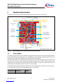
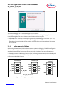
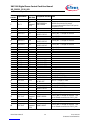
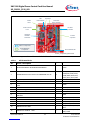
Infineon Technologies XMC1300 is a 32-bit microcontroller series designed for industrial applications. It features an ARM Cortex-M0 core, up to 200 KB of flash memory, and a variety of peripherals, including a 12-bit ADC, two CCU8 cores, and a USIC channel. The XMC1300 is ideal for applications such as motor control, power supplies, and lighting. It is also supported by the DAVE development environment, which makes it easy to develop and debug applications.
Infineon Technologies XMC1300 is a 32-bit microcontroller series designed for industrial applications. It features an ARM Cortex-M0 core, up to 200 KB of flash memory, and a variety of peripherals, including a 12-bit ADC, two CCU8 cores, and a USIC channel. The XMC1300 is ideal for applications such as motor control, power supplies, and lighting. It is also supported by the DAVE development environment, which makes it easy to develop and debug applications.


-
 1
1
-
 2
2
-
 3
3
-
 4
4
-
 5
5
-
 6
6
-
 7
7
-
 8
8
-
 9
9
-
 10
10
-
 11
11
-
 12
12
-
 13
13
-
 14
14
-
 15
15
-
 16
16
-
 17
17
-
 18
18
-
 19
19
-
 20
20
-
 21
21
-
 22
22
-
 23
23
-
 24
24


Infineon Technologies XMC1300 User manual
- Type
- User manual
Infineon Technologies XMC1300 is a 32-bit microcontroller series designed for industrial applications. It features an ARM Cortex-M0 core, up to 200 KB of flash memory, and a variety of peripherals, including a 12-bit ADC, two CCU8 cores, and a USIC channel. The XMC1300 is ideal for applications such as motor control, power supplies, and lighting. It is also supported by the DAVE development environment, which makes it easy to develop and debug applications.
Ask a question and I''ll find the answer in the document
Finding information in a document is now easier with AI
Related papers

Other documents
-
Infineon KIT_XMC750WATT_MC_AK_V1 Operating instructions
-
-
Infineon XMC4502-F100F768 AC User manual
-
Silicon Labs UG239 User guide
-
-
-
-
-
-