Intel HDMI PHY User guide

Type
User guide

Intel HDMI PHY is a high-performance, low-power solution that enables reliable and secure transmission of uncompressed high-definition video and audio signals over long distances. It supports the latest HDMI 2.0 standard, featuring data rates up to 6 Gbps, 4K Ultra HD video resolution, and High Dynamic Range (HDR) for vibrant, lifelike visuals. With its advanced features and capabilities, Intel HDMI PHY is ideal for a wide range of applications, including home entertainment systems, digital signage, video conferencing, and more.

Intel HDMI PHY is a high-performance, low-power solution that enables reliable and secure transmission of uncompressed high-definition video and audio signals over long distances. It supports the latest HDMI 2.0 standard, featuring data rates up to 6 Gbps, 4K Ultra HD video resolution, and High Dynamic Range (HDR) for vibrant, lifelike visuals. With its advanced features and capabilities, Intel HDMI PHY is ideal for a wide range of applications, including home entertainment systems, digital signage, video conferencing, and more.

HDMI PHY Intel FPGA IP Design
Example User Guide
Updated for Intel® Quartus® Prime Design Suite: 22.2
IP Version: 1.0.0
Online Version
Send Feedback
ID: 732781
Version: 2022.07.20
Contents
1. HDMI PHY Design Example Quick Start Guide for Intel® Arria® 10 Devices.....................3
1.1. Generating the Design............................................................................................3
1.2. Compiling and Testing the Design............................................................................ 4
1.3. HDMI PHY Intel FPGA IP Design Example Parameters..................................................5
2. HDMI 2.0 PHY Design Example....................................................................................... 6
2.1. Hardware and Software Requirements...................................................................... 7
2.1.1. Hardware................................................................................................. 7
2.1.2. Software.................................................................................................. 7
2.2. Directory Structure................................................................................................ 7
2.3. Reconfiguration Sequence Flow................................................................................9
2.4. Interface Signals..................................................................................................10
2.5. Clocking Scheme................................................................................................. 11
2.6. Hardware Setup...................................................................................................11
3. Document Revision History for the HDMI PHY Intel FPGA IP Design Example User
Guide....................................................................................................................... 13
Contents
HDMI PHY Intel FPGA IP Design Example User Guide Send Feedback
2
1. HDMI PHY Design Example Quick Start Guide for Intel®
Arria® 10 Devices
The HDMI PHY Intel® FPGA IP design example for Intel Arria® 10 devices features a
HDMI 2.0 RX-TX retransmit design that supports compilation and hardware testing.
When you generate a design example, the parameter editor automatically creates the
files necessary to simulate, compile, and test the design in hardware.
Figure 1. Development Steps
Design
Example
Generation
Compilation
(Simulator)
Functional
Simulation
Compilation
(Quartus Prime)
Hardware
Testing
Related Information
HDMI PHY Intel FPGA IP User Guide
1.1. Generating the Design
Use the HDMI PHY Intel FPGA IP parameter editor in the Intel Quartus® Prime
software to generate the design examples.
Figure 2. Generating the Design Flow
Start Parameter
Editor
Specify IP Variation
and Select Device
Select
Design Parameters
Initiate
Design Generation
Specify
Example Design
1. Create a project targeting Intel Arria 10 device family and select the desired
device.
2. In the IP Catalog, locate and double-click Interface Protocols Audio & Video
HDMI TX PHY Intel FPGA IP (or HDMI RX PHY Intel FPGA IP). The New
IP Variant or New IP Variation window appears.
3. Specify a top-level name for your custom IP variation. The parameter editor saves
the IP variation settings in a file named <your_ip>.ip or <your_ip>.qsys.
4. Click OK. The parameter editor appears.
732781 | 2022.07.20
Send Feedback
Intel Corporation. All rights reserved. Intel, the Intel logo, and other Intel marks are trademarks of Intel
Corporation or its subsidiaries. Intel warrants performance of its FPGA and semiconductor products to current
specifications in accordance with Intel's standard warranty, but reserves the right to make changes to any
products and services at any time without notice. Intel assumes no responsibility or liability arising out of the
application or use of any information, product, or service described herein except as expressly agreed to in
writing by Intel. Intel customers are advised to obtain the latest version of device specifications before relying
on any published information and before placing orders for products or services.
*Other names and brands may be claimed as the property of others.
ISO
9001:2015
Registered
5. On the Design Example tab, select Arria 10 HDMI RX-TX Retransmit.
6. Select Simulation to generate the testbench, and select Synthesis to generate
the hardware design example.
You must select at least one of these options to generate the design example files.
If you select both, the generation time is longer.
7. For Generate File Format, select Verilog or VHDL.
8. For Target Development Kit, select Intel Arria 10 GX FPGA Development
Kit. If you select a development kit, then the target device changes to match the
device on target board. For Intel Arria 10 GX FPGA Development Kit, the
default device is 10AX115S2F4I1SG.
9. Click Generate Example Design.
1.2. Compiling and Testing the Design
Compile Design
in Quartus Prime
Software
Set Up Hardware Program Device Test Design
in Hardware
To compile and run a demonstration test on the hardware example design, follow
these steps:
1. Ensure hardware example design generation is complete.
2. Launch the Intel Quartus Prime software and open the .qpf file: <Design
Example>/quartus/a10_hdmi2_demo.qpf
3. Click Processing Start Compilation.
4. After successful compilation, a .sof file is generated in the quartus/
output_files directory.
5. Connect Bitec HDMI 2.0 FMC Daughter Card Rev 11 to the on-board FMC port B
(J2).
6. Connect TX (P1) of the Bitec FMC daughter card to an external video source.
7. Connect RX (P2) of the Bitec FMC daughter card to an external video sink or video
analyzer.
8. Ensure all switches on the development board are in default position.
9. Configure the selected Intel Arria 10 device on the development board using the
generated .sof file (Tools Programmer).
10. The analyzer should display the video generated from the source.
Related Information
Intel Arria 10 FPGA Development Kit User Guide
1. HDMI PHY Design Example Quick Start Guide for Intel® Arria® 10 Devices
732781 | 2022.07.20
HDMI PHY Intel FPGA IP Design Example User Guide Send Feedback
4
1.3. HDMI PHY Intel FPGA IP Design Example Parameters
Table 1. HDMI PHY Intel FPGA IP Design Example Parameters for Intel Arria 10
Devices
These options are available for Intel Arria 10 devices only.
Parameter Value Description
Available Design Example
Select Design Arria 10 HDMI RX-TX
Retransmit
Select the design example to be generated.
Design Example Files
Simulation On, Off Turn on this option to generate the necessary files for the simulation
testbench.
Synthesis On, Off Turn on this option to generate the necessary files for Intel Quartus
Prime compilation and hardware demonstration.
Generated HDL Format
Generate File Format Verilog, VHDL Select your preferred HDL format for the generated design example
fileset.
Note: This option only determines the format for the generated top
level IP files. All other files (e.g., example testbenches and top
level files for hardware demonstration) are in Verilog HDL format.
Target Development Kit
Select Board No Development Kit,
Arria 10 GX FPGA
Development Kit,
Custom Development
Kit
Select the board for the targeted design example.
No Development Kit: This option excludes all hardware aspects for
the design example. The IP core sets all pin assignments to virtual
pins.
Arria 10 GX FPGA Development Kit: This option automatically selects
the project's target device to match the device on this development
kit. You may change the target device using the Change Target
Device parameter if your board revision has a different device
variant. The IP core sets all pin assignments according to the
development kit.
Custom Development Kit: This option allows the design example to
be tested on a third party development kit with an Intel FPGA. You
may need to set the pin assignments on your own.
Target Device
Change Target Device On, Off Turn on this option and select the preferred device variant for the
development kit.
Related Information
Intel Arria 10 FPGA Development Kit User Guide
1. HDMI PHY Design Example Quick Start Guide for Intel® Arria® 10 Devices
732781 | 2022.07.20
Send Feedback HDMI PHY Intel FPGA IP Design Example User Guide
5
2. HDMI 2.0 PHY Design Example
The HDMI PHY Intel FPGA IP design example demonstrates one HDMI instance parallel
loopback comprising three RX channels and four TX channels, operating at data rates
up to 6 Gbps.
The generated HDMI PHY Intel FPGA IP design example is the same as the design
example generated in the HDMI Intel FPGA IP core. However, this design example
uses the new TX PHY, RX PHY, and PHY arbiter instead of custom RTL in the HDMI Intel
FPGA IP core design example.
Figure 3. HDMI 2.0 PHY Design Example
IOPLL
AXI Stream Clock mgmt_clk
TX_clk
AXI_Stream_Clock
RX_CLK[2:0]
AXI4-Stream
Video
rxphy_rcfg_master
txphy_rcfg_master txphy_rcfg_slave
rxphy_rcfg_slave
PHY Interface
PHY Interface Serial RX
Serial TX
I2C to PCB
Components
TX PHY
PHY Arbiter I2C
Master
HDMI TX
Core
RX PHY
HDMI RX
Core
Table 2. HDMI PHY Components
Module Description
RX PHY The RX PHY recovers serial HDMI data and send this to the
HDMI RX core in parallel format on the recovered clock
domains (rx_clk[2:0]). The data is decoded into video
continued...
732781 | 2022.07.20
Send Feedback
Intel Corporation. All rights reserved. Intel, the Intel logo, and other Intel marks are trademarks of Intel
Corporation or its subsidiaries. Intel warrants performance of its FPGA and semiconductor products to current
specifications in accordance with Intel's standard warranty, but reserves the right to make changes to any
products and services at any time without notice. Intel assumes no responsibility or liability arising out of the
application or use of any information, product, or service described herein except as expressly agreed to in
writing by Intel. Intel customers are advised to obtain the latest version of device specifications before relying
on any published information and before placing orders for products or services.
*Other names and brands may be claimed as the property of others.
ISO
9001:2015
Registered
Module Description
data to be output via AXI4-stream video. The RX PHY also
sends vid_clk and ls_clk signals to the HDMI RX core
via the PHY interface.
HDMI TX Core The HDMI TX core receives AXI4-stream video data and
encodes this into HDMI format parallel data. The HDMI TX
core sends this data to the TX PHY.
HDMI RX Core The IP receives the serial data from the RX PHY and
performs data alignment, channel deskew, TMDS decoding,
auxiliary data decoding, video data decoding, audio data
decoding, and descrambling.
TX PHY Receives and serializes the parallel data from the HDMI TX
core and outputs HDMI TMDS streams. The TX PHY
produces tx_clk for the HDMI TX core. The TX PHY also
generates vid_clk and ls_clk and sends these signals to
the HDMI TX core via the PHY interface.
IOPLL Generates 300 MHz AXI serial stream clock for the AXI4-
stream interface.
I2C Master To configure the various PCB components.
2.1. Hardware and Software Requirements
Intel uses the following hardware and software to test the design example.
2.1.1. Hardware
Intel Arria 10 GX FPGA Development Kit
HDMI Source (Graphics Processor Unit (GPU)
HDMI Sink (Monitor)
Bitec HDMI FMC 2.0 daughter card (Revision 11)
HDMI cables
2.1.2. Software
Intel Quartus Prime Pro Edition (for hardware testing)
ModelSim* - Intel FPGA Edition, ModelSim - Intel FPGA Starter Edition, NCSim,
Riviera-PRO*, VCS* (Verilog HDL only)/VCS MX, or Xcelium* Parallel simulator
2.2. Directory Structure
The directories contain the generated file for the HDMI Intel FPGA IP design example.
2. HDMI 2.0 PHY Design Example
732781 | 2022.07.20
Send Feedback HDMI PHY Intel FPGA IP Design Example User Guide
7
Figure 4. Directory Structure for the Design Example
<Design Example>
Pro = Intel Quartus Prime Pro Edition
Std = Intel Quartus Prime Standard Edition
quartus
db (Standard)/qdb (Pro)
a10_hdmi2_demo.qpf
a10_hdmi2_demo.qsf
rtl
nios.qsys
jtag.sdc
Panasonic.hex
a10_hdmi2_demo.v
script
build_sw.sh
intel_hdmi_common
intel_hdmi_rx_core
intel_hdmi_rx_phy
intel_hdmi_tx_core
intel_hdmi_tx_phy
src
software
2. HDMI 2.0 PHY Design Example
732781 | 2022.07.20
HDMI PHY Intel FPGA IP Design Example User Guide Send Feedback
8
2.3. Reconfiguration Sequence Flow
Figure 5. Multi-rate Reconfiguration Sequence Flow
The figure illustrates the multi-rate reconfiguration sequence flow of the controller when it receives input data
stream and reference clock frequency, or when the transceiver is unlocked.
Reset the RX HDMI PLL and RX transceiver.
Enable the rate detection circuit to measure incoming TMDS clock.
Reconfiguration Required
Reconfiguration
Not Required
Determine if RX HDMI PLL and/or RX transceiver reconfiguration
is required based on the previous and current detected clock
frequency band and color depth. Different color depths may fall
within the same clock frequency band.
When all reconfiguration processes complete or the previous
and current clock frequency band and color depth do not differ,
reset the RX HDMI PLL and RX transceiver.
Request RX HDMI PLL and/or RX transceiver reconfiguration if the
previous and current clock frequency band or color depth differs.
Accept acknowledgement with clock frequency band and desired
RX HDMI PLL and RX transceiver settings.
The controller reconfigures the RX HDMI PLL and/or RX transceiver
(followed by recalibration on the Intel FPGA device).
Enable rate the detection circuit periodically to monitor the
reference clock frequency. If the clock frequency band changes
or the RX HDMI PLL or RX transceiver or HDMI core loses lock,
repeat the process.
2. HDMI 2.0 PHY Design Example
732781 | 2022.07.20
Send Feedback HDMI PHY Intel FPGA IP Design Example User Guide
9
Figure 6. Reconfiguration Sequence Flow
The figure illustrates the Nios II software flow that involves the controls for I2C master and HDMI TX PHY.
Reset the TX HDMI PLL and TX transceiver. Initialize the I2C Master Controller Core.
Read TMDS_bit_clock_ratio value from
the HDMI sink and measure value.
Measure Valid Received A TX Hot-Plug Event Occurred
Poll periodic measure valid signal from RX data detection circuit to determine
whether TX reconfiguration is required. Also, poll the TX hot-plug request to
determine whether a TX hot-plug event has occurred.
Retrieve the clock frequency band based on
the measure and TMDS_bit_clock_ratio
values and read the color depth information
from the HDMI sink to determine whether
TX HDMI PLL and TX transceiver reconfigu-
ration and oversampling is required.
The Nios II processor commands the I2C
master to send SCDC information.
Nios II processor sends sequential commands
to reconfigure the TX HDMI PLL and TX
transceiver (followed by recalibration on the
Intel FPGA device), and reset sequence after
reconfiguration. It then sends a reset to
the HDMI TX core.
Deassert edid_ram_access control signal
to enable the HDMI RX Top to trigger a
hotplug detect event to the external
HDMI source.
Read EDID from external sink through I2C
interface and write the EDID content to
the HDMI RX EDID RAM.
Assert HDMI RX Top’s edid_ram_access
control signal to block HDMI sink’s EDID
RAM from being accessed by external
HDMI source.
Send TMDS_bit_clock_ratio and
scrambler_enable information to the
external HDMI sink’s SCDC registers
through the I2C interface.
Reconfiguration
Not Required
Reconfiguration Required
2.4. Interface Signals
The tables list the signals for the HDMI PHY Intel FPGA IP design example.
Table 3. Top-Level Signals
Signal Direction Width Description
On-board Oscillator Signal
clk_fpga_b3_p Input 1 100 MHz free running clock for core
reference clock
refclk_fmcb_p Input 1 Fixed rate reference clock for power-up
calibration of the transceiver. It is 625
MHz by default but can be of any
frequency
2. HDMI 2.0 PHY Design Example
732781 | 2022.07.20
HDMI PHY Intel FPGA IP Design Example User Guide Send Feedback
10
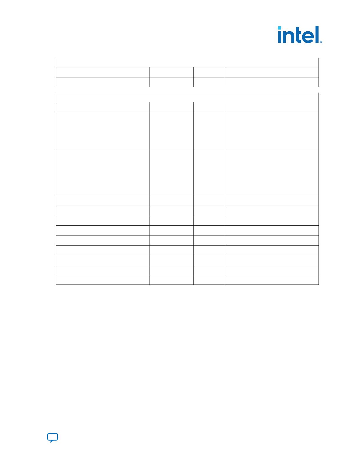
User Push Buttons and LEDs
cpu_resetn Input 1 Global reset
user_led_g Output 2 Green LED display
HDMI FMC Daughter Card Pins on FMC Port B
fmcb_gbtclk_m2c_p_0 Input 1 HDMI RX TMDS clock
fmcb_dp_m2c_p Input 3 HDMI RX red, green, and blue data
channels
Bitec daughter card revision 11
[0]: RX TMDS Channel 1 (Green)
[1]: RX TMDS Channel 2 (Red)
[2]: RX TMDS Channel 0 (Blue)
fmcb_dp_c2m_p Output 4 HDMI TX clock, red, green, and blue data
channels
Bitec daughter card revision 11
[0]: TX TMDS Channel 2 (Red)
[1]: TX TMDS Channel 1 (Green)
[2]: TX TMDS Channel 0 (Blue)
[3]: TX TMDS Clock Channel
fmcb_la_rx_p_9 Input 1 HDMI RX +5V power detect
fmcb_la_rx_p_8 Input 1 HDMI RX hot plug detect
fmcb_la_rx_n_8 Input 1 HDMI RX I2C SDA for DDC and SCDC
fmcb_la_tx_p_10 Input 1 HDMI RX I2C SCL for DDC and SCDC
fmcb_la_tx_p_12 Input 1 HDMI TX hot plug detect
fmcb_la_tx_n_12 Input 1 HDMI I2C SDA for DDC and SCDC
fmcb_la_rx_p_10 Input 1 HDMI I2C SCL for DDC and SCDC
fmcb_la_tx_p_11 Input 1 HDMI I2C SDA for redriver control
fmcb_la_rx_n_9 Input 1 HDMI I2C SCL for redriver control
2.5. Clocking Scheme
The following is the clocking scheme of the HDMI PHY Intel FPGA IP design example:
clk_fpga_b3_p is a 100 MHz fixed rate clock for running the NIOS processor and
control functions. If the supplied frequency is correct, the user_led_g[1]
toggles for every second.
refclk_fmcb_p is a fixed rate reference clock for power-up calibration of the
transceivers. It is 625 MHz by default but can be of any frequency.
fmcb_gbtclk_m2c_p_0 is the TMDS clock for HDMI RX. This clock is also used to
drive the HDMI TX transceivers. If the supplied frequency is 148.5 MHz, the
user_led_g[0] toggles for every second.
2.6. Hardware Setup
The HDMI PHY Intel FPGA IP design example is HDMI 2.0b capable and performs a
loop-through demonstration for a standard HDMI video stream.
2. HDMI 2.0 PHY Design Example
732781 | 2022.07.20
Send Feedback HDMI PHY Intel FPGA IP Design Example User Guide
11
To run the hardware test, connect an HDMI-enabled device such as a graphics card
with HDMI interface to the HDMI RX connector on the Bitec HDMI 2.0 daughter card,
which route the data to the transceiver RX block and HDMI RX.
1. The HDMI sink decodes the port into a standard video stream and sends it to the
clock recovery core.
2. The HDMI RX core decodes the video, auxiliary, and audio data to be looped back
via AXI4-stream interface to the HDMI TX core.
3. The HDMI source port of the FMC daughter card transmits the image to a monitor.
4. Press the cpu_resetn button once to perform system reset.
Note: If you want to use another Intel FPGA development board, you must change the
device assignments and the pin assignments. The transceiver analog setting is tested
for the Intel Arria 10 FPGA development kit and Bitec HDMI 2.0 daughter card. You
may modify the settings for your own board.
2. HDMI 2.0 PHY Design Example
732781 | 2022.07.20
HDMI PHY Intel FPGA IP Design Example User Guide Send Feedback
12
3. Document Revision History for the HDMI PHY Intel
FPGA IP Design Example User Guide
Document Version Intel Quartus
Prime Version
IP Version Changes
2022.07.20 22.2 1.0.0 Initial release.
732781 | 2022.07.20
Send Feedback
Intel Corporation. All rights reserved. Intel, the Intel logo, and other Intel marks are trademarks of Intel
Corporation or its subsidiaries. Intel warrants performance of its FPGA and semiconductor products to current
specifications in accordance with Intel's standard warranty, but reserves the right to make changes to any
products and services at any time without notice. Intel assumes no responsibility or liability arising out of the
application or use of any information, product, or service described herein except as expressly agreed to in
writing by Intel. Intel customers are advised to obtain the latest version of device specifications before relying
on any published information and before placing orders for products or services.
*Other names and brands may be claimed as the property of others.
ISO
9001:2015
Registered
  • Page 1 1
  • Page 2 2
  • Page 3 3
  • Page 4 4
  • Page 5 5
  • Page 6 6
  • Page 7 7
  • Page 8 8
  • Page 9 9
  • Page 10 10
  • Page 11 11
  • Page 12 12
  • Page 13 13

Intel HDMI PHY User guide

Type
User guide

Intel HDMI PHY is a high-performance, low-power solution that enables reliable and secure transmission of uncompressed high-definition video and audio signals over long distances. It supports the latest HDMI 2.0 standard, featuring data rates up to 6 Gbps, 4K Ultra HD video resolution, and High Dynamic Range (HDR) for vibrant, lifelike visuals. With its advanced features and capabilities, Intel HDMI PHY is ideal for a wide range of applications, including home entertainment systems, digital signage, video conferencing, and more.

Ask a question and I''ll find the answer in the document

Finding information in a document is now easier with AI