Page is loading ...


2 CY8CKIT-050 PSoC® 5LP Development Kit Guide, Doc. # 001-65816 Rev. *E
Copyrights
Copyrights
© Cypress Semiconductor Corporation, 2011-2012. The information contained herein is subject to change without notice.
Cypress Semiconductor Corporation assumes no responsibility for the use of any circuitry other than circuitry embodied in a
Cypress product. Nor does it convey or imply any license under patent or other rights. Cypress products are not warranted
nor intended to be used for medical, life support, life saving, critical control or safety applications, unless pursuant to an
express written agreement with Cypress. Furthermore, Cypress does not authorize its products for use as critical components
in life-support systems where a malfunction or failure may reasonably be expected to result in significant injury to the user.
The inclusion of Cypress products in life-support systems application implies that the manufacturer assumes all risk of such
use and in doing so indemnifies Cypress against all charges.
Any Source Code (software and/or firmware) is owned by Cypress Semiconductor Corporation (Cypress) and is protected by
and subject to worldwide patent protection (United States and foreign), United States copyright laws and international treaty
provisions. Cypress hereby grants to licensee a personal, non-exclusive, non-transferable license to copy, use, modify, create
derivative works of, and compile the Cypress Source Code and derivative works for the sole purpose of creating custom soft-
ware and or firmware in support of licensee product to be used only in conjunction with a Cypress integrated circuit as speci-
fied in the applicable agreement. Any reproduction, modification, translation, compilation, or representation of this Source
Code except as specified above is prohibited without the express written permission of Cypress.
Disclaimer: CYPRESS MAKES NO WARRANTY OF ANY KIND, EXPRESS OR IMPLIED, WITH REGARD TO THIS MATE-
RIAL, INCLUDING, BUT NOT LIMITED TO, THE IMPLIED WARRANTIES OF MERCHANTABILITY AND FITNESS FOR A
PARTICULAR PURPOSE. Cypress reserves the right to make changes without further notice to the materials described
herein. Cypress does not assume any liability arising out of the application or use of any product or circuit described herein.
Cypress does not authorize its products for use as critical components in life-support systems where a malfunction or failure
may reasonably be expected to result in significant injury to the user. The inclusion of Cypress’ product in a life-support sys-
tems application implies that the manufacturer assumes all risk of such use and in doing so indemnifies Cypress against all
charges.
Use may be limited by and subject to the applicable Cypress software license agreement.
PSoC Creator™ is a trademark, and PSoC® and CapSense® are registered trademarks of Cypress Semiconductor Corp. All
other trademarks or registered trademarks referenced herein are property of the respective corporations.
Flash Code Protection
Cypress products meet the specifications contained in their particular Cypress PSoC Data Sheets. Cypress believes that its
family of PSoC products is one of the most secure families of its kind on the market today, regardless of how they are used.
There may be methods, unknown to Cypress, that can breach the code protection features. Any of these methods, to our
knowledge, would be dishonest and possibly illegal. Neither Cypress nor any other semiconductor manufacturer can guaran-
tee the security of their code. Code protection does not mean that we are guaranteeing the product as ‘unbreakable’.
Cypress is willing to work with the customer who is concerned about the integrity of their code. Code protection is constantly
evolving. We at Cypress are committed to continuously improving the code protection features of our products.

CY8CKIT-050 PSoC® 5LP Development Kit Guide, Doc. # 001-65816 Rev. *E 3
Contents
1. Introduction 5
1.1 Kit Contents.................................................................................................................5
1.2 PSoC Creator ..............................................................................................................5
1.3 Additional Learning Resources....................................................................................6
1.3.1 Beginner Resources.........................................................................................6
1.3.2 Engineers Looking for More.............................................................................6
1.3.3 Learn from Peers .............................................................................................6
1.3.4 More Code Examples.......................................................................................6
1.4 Document History ........................................................................................................9
1.5 Documentation Conventions .......................................................................................9
2. Getting Started 11
2.1 Introduction................................................................................................................11
2.2 CD Installation ...........................................................................................................11
2.3 Install Hardware.........................................................................................................12
2.4 Install Software ..........................................................................................................12
2.5 Uninstall Software......................................................................................................12
2.6 Verify Kit Version .......................................................................................................12
3. Kit Operation 13
3.1 Programming PSoC 5LP Device ...............................................................................13
4. Hardware 17
4.1 System Block Diagram ..............................................................................................17
4.2 Functional Description ...............................................................................................18
4.2.1 Power Supply.................................................................................................18
4.2.1.1 Power Supply Jumper Settings........................................................19
4.2.1.2 Grounding Scheme..........................................................................20
4.2.1.3 Low-Power Functionality..................................................................20
4.2.1.4 AC/DC Adaptor Specifications.........................................................21
4.2.1.5 Battery Specifications ......................................................................21
4.2.2 Programming Interface...................................................................................21
4.2.2.1 On-board Programming Interface....................................................21
4.2.2.2 JTAG/SWD Programming................................................................22
4.2.3 USB Communication......................................................................................23
4.2.4 Boost Convertor.............................................................................................23
4.2.5 32-kHz and 24-MHz Crystal...........................................................................24
4.2.6 Protection Circuit............................................................................................24
4.2.6.1 Functional Description of Circuit......................................................25
4.2.7 PSoC 5LP Development Kit Expansion Ports................................................26
4.2.7.1 Port D...............................................................................................26
4.2.7.2 Port E...............................................................................................28

4 CY8CKIT-050 PSoC® 5LP Development Kit Guide, Doc. # 001-65816 Rev. *E
Contents
4.2.8 RS-232 Interface............................................................................................29
4.2.9 Prototyping Area............................................................................................29
4.2.10 Character LCD...............................................................................................30
4.2.11 CapSense Sensors........................................................................................31
5. Code Examples 33
5.1 Project: VoltageDisplay_SAR_ADC ..........................................................................34
5.1.1 Project Description.........................................................................................34
5.1.2 Hardware Connections ..................................................................................34
5.1.3 SAR ADC Configuration.................................................................................34
5.1.4 Verify Output..................................................................................................35
5.2 Project: VoltageDisplay_DelSigADC.........................................................................35
5.2.1 Project Description.........................................................................................35
5.2.2 Hardware Connections ..................................................................................36
5.2.3 Del-Sig ADC Configuration............................................................................36
5.2.4 Verify Output..................................................................................................37
5.3 Project: IntensityLED.................................................................................................38
5.3.1 Project Description.........................................................................................38
5.3.2 Hardware Connections ..................................................................................38
5.3.3 Verify Output..................................................................................................38
5.4 Project: LowPowerDemo...........................................................................................38
5.4.1 Project Description.........................................................................................38
5.4.2 Hardware Connections ..................................................................................38
5.4.3 Verify Output..................................................................................................39
5.5 Project: CapSense.....................................................................................................39
5.5.1 Project Description.........................................................................................39
5.5.2 Hardware Connections ..................................................................................40
5.5.3 Verify Output..................................................................................................40
5.6 Project: ADC_DAC....................................................................................................41
5.6.1 Project Description.........................................................................................41
5.6.2 Hardware Connections ..................................................................................41
5.6.3 Verify Output..................................................................................................41
A. Appendix 43
A.1 Schematic..................................................................................................................43
A.2 Board Layout.............................................................................................................49
A.2.1 PDC-09356 Top.............................................................................................49
A.2.2 PDC-09356 Power.........................................................................................50
A.2.3 PDC-09356 Ground.......................................................................................51
A.2.4 PDC-09356 Bottom........................................................................................52
A.3 Bill of Materials (BOM)...............................................................................................53
A.4 Pin Assignment Table................................................................................................58

CY8CKIT-050 PSoC® 5LP Development Kit Guide, Doc. # 001-65816 Rev. *E 5
1. Introduction
Thank you for your interest in the CY8CKIT-050 PSoC® 5 Development Kit. This kit allows you to
develop precision analog and low-power designs using PSoC 5LP. You can design your own projects
with PSoC Creator™ or alter the sample projects provided with this kit.
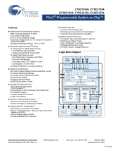
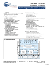
The CY8CKIT-050 PSoC 5LP Development Kit is based on the PSoC 5LP family of devices.
PSoC 5LP is a Programmable System-on-Chip™ platform for 8-bit, 16-bit, and 32-bit applications. It
combines precision analog and digital logic with a high-performance CPU. With PSoC, you can
create the exact combination of peripherals and integrated proprietary IP to meet your application
requirements.
1.1 Kit Contents
The PSoC 5LP Development Kit contains:
■Development board
■Kit CD
■Quick start guide
■USB A to mini B cable
■3.3 V LCD module
Inspect the contents of the kit; if you find any part missing, contact your nearest Cypress sales office
for help.
1.2 PSoC Creator
Cypress's PSoC Creator software is a state-of-the-art, easy-to-use integrated development
environment (IDE) that introduces a hardware and software design environment based on classic
schematic entry and revolutionary embedded design methodology.
With PSoC Creator, you can:
■Create and share user-defined, custom peripherals using hierarchical schematic design.
■Automatically place and route select components and integrate simple glue logic, normally
located in discrete muxes.
■Trade off hardware and software design considerations allowing you to focus on what matters
and getting to market faster.
PSoC Creator also enables you to tap into an entire tools ecosystem with integrated compiler tool
chains, RTOS solutions, and production programmers to support both PSoC 3 and PSoC 5LP.

6 CY8CKIT-050 PSoC® 5LP Development Kit Guide, Doc. # 001-65816 Rev. *E
Introduction
1.3 Additional Learning Resources
Visit http://www.cypress.com/go/psoc5 for additional learning resources in the form of datasheets,
technical reference manual, and application notes.
1.3.1 Beginner Resources
AN77759 - Getting Started with PSoC 5
PSoC Creator Training
1.3.2 Engineers Looking for More
AN54460 - PSoC 3 and PSoC 5 Interrupts
AN52705 - PSoC 3 and PSoC 5 - Getting Started with DMA
AN52701 - PSoC 3 - How to Enable CAN Bus Communication
AN54439 - PSoC 3 and PSoC 5 External Crystal Oscillators
AN52927 - PSoC 3: Segment LCD Direct Drive
Cypress continually strives to provide the best support. Click here to view a growing list of
application notes for PSoC 3 and PSoC 5LP.
1.3.3 Learn from Peers
Cypress Developer Community Forums
1.3.4 More Code Examples
PSoC Creator provides a host of example projects that makes the code development very fast and
easy. To access these example projects, click on the Find Example Project… under Example and
Kits section in Start Page of PSoC Creator or by navigating to File->Open-Example Project…

CY8CKIT-050 PSoC® 5LP Development Kit Guide, Doc. # 001-65816 Rev. *E 7
Introduction
The Find Example project has various filters that help you locate the most relevant project you are
looking for.
PSoC Creator provides several Starter Designs. These designs highlight features that are unique to
PSoC devices. They allow you to create a design with various components and code is also pro-
vided, instead of creating a new empty design. To use a starter design for your project, navigate to
File->New->Project and select the design required.

8 CY8CKIT-050 PSoC® 5LP Development Kit Guide, Doc. # 001-65816 Rev. *E
Introduction
The example projects and starter designs are designed for CY8CKIT-001 PSoC Development Kit.
However, these projects can be converted for use with CY8CKIT-030 PSoC 3 Development Kit or
CY8CKIT-050 PSoC 5 Development Kit by following the procedure in the knowledge base article
Migrating project from CY8CKIT-001 to CY8CKIT-030 or CY8CKIT-050.
Apart from the example projects and starter designs that are available within PSoC Creator, Cypress
continuously strives to provide the best support. Click here to view a growing list of application notes
for PSoC 3 and PSoC 5.

CY8CKIT-050 PSoC® 5LP Development Kit Guide, Doc. # 001-65816 Rev. *E 9
Introduction
1.4 Document History
1.5 Documentation Conventions
Revision PDF Creation
Date Origin of
Change Description of Change
** 03/01/2011 PVKV Initial version of kit guide
*A 04/28/2011 RKAD Updated Schematic
*B 12/15/2011 RKAD Added sections 4.2.1.4 and 4.2.1.5. Added Pin Assignment table in
the Appendix. Updated bill of materials. Content updates throughout
the document
*C 05/15/2012 SASH Updated the Additional Resources section
*D 06/18/2012 SASH Updated CD Installation on page 11.
*E 11/08/2012 SASH Updated images
Table 1-1. Document Conventions for Guides
Convention Usage
Courier New Displays file locations, user entered text, and source code:
C:\ ...cd\icc\
Italics Displays file names and reference documentation:
Read about the sourcefile.hex file in the PSoC Designer User Guide.
[Bracketed, Bold]Displays keyboard commands in procedures:
[Enter] or [Ctrl] [C]
File > Open Represents menu paths:
File > Open > New Project
Bold Displays commands, menu paths, and icon names in procedures:
Click the File icon and then click Open.
Times New Roman Displays an equation:
2 + 2 = 4
Text in gray boxes Describes cautions or unique functionality of the product.


CY8CKIT-050 PSoC® 5LP Development Kit Guide, Doc. # 001-65816 Rev. *E 11
2. Getting Started
2.1 Introduction
This chapter describes how to install and configure the PSoC 5LP Development Kit. Chapter 3
describes the kit operation. It explains how to program a PSoC 5LP device with PSoC Programmer
and use the kit with the help of a code example. To reprogram the PSoC device with PSoC Creator,
see the CD installation instructions for PSoC Creator. Chapter 4 details the hardware operation.
Chapter 5 provides instructions to create a simple code example. The Appendix section provides the
schematics and bill of materials associated with the PSoC 5LP Development Kit.
2.2 CD Installation
Follow these steps to install the PSoC 5LP Development Kit software:
1. Insert the kit CD into the CD drive of your PC. The CD is designed to auto-run and the kit menu
appears.
Figure 2-1. Kit Menu
Note If auto-run does not execute, double-click cyautorun.exe on the root directory of the CD.

12 CY8CKIT-050 PSoC® 5LP Development Kit Guide, Doc. # 001-65816 Rev. *E
Getting Started
After the installation is complete, the kit contents are available at the following location:
<Install_Directory>:\PSoC 5LP Development Kit\<version>
2.3 Install Hardware
No hardware installation is required for this kit.
2.4 Install Software
When installing the PSoC 5LP Development Kit, the installer checks if your system has the required
software. These include PSoC Creator, PSoC Programmer, Windows Installer, .NET, Acrobat
Reader, and KEIL Complier. If these applications are not installed, the installer prompts you to down-
load and install them.
Install the following software from the kit CD:
■PSoC Creator
■PSoC Programmer 3.16 or later
Note When installing PSoC Programmer, select Typical on the Installation Type page.
■Code examples (provided in the Firmware folder)
2.5 Uninstall Software
The software can be uninstalled using one of the following methods:
■Go to Start > Control Panel > Add or Remove Programs; select the Remove button.
■Go to Start > All Programs > Cypress > Cypress Update Manager > Cypress Update Man-
ager; select the Uninstall button.
■Insert the installation CD and click Install PSoC 5LP Development Kit button. In the CyInstaller
for PSoC 5LP Development Kit 2.1 window, select Remove from the Installation Type drop-
down menu. Follow the instructions to uninstall.
2.6 Verify Kit Version
To know the kit revision, look for the white sticker on the bottom left, on the reverse of the kit box. If
the revision reads CY8CKIT-050B Rev **, then, you own the latest version.
To upgrade CY8CKIT-050/CY8CKIT-050A to CY8CKIT-050B, you can purchase our latest kits at
http://www.cypress.com/go/CY8CKIT-050.

CY8CKIT-050 PSoC® 5LP Development Kit Guide, Doc. # 001-65816 Rev. *E 13
3. Kit Operation
The code examples in the PSoC 5LP Development Kit help you develop applications using the
PSoC 5LP family of devices. The kit is designed to develop precision analog applications using
PSoC 5LP. The board also has hooks to enable low-power measurements for low-power application
development and evaluation.
3.1 Programming PSoC 5LP Device
The default programming interface for the board is a USB-based on-board programming interface.
To program the device, plug the USB cable to the programming USB connector J1, as shown in the
following figure.
Figure 3-1. Connect USB Cable to J1
When plugged in, the board enumerates as DVKProg5. After enumeration, initiate, build, and then
program using PSoC Creator.
When using on-board programming, it is not necessary to power the board from the 12-V or 9-V DC
supply or a battery. The USB power to the programming section can be used.
If the board is already powered from another source, plugging in the programming USB does not
damage the board.
The PSoC 5LP device on the board can also be programmed using a MiniProg3 (CY8CKIT-002). To
use MiniProg3 for programming, use the connector J3 on the board, as shown in Figure 3-2.
Note The MiniProg3 (CY8CKIT-002) is not part of the PSoC 5LP Development Kit contents. It can
be purchased from the Cypress Online Store.


CY8CKIT-050 PSoC® 5LP Development Kit Guide, Doc. # 001-65816 Rev. *E 17
4. Hardware
4.1 System Block Diagram
The PSoC 5LP Development Kit has the following sections:
■Power supply system
■Programming interface
■USB communications
■Boost convertor
■PSoC 5LP and related circuitry
■32-kHz crystal
■24-MHz crystal
■Port E (analog performance port) and port D (CapSense® or generic port)
■RS-232 communications interface
■Prototyping area
■Character LCD interface
■CapSense buttons and sliders
Note P0[2] is connected to SAR bypass capacitor C40 that can be selected by shorting jumper J43
and P0[4] is connected to SAR bypass capacitor C55 that can be selected by shorting jumper J44.

18 CY8CKIT-050 PSoC® 5LP Development Kit Guide, Doc. # 001-65816 Rev. *E
Hardware
Figure 4-1. PSoC 5LP Development Kit Details
4.2 Functional Description
4.2.1 Power Supply
The power supply system on this board is versatile; input supply can be from the following sources:
■9-V or 12-V wall wart supply using connector J4
■9-V battery connector using connectors BH1 and BH2
■USB power from communications section using connector J2
■USB power from the on-board programming section using connector J1
■Power from JTAG/SWD programming interface using connector J3
■Power through boost convertor that uses the input test points VBAT and GND
Power Adapter 9-V Battery Boost Converter
Input
Communication USB
10-Pin JTAG/SWD/SWO
Debug and Prog Header
On-board
Programming
USB
10-Pin MiniTrace
Connector
Port D (CapSense/
Miscellaneous
Port)
32-kHz Crystal
Port E
(Analog Port)
Variable
Resistor/
Potentiometer
RS-232
Interface
Character LCD Interface Switches/LEDs
Prototyping Area
CapSense
Reset Button
24-MHz Crystal

CY8CKIT-050 PSoC® 5LP Development Kit Guide, Doc. # 001-65816 Rev. *E 19
Hardware
The board power domain has five rails:
■Vin rail: This is where the input of the on-board regulators are connected. This domain is
powered through protection diodes.
■5-V rail: This is the output of the 5-V regulator U2. The rail is a fixed 5-V output regardless of
jumper settings. The voltage in this rail can be less than 5 V only when the board is powered by
the USB. This 5-V rail powers the circuits that require fixed 5-V supply.
■3.3-V rail: This is the output of the 3.3-V regulator U4. This rail remains 3.3 V regardless of
jumper settings or power source changes. It powers the circuits requiring fixed 3.3-V supply such
as the on-board programming section.
■Vddd rail: This rail provides power to the digital supply for the PSoC device. It can be derived
from either the 5-V or 3.3-V rail. The selection is made using J10 (3-pin jumper).
■Vdda rail: This rail provides power to the analog supply of the PSoC device. It is the output of a
low noise regulator U1. The regulator is a variable output voltage and can be either 3.3 V or 5 V.
This is done by changing the position on J11 (3-pin jumper).
The following block diagram shows the structure of the power system on the board.
Figure 4-2. Power System Structure
4.2.1.1 Power Supply Jumper Settings
Figure 4-3. Jumper Settings
3.3-V Regulator
5-V Regulator
5-V/3.3-V Analog
Regulator
USB
Communication
Power
9-V Battery
12-V/9-V Wall
wart
Vin
Vddd
Selection
(J10)
Vdda
Selection
(J11)
3.3 V
Vddd
5 V
Vdda
USB
Programming 5 V

20 CY8CKIT-050 PSoC® 5LP Development Kit Guide, Doc. # 001-65816 Rev. *E
Hardware
Two jumpers govern the power rails on the board. J10 is responsible for the selection of Vddd (digital
power) and J11 selects the VADJ of Vdda (analog power).
The jumper settings for each power scheme are as follows.
Warning:
■The PSoC device performance is guaranteed when Vdda is greater than or equal to Vddd. Fail-
ure to meet this condition can have implications on the silicon performance.
■When USB power is used, ensure a 3.3 V setting on both analog and digital supplies. This is
because, the 5-V rail of the USB power is not accurate and is not recommended.
4.2.1.2 Grounding Scheme
The board is designed considering analog designs as major target applications. Therefore, the
grounding scheme in the board is unique to ensure precision analog performance.
This ground has three types of ground:
■GND - This is the universal ground where all the regulators are referred. Both Vssd and Vssa
connect to this ground through a star connection.
■Vssd - This is the digital ground and covers the digital circuitry on the board, such as RS-232 and
LCD.
■Vssa - This is the analog ground and covers the grounding for analog circuitry present on the
board, such as the reference block.
When creating custom circuitry in the prototyping area provided on the board, remember to use the
Vssa for the sensitive analog circuits and Vssd for the digital ones.
Port E on the board is the designated analog expansion connector. This connector brings out
ports 0, 3, and 4, which are the best performing analog ports on PSoC 3 and PSoC 5 devices. The
expansion connector, port E, has two types of grounds. One is the analog ground (GND_A in silk
screen, Vssa in the schematic), which connects directly to the analog ground on the board. The
other ground, known as GND, is used for the digital and high current circuitry on the expansion
board. This differentiation on the connector grounds helps the expansion board designer to separate
the analog and digital ground on any high precision analog boards being designed for port E.
4.2.1.3 Low-Power Functionality
The kit also facilitates application development, which requires low power consumption. Low-power
functions require a power measurement capability, also available in this kit.
The analog supply is connected to the device through the zero-ohm resistor (R23). By removing this
resistor and connecting an ammeter in series using the test points, Vdda_p and Vdda, you can
measure the analog power used by the system.
The digital supply can be monitored by removing connection on the jumper J10 and connecting an
ammeter in place of the short. This allows to measure the digital power used by the system.
Powering Scheme Jumper Settings
Vdda = 5 V, Vddd = 5 V J10 in 5 V setting and J11 in 5 V setting.
Vdda = 3.3 V, Vddd = 3.3 V J10 in 3.3 V setting and J11 in 3.3 V setting.
Vdda = 5 V, Vddd = 3.3 V J10 in 3.3 V setting and J11 in 5 V setting.
Vdda = 3.3 V, Vddd = 5 V Can be achieved, but is an invalid condition because the PSoC 5LP silicon
performance cannot be guaranteed.
/