Page is loading ...

CY8C24094, CY8C24794
CY8C24894, CY8C24994
PSoC
®
Programmable System-on-Chip™
Cypress Semiconductor Corporation • 198 Champion Court • San Jose, CA 95134-1709 • 408-943-2600
Document Number: 38-12018 Rev. *M Revised February 10, 2009
1. Features
■ XRES Pin to Support In-System Serial Programming (ISSP)
and External Reset Control in CY8C24894
■ Powerful Harvard Architecture Processor
❐ M8C Processor Speeds to 24 MHz
❐ Two 8x8 Multiply, 32-Bit Accumulate
❐ Low Power at High Speed
❐ 3V to 5.25V Operating Voltage
❐ Industrial Temperature Range: -40°C to +85°C
❐ USB Temperature Range: -10°C to +85°C
■ Advanced Peripherals (PSoC
®
Blocks)
❐ 6 Rail-to-Rail Analog PSoC Blocks Provide:
• Up to 14-Bit ADCs
• Up to 9-Bit DACs
• Programmable Gain Amplifiers
• Programmable Filters and Comparators
❐ 4 Digital PSoC Blocks Provide:
• 8 to 32-Bit Timers, Counters, and PWMs
• CRC and PRS Modules
• Full-Duplex UART
• Multiple SPI™ Masters or Slaves
• Connectable to all GPI/O Pins
❐ Complex Peripherals by Combining Blocks
❐ Capacitive Sensing Application Capability
■ Full Speed USB (12 Mbps)
❐ Four Uni-Directional Endpoints
❐ One Bi-Directional Control Endpoint
❐ USB 2.0 Compliant
❐ Dedicated 256 Byte Buffer
❐ No External Crystal Required
■ Flexible On-Chip Memory
❐ 16K Flash Program Storage 50,000 Erase and Write Cycles
❐ 1K SRAM Data Storage
❐ In-System Serial Programming (ISSP)
❐ Partial Flash Updates
❐ Flexible Protection Modes
❐ EEPROM Emulation in Flash
■ Programmable Pin Configurations
❐ 25 mA Sink, 10 mA Drive on all GPI/O
❐ Pull Up, Pull Down, High Z, Strong, or Open Drain Drive
Modes on all GPI/O
❐ Up to 48 Analog Inputs on GPI/O
❐ Two 33 mA Analog Outputs on GPI/O
❐ Configurable Interrupt on all GPI/O
■ Precision, Programmable Clocking
❐ Internal ±4% 24 and 48 MHz Oscillator
❐ Internal Oscillator for Watchdog and Sleep
❐ 0.25% Accuracy for USB with no External Components
■ Additional System Resources
❐ I
2
C Slave, Master, and Multi-Master to 400 kHz
❐ Watchdog and Sleep Timers
❐ User Configurable Low Voltage Detection
DIGITAL SYSTEM
SRAM
1K
In te rru p t
C o n tro lle r
Sleep and
W atchdog
Clock Sources
(Includes IM O and ILO )
Global Digital Interconnect
Global Analog Interconnect
PSoC CORE
CPU Core (M8C)
SROM Flash 16K
Digital
Block
Array
Digital
Clocks
SYSTEM RESOURCES
ANALOG SYSTEM
Analog
Ref.
Port 5 Port 4 Port 3 Port 2 Port 1 Port 0
Analog
Drivers
Analog
Block
Array
In te rn a l
Voltage
Ref.
POR and LVD
System R esets
2
MACs
Decimator
Type 2
I2 C USB
Port 7
S
y
s
t
e
m
B
u
s
Analog
Input
Muxing
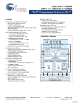
2. Logic Block Diagram
[+] Feedback

CY8C24094, CY8C24794
CY8C24894, CY8C24994
Document Number: 38-12018 Rev. *M Page 2 of 47
3. PSoC Functional Overview
The PSoC family consists of many Mixed-Signal Array with
On-Chip Controller devices. All PSoC family devices are
designed to replace traditional MCUs, system ICs, and the
numerous discrete components that surround them. The PSoC
CY8C24x94 devices are unique members of the PSoC family
because it includes a full featured, full speed (12 Mbps) USB
port. Configurable analog, digital, and interconnect circuitry
enable a high level of integration in a host of industrial,
consumer, and communication applications.
This architecture allows the user to create customized peripheral
configurations that match the requirements of each individual
application. Additionally, a fast CPU, Flash program memory,
SRAM data memory, and configurable I/O are included in a
range of convenient pinouts and packages.
The PSoC architecture, as illustrated on the left, is comprised of
four main areas: PSoC Core, Digital System, Analog System,
and System Resources including a full-speed USB port. Config-
urable global busing allows all the device resources to be
combined into a complete custom system. The PSoC
CY8C24x94 devices can have up to seven I/O ports that connect
to the global digital and analog interconnects, providing access
to 4 digital blocks and 6 analog blocks.
3.1 The PSoC Core
The PSoC Core is a powerful engine that supports a rich feature
set. The core includes a CPU, memory, clocks, and configurable
GPI/O (General Purpose I/O).
The M8C CPU core is a powerful processor with speeds up to 24
MHz, providing a four MIPS 8-bit Harvard architecture micropro-
cessor. The CPU uses an interrupt controller with up to 20
vectors, to simplify programming of real time embedded events.
Program execution is timed and protected using the included
Sleep and Watch Dog Timers (WDT).
Memory encompasses 16K of Flash for program storage, 1K of
SRAM for data storage, and up to 2K of EEPROM emulated
using the Flash. Program Flash uses four protection levels on
blocks of 64 bytes, allowing customized software IP protection.
The PSoC device incorporates flexible internal clock generators,
including a 24 MHz IMO (internal main oscillator) accurate to 8%
over temperature and voltage. The 24 MHz IMO can also be
doubled to 48 MHz for use by the digital system. A low power 32
kHz ILO (internal low speed oscillator) is provided for the Sleep
timer and WDT. The clocks, together with programmable clock
dividers (as a System Resource), provide the flexibility to
integrate almost any timing requirement into the PSoC device. In
USB systems, the IMO self tunes to ± 0.25% accuracy for USB
communication.
PSoC GPI/Os provide connection to the CPU, digital and analog
resources of the device. Each pin’s drive mode may be selected
from eight options, allowing great flexibility in external inter-
facing. Every pin is also capable of generating a system interrupt
on high level, low level, and change from last read.
3.2 The Digital System
The Digital System is composed of four digital PSoC blocks.
Each block is an 8-bit resource used alone or combined with
other blocks to form 8, 16, 24, and 32-bit peripherals, which are
called user module references.
Figure 3-1. Digital System Block Diagram
Digital peripheral configurations include those listed below.
■ Full-Speed USB (12 Mbps)
■ PWMs (8 to 32 bit)
■ PWMs with Dead band (8 to 24 bit)
■ Counters (8 to 32 bit)
■ Timers (8 to 32 bit)
■ UART 8 bit with selectable parity
■ SPI master and slave
■ I2C slave and multi-master
■ Cyclical Redundancy Checker/Generator (8 to 32 bit)
■ IrDA
■ Pseudo Random Sequence Generators (8 to 32 bit)
The digital blocks are connected to any GPI/O through a series
of global buses that can route any signal to any pin. The buses
also allow signal multiplexing and performing logic operations.
This configurability frees the designs from the constraints of a
fixed peripheral controller.
Digital blocks are provided in rows of four, where the number of
blocks varies by PSoC device family. This allows you the
optimum choice of system resources for your application. Family
resources are shown in Table 3-1 on page 4.
DIGITAL SYSTEM
To System Bus
D
i
g
i
t
a
l
C
l
o
c
k
s
F
r
o
m
C
o
r
e
Digital PSoC Block Array
To Analog
System
8
Row Input
Configuration
Row Output
Configuration
88
8
Row 0
DBB00 DBB01 DCB02 DCB03
4
4
GIE[7:0]
GIO[7:0]
GOE[7:0]
GOO[7:0]
Global Digital
Interconnect
Port 1
Port 0
Port 3
Port 2
Port 5
Port 4
Port 7
[+] Feedback

CY8C24094, CY8C24794
CY8C24894, CY8C24994
Document Number: 38-12018 Rev. *M Page 3 of 47
3.1 The Analog System
The Analog System is composed of 6 configurable blocks, each
comprised of an opamp circuit allowing the creation of complex
analog signal flows. Analog peripherals are very flexible and can
be customized to support specific application requirements.
Some of the more common PSoC analog functions (most
available as user modules) are listed below.
■ Analog-to-digital converters (up to 2, with 6 to 14-bit resolution,
selectable as Incremental, Delta Sigma, and SAR)
■ Filters (2 and 4 pole band-pass, low-pass, and notch)
■ Amplifiers (up to 2, with selectable gain to 48x)
■ Instrumentation amplifiers (1 with selectable gain to 93x)
■ Comparators (up to 2, with 16 selectable thresholds)
■ DACs (up to 2, with 6- to 9-bit resolution)
■ Multiplying DACs (up to 2, with 6- to 9-bit resolution)
■ High current output drivers (two with 30 mA drive as a PSoC
Core Resource)
■ 1.3V reference (as a System Resource)
■ DTMF Dialer
■ Modulators
■ Correlators
■ Peak Detectors
■ Many other topologies possible
Analog blocks are arranged in a column of three, which includes
one CT (Continuous Time) and two SC (Switched Capacitor)
blocks, as shown in Figure 3-2.
Figure 3-2. Analog System Block Diagram
3.0.1 The Analog Multiplexer System
The Analog Mux Bus can connect to every GPI/O pin in ports 0-5.
Pins are connected to the bus individually or in any combination.
The bus also connects to the analog system for analysis with
comparators and analog-to-digital converters. It is split into two
sections for simultaneous dual-channel processing. An
additional 8:1 analog input multiplexer provides a second path to
bring Port 0 pins to the analog array.
Switch control logic enables selected pins to precharge continu-
ously under hardware control. This enables capacitive
measurement for applications such as touch sensing. Other
multiplexer applications include:
■ Track pad, finger sensing.
■ Chip-wide mux that allows analog input from up to 48 I/O pins.
■ Crosspoint connection between any I/O pin combinations.
When designing capacitive sensing applications, refer to the
latest signal-to-noise signal level requirements Application
Notes, which are found under http://www.cypress.com > Design
Resources > Application Notes. In general, and unless otherwise
noted in the relevant Application Notes, the minimum
signal-to-noise ratio (SNR) for CapSense applications is 5:1.
ACB00 ACB01
Block
Array
Array Input
C onfig u ra tio n
ACI1[1:0]
ASD20
ACI0[1:0]
P0[6]
P0[4]
P0[2]
P0[0]
P2[2]
P2[0]
P2[6]
P2[4]
RefIn
AGNDIn
P0[7]
P0[5]
P0[3]
P0[1]
P2[3]
P2[1]
Reference
Generators
AGNDIn
R efIn
Bandgap
RefHi
RefLo
AGND
ASD11
ASC21
ASC10
Interface to
Digital System
M8C Interface (Address Bus, Data Bus, Etc.)
Analog Reference
A ll IO
(Except Port 7)
Analog
Mux Bus
[+] Feedback

CY8C24094, CY8C24794
CY8C24894, CY8C24994
Document Number: 38-12018 Rev. *M Page 4 of 47
3.1 Additional System Resources
System Resources, provide additional capability useful to
complete systems. Additional resources include a multiplier,
decimator, low voltage detection, and power on reset. Brief state-
ments describing the merits of each resource follow.
■ Full-Speed USB (12 Mbps) with 5 configurable endpoints and
256 bytes of RAM. No external components required except
two series resistors. Wider than commercial temperature USB
operation (-10°C to +85°C).
■ Digital clock dividers provide three customizable clock
frequencies for use in applications. The clocks can be routed
to both the digital and analog systems. Additional clocks are
generated using digital PSoC blocks as clock dividers.
■ Two multiply accumulates (MACs) provide fast 8-bit multipliers
with 32-bit accumulate, to assist in both general math and
digital filters.
■ Decimator provides a custom hardware filter for digital signal
processing applications including creation of Delta Sigma
ADCs.
■ The I2C module provides 100 and 400 kHz communication over
two wires. Slave, master, multi-master are supported.
■ Low Voltage Detection (LVD) interrupts signal the application
of falling voltage levels, while the advanced POR (Power On
Reset) circuit eliminates the need for a system supervisor.
■ An internal 1.3V reference provides an absolute reference for
the analog system, including ADCs and DACs.
■ Versatile analog multiplexer system.
3.2 PSoC Device Characteristics
Depending on your PSoC device characteristics, the digital and
analog systems can have 16, 8, or 4 digital blocks and 12, 6, or
4 analog blocks. The following table lists the resources available
for specific PSoC device groups. The device covered by this data
sheet is shown in the highlighted row of the table
4. Getting Started
The quickest way to understand PSoC silicon is to read this data
sheet and then use the PSoC Designer Integrated Development
Environment (IDE). This data sheet is an overview of the PSoC
integrated circuit and presents specific pin, register, and
electrical specifications.
For in depth information, along with detailed programming
details, see the PSoC® Programmable System-on-Chip
Technical Reference Manual for CY8C28xxx PSoC devices.
For up-to-date ordering, packaging, and electrical specification
information, see the latest PSoC device data sheets on the web
at www.cypress.com/psoc.
4.1 Application Notes
Application notes are an excellent introduction to the wide variety
of possible PSoC designs. They are located here:
www.cypress.com/psoc. Select Application Notes under the
Documentation tab.
4.2 Development Kits
PSoC Development Kits are available online from Cypress at
www.cypress.com/shop and through a growing number of
regional and global distributors, which include Arrow, Avnet,
Digi-Key, Farnell, Future Electronics, and Newark.
4.3 Training
Free PSoC technical training (on demand, webinars, and
workshops) is available online at www.cypress.com/training. The
training covers a wide variety of topics and skill levels to assist
you in your designs.
4.4 CyPros Consultants
Certified PSoC Consultants offer everything from technical
assistance to completed PSoC designs. To contact or become a
PSoC Consultant go to www.cypress.com/cypros.
4.5 Solutions Library
Visit our growing library of solution focused designs at
www.cypress.com/solutions. Here you can find various appli-
cation designs that include firmware and hardware design files
that enable you to complete your designs quickly.
4.6 Technical Support
For assistance with technical issues, search KnowledgeBase
articles and forums at www.cypress.com/support. If you cannot
find an answer to your question, call technical support at
1-800-541-4736.
Table 3-1. PSoC Device Characteristics
PSoC Part
Number
Digital
I/O
Digital
Rows
Digital
Blocks
Analog
Inputs
Analog
Outputs
Analog
Columns
Analog
Blocks
SRAM
Size
Flash
Size
CY8C29x66 up to
64
4 16 12 4 4 12 2K 32K
CY8C27x43 up to
44
2 8 12 4 4 12 256
Bytes
16K
CY8C24x94 56 1 4 48 2 2 6 1K 16K
CY8C24x23A up to
24
1 4 12 2 2 6 256
Bytes
4K
CY8C21x34 up to
28
1428024
[1]
512
Bytes
8K
CY8C21x23
16 1 4 8 0 2 4
[1]
256
Bytes
4K
CY8C20x34
up to
28
0 0 28 0 0 3
[2]
512
Bytes
8K
[+] Feedback

CY8C24094, CY8C24794
CY8C24894, CY8C24994
Document Number: 38-12018 Rev. *M Page 5 of 47
5. Development Tools
PSoC Designer is a Microsoft
®
Windows-based, integrated
development environment for the Programmable
System-on-Chip (PSoC) devices. The PSoC Designer IDE runs
on Windows XP or Windows Vista.
This system provides design database management by project,
an integrated debugger with In-Circuit Emulator, in-system
programming support, and built-in support for third-party
assemblers and C compilers.
PSoC Designer also supports C language compilers developed
specifically for the devices in the PSoC family.
5.1 PSoC Designer Software Subsystems
5.1.1 System-Level View
A drag-and-drop visual embedded system design environment
based on PSoC Express. In the system level view you create a
model of your system inputs, outputs, and communication inter-
faces. You define when and how an output device changes state
based upon any or all other system devices. Based upon the
design, PSoC Designer automatically selects one or more PSoC
Mixed-Signal Controllers that match your system requirements.
PSoC Designer generates all embedded code, then compiles
and links it into a programming file for a specific PSoC device.
5.1.2 Chip-Level View
The chip-level view is a more traditional integrated development
environment (IDE) based on PSoC Designer 4.4. Choose a base
device to work with and then select different onboard analog and
digital components called user modules that use the PSoC
blocks. Examples of user modules are ADCs, DACs, Amplifiers,
and Filters. Configure the user modules for your chosen
application and connect them to each other and to the proper
pins. Then generate your project. This prepopulates your project
with APIs and libraries that you can use to program your
application.
The device editor also supports easy development of multiple
configurations and dynamic reconfiguration. Dynamic
configuration allows for changing configurations at run time.
5.1.3 Hybrid Designs
You can begin in the system-level view, allow it to choose and
configure your user modules, routing, and generate code, then
switch to the chip-level view to gain complete control over
on-chip resources. All views of the project share a common code
editor, builder, and common debug, emulation, and programming
tools.
5.1.4 Code Generation Tools
PSoC Designer supports multiple third party C compilers and
assemblers. The code generation tools work seamlessly within
the PSoC Designer interface and have been tested with a full
range of debugging tools. The choice is yours.
Assemblers. The assemblers allow assembly code to merge
seamlessly with C code. Link libraries automatically use absolute
addressing or are compiled in relative mode, and linked with
other software modules to get absolute addressing.
C Language Compilers. C language compilers are available
that support the PSoC family of devices. The products allow you
to create complete C programs for the PSoC family devices.
The optimizing C compilers provide all the features of C tailored
to the PSoC architecture. They come complete with embedded
libraries providing port and bus operations, standard keypad and
display support, and extended math functionality.
5.1.5 Debugger
The PSoC Designer Debugger subsystem provides hardware
in-circuit emulation, allowing you to test the program in a physical
system while providing an internal view of the PSoC device.
Debugger commands allow the designer to read and program
and read and write data memory, read and write I/O registers,
read and write CPU registers, set and clear breakpoints, and
provide program run, halt, and step control. The debugger also
allows the designer to create a trace buffer of registers and
memory locations of interest.
5.1.6 Online Help System
The online help system displays online, context-sensitive help
for the user. Designed for procedural and quick reference, each
functional subsystem has its own context-sensitive help. This
system also provides tutorials and links to FAQs and an Online
Support Forum to aid the designer in getting started.
5.2 In-Circuit Emulator
A low cost, high functionality ICE (In-Circuit Emulator) is
available for development support. This hardware has the
capability to program single devices.
The emulator consists of a base unit that connects to the PC by
way of a USB port. The base unit is universal and operates with
all PSoC devices. Emulation pods for each device family are
available separately. The emulation pod takes the place of the
PSoC device in the target board and performs full speed (24
MHz) operation.
[+] Feedback

CY8C24094, CY8C24794
CY8C24894, CY8C24994
Document Number: 38-12018 Rev. *M Page 6 of 47
6. Designing with PSoC Designer
The development process for the PSoC device differs from that
of a traditional fixed function microprocessor. The configurable
analog and digital hardware blocks give the PSoC architecture a
unique flexibility that pays dividends in managing specification
change during development and by lowering inventory costs.
These configurable resources, called PSoC Blocks, have the
ability to implement a wide variety of user-selectable functions.
The PSoC development process can be summarized in the
following four steps:
1. Select components
2. Configure components
3. Organize and Connect
4. Generate, Verify, and Debug
6.1 Select Components
Both the system-level and chip-level views provide a library of
prebuilt, pretested hardware peripheral components. In the
system-level view, these components are called “drivers” and
correspond to inputs (a thermistor, for example), outputs (a
brushless DC fan, for example), communication interfaces
(I
2
C-bus, for example), and the logic to control how they interact
with one another (called valuators).
In the chip-level view, the components are called “user modules”.
User modules make selecting and implementing peripheral
devices simple, and come in analog, digital, and mixed signal
varieties.
6.2 Configure Components
Each of the components you select establishes the basic register
settings that implement the selected function. They also provide
parameters and properties that allow you to tailor their precise
configuration to your particular application. For example, a Pulse
Width Modulator (PWM) User Module configures one or more
digital PSoC blocks, one for each 8 bits of resolution. The user
module parameters permit you to establish the pulse width and
duty cycle. Configure the parameters and properties to
correspond to your chosen application. Enter values directly or
by selecting values from drop-down menus.
Both the system-level drivers and chip-level user modules are
documented in data sheets that are viewed directly in the PSoC
Designer. These data sheets explain the internal operation of the
component and provide performance specifications. Each data
sheet describes the use of each user module parameter or driver
property, and other information you may need to successfully
implement your design.
6.3 Organize and Connect
You can build signal chains at the chip level by interconnecting
user modules to each other and the I/O pins, or connect system
level inputs, outputs, and communication interfaces to each
other with valuator functions.
In the system-level view, selecting a potentiometer driver to
control a variable speed fan driver and setting up the valuators
to control the fan speed based on input from the pot selects,
places, routes, and configures a programmable gain amplifier
(PGA) to buffer the input from the potentiometer, an analog to
digital converter (ADC) to convert the potentiometer’s output to
a digital signal, and a PWM to control the fan.
In the chip-level view, perform the selection, configuration, and
routing so that you have complete control over the use of all
on-chip resources.
6.4 Generate, Verify, and Debug
When you are ready to test the hardware configuration or move
on to developing code for the project, perform the “Generate
Application” step. This causes PSoC Designer to generate
source code that automatically configures the device to your
specification and provides the software for the system.
Both system-level and chip-level designs generate software
based on your design. The chip-level design provides application
programming interfaces (APIs) with high level functions to
control and respond to hardware events at run-time and interrupt
service routines that you can adapt as needed. The system-level
design also generates a C main() program that completely
controls the chosen application and contains placeholders for
custom code at strategic positions allowing you to further refine
the software without disrupting the generated code.
A complete code development environment allows you to
develop and customize your applications in C, assembly
language, or both.
The last step in the development process takes place inside the
PSoC Designer’s Debugger subsystem. The Debugger
downloads the HEX image to the In-Circuit Emulator (ICE) where
it runs at full speed. Debugger capabilities rival those of systems
costing many times more. In addition to traditional single-step,
run-to-breakpoint and watch-variable features, the Debugger
provides a large trace buffer and allows you define complex
breakpoint events that include monitoring address and data bus
values, memory locations and external signals.
[+] Feedback

CY8C24094, CY8C24794
CY8C24894, CY8C24994
Document Number: 38-12018 Rev. *M Page 7 of 47
7. Document Conventions
7.1 Acronyms Used
The following table lists the acronyms that are used in this
document.
7.2 Units of Measure
A units of measure table is located in the Electrical Specifications
section. Table 10-1 on page 20 lists all the abbreviations used to
measure the PSoC devices.
7.3 Numeric Naming
Hexadecimal numbers are represented with all letters in
uppercase with an appended lowercase ‘h’ (for example, ‘14h’ or
‘3Ah’). Hexadecimal numbers may also be represented by a ‘0x’
prefix, the C coding convention. Binary numbers have an
appended lowercase ‘b’ (e.g., 01010100b’ or ‘01000011b’).
Numbers not indicated by an ‘h’ or ‘b’ are decimal.
Acronym Description
AC alternating current
ADC analog-to-digital converter
API application programming interface
CPU central processing unit
CT continuous time
DAC digital-to-analog converter
DC direct current
ECO external crystal oscillator
EEPROM electrically erasable programmable read-only
memory
FSR full scale range
GPI/O general purpose I/O
GUI graphical user interface
HBM human body model
ICE in-circuit emulator
ILO internal low speed oscillator
IMO internal main oscillator
I/O input/output
IPOR imprecise power on reset
LSb least-significant bit
LVD low voltage detect
MSb most-significant bit
PC program counter
PLL phase-locked loop
POR power on reset
PPOR precision power on reset
PSoC® Programmable System-on-Chip™
PWM pulse width modulator
SC switched capacitor
SRAM static random access memory
[+] Feedback

CY8C24094, CY8C24794
CY8C24894, CY8C24994
Document Number: 38-12018 Rev. *M Page 8 of 47
8. Pin Information
This section describes, lists, and illustrates the CY8C24x94 PSoC device family pins and pinout configuration.
The CY8C24x94 PSoC devices are available in the following packages, all of which are shown on the following pages. Every port pin
(labeled with a “P”) is capable of Digital I/O. However, Vss, Vdd, and XRES are not capable of Digital I/O.
8.1 56-Pin Part Pinout
Table 8-1. 56-Pin Part Pinout (QFN
[2]
) See LEGEND details and footnotes in Table 8-2 on page 9.
Pin
No.
Type
Name Description
Figure 8-1. CY8C24794 56-Pin PSoC Device
Digital Analog
1 I/O I, M P2[3] Direct switched capacitor block input.
2 I/O I, M P2[1] Direct switched capacitor block input.
3 I/O M P4[7]
4 I/O M P4[5]
5 I/O M P4[3]
6 I/O M P4[1]
7 I/O M P3[7]
8 I/O M P3[5]
9 I/O M P3[3]
10 I/O M P3[1]
11 I/O M P5[7]
12 I/O M P5[5]
13 I/O M P5[3]
14 I/O M P5[1]
15 I/O M P1[7] I2C Serial Clock (SCL).
16 I/O M P1[5] I2C Serial Data (SDA).
17 I/O M P1[3]
18 I/O M P1[1] I2C Serial Clock (SCL), ISSP SCLK
[1]
.
19 Power Vss Ground connection.
20 USB D+
21 USB D-
22 Power Vdd Supply voltage.
23 I/O P7[7]
24 I/O P7[0]
25 I/O M P1[0] I2C Serial Data (SDA), ISSP SDATA
[1]
.
26 I/O M P1[2]
27 I/O M P1[4] Optional External Clock Input (EXTCLK).
28 I/O M P1[6]
29 I/O M P5[0]
Pin
No.
Type
Name Description
30 I/O M P5[2]
Digital Analog
31 I/O M P5[4] 44 I/O M P2[6] External Voltage Reference (VREF) input.
32 I/O M P5[6] 45 I/O I, M P0[0] Analog column mux input.
33 I/O M P3[0] 46 I/O I, M P0[2] Analog column mux input.
34 I/O M P3[2] 47 I/O I, M P0[4] Analog column mux input VREF.
35 I/O M P3[4] 48 I/O I, M P0[6] Analog column mux input.
36 I/O M P3[6] 49 Power Vdd Supply voltage.
37 I/O M P4[0] 50 Power Vss Ground connectI/On.
38 I/O M P4[2] 51 I/O I, M P0[7] Analog column mux input,.
39 I/O M P4[4] 52 I/O I/O, M P0[5] Analog column mux input and column output.
40 I/O M P4[6] 53 I/O I/O, M P0[3] Analog column mux input and column output.
41 I/O I, M P2[0] Direct switched capacitor block input. 54 I/O I, M P0[1] Analog column mux input.
42 I/O I, M P2[2] Direct switched capacitor block input. 55 I/O M P2[7]
43 I/O M P2[4] External Analog Ground (AGND) input. 56 I/O MP2[5]
QFN
(Top View )
A, I, M, P2[3]
A, I, M, P2[1]
M, P4[7]
M, P4[5]
M, P4[3]
M, P4[1]
M, P3[7]
M, P3[5]
M, P3[3]
M, P3[1]
M, P5[7]
M, P5[5]
M, P5[3]
M, P5[1]
1
2
3
4
5
6
7
8
9
10
11
12
13
14
M, I2C SCL, P1[7]
M, I2C SDA, P1[5]
M, P1[3]
M, I2C SCL, P1[1]
Vss
D+
D-
Vdd
P7[7]
P7[0]
M, I2C SDA, P1[0]
M, P1[2]
M, P1[4]
M, P1[6]
15
16
17
18
19
20
21
22
23
24
25
26
27
28
P2[4], M
P2[6], M
P0[0], A, I, M
P0[2], A, I, M
P0[4], A, I, M
P0[6], A, I, M
Vdd
Vss
P0[7], A, I, M
P0[5], A, IO, M
P0[3], A, IO, M
P0[1], A, I, M
P2[7], M
P2[5], M
43
44
45
46
47
48
49
50
51
52
53
54
55
56
P2[2], A, I, M
P2[0], A, I, M
P4[6], M
P4[4], M
P4[2], M
P4[0], M
P3[6], M
P3[4], M
P3[2], M
P3[0], M
P5[6], M
P5[4], M
P5[2], M
P5[0], M
42
41
40
39
38
37
36
35
34
33
32
31
30
29
EXTCLK,
[+] Feedback

CY8C24094, CY8C24794
CY8C24894, CY8C24994
Document Number: 38-12018 Rev. *M Page 9 of 47
8.1 56-Pin Part Pinout (with XRES)
Table 8-2. 56-Pin Part Pinout (QFN
[2]
)
Pin
No.
Type
Name Description
Figure 8-2. CY8C24894 56-Pin PSoC Device
Digital Analog
1 I/O I, M P2[3] Direct switched capacitor block input.
2 I/O I, M P2[1] Direct switched capacitor block input.
3 I/O M P4[7]
4 I/O M P4[5]
5 I/O M P4[3]
6 I/O M P4[1]
7 I/O M P3[7]
8 I/O M P3[5]
9 I/O M P3[3]
10 I/O M P3[1]
11 I/O M P5[7]
12 I/O M P5[5]
13 I/O M P5[3]
14 I/O M P5[1]
15 I/O M P1[7] I2C Serial Clock (SCL).
16 I/O M P1[5] I2C Serial Data (SDA).
17 I/O M P1[3]
18 I/O M P1[1] I2C Serial Clock (SCL), ISSP SCLK
[1].
19 Power Vss Ground connection.
20 USB D+
21 USB D-
22 Power Vdd Supply voltage.
23 I/O P7[7]
24 I/O P7[0]
25 I/O M P1[0] I2C Serial Data (SDA), ISSP SDATA
[1]
.
26 I/O M P1[2]
27 I/O M P1[4] Optional External Clock Input (EXTCLK).
28 I/O M P1[6]
29 I/O M P5[0]
Pin
No.
Type
Name Description
30 I/O M P5[2]
Digital Analog
31 I/O M P5[4] 44 I/O M P2[6] External Voltage Reference (VREF) input.
32 I/O M P5[6] 45 I/O I, M P0[0] Analog column mux input.
33 I/O M P3[0] 46 I/O I, M P0[2] Analog column mux input.
34 I/O M P3[2] 47 I/O I, M P0[4] Analog column mux input VREF.
35 I/O M P3[4] 48 I/O I, M P0[6] Analog column mux input.
36 Input XRES Active high external reset with internal
pull down.
49 Power Vdd Supply voltage.
37 I/O M P4[0] 50 Power Vss Ground connection.
38 I/O M P4[2] 51 I/O I, M P0[7] Analog column mux input,.
39 I/O M P4[4] 52 I/O I/O, M P0[5] Analog column mux input and column output.
40 I/O M P4[6] 53 I/O I/O, M P0[3] Analog column mux input and column output.
41 I/O I, M P2[0] Direct switched capacitor block input. 54 I/O I, M P0[1] Analog column mux input.
42 I/O I, M P2[2] Direct switched capacitor block input. 55 I/O M P2[7]
43 I/O M P2[4] External Analog Ground (AGND) input. 56 I/O MP2[5]
LEGEND A = Analog, I = Input, O = Output, and M = Analog Mux Input.
QFN
(Top View)
A, I, M, P2[3]
A, I, M, P2[1]
M, P4[7 ]
M, P4[5 ]
M, P4[3 ]
M, P4[1 ]
M, P3[7 ]
M, P3[5 ]
M, P3[3 ]
M, P3[1 ]
M, P5[7 ]
M, P5[5 ]
M, P5[3 ]
M, P5[1 ]
1
2
3
4
5
6
7
8
9
10
11
12
13
14
M, I2C SCL, P1[7]
M, I2C SDA, P1[5]
M, P1[3]
M, I2C SCL, P1[1]
Vss
D+
D-
Vdd
P7[7]
P7[0]
M, I2C SDA, P1[0]
M, P1[2]
M, P1[4]
M, P1[6]
15
16
17
18
19
20
21
22
23
24
25
26
27
28
P2[4], M
P2[6], M
P0[0], A, I, M
P0[2], A, I, M
P0[4], A, I, M
P0[6], A, I, M
Vdd
Vss
P0[7], A, I, M
P0[5], A, IO, M
P0[3], A, IO, M
P0[1], A, I, M
P2[7], M
P2[5], M
43
44
45
46
47
48
49
50
51
52
53
54
55
56
P2[2], A, I, M
P2[0], A, I, M
P4[6], M
P4[4], M
P4[2], M
P4[0], M
XRES
P3[4], M
P3[2], M
P3[0], M
P5[6], M
P5[4], M
P5[2], M
P5[0], M
42
41
40
39
38
37
36
35
34
33
32
31
30
29
EXTCLK,
Notes
1. These are the ISSP pins, which are not High Z at POR. See the PSoC Programmable System-on-Chip Technical Reference Manual for details.
2. The center pad on the QFN package should be connected to ground (Vss) for best mechanical, thermal, and electrical performance. If not connected to ground, it
should be electrically floated and not connected to any other signal.
[+] Feedback

CY8C24094, CY8C24794
CY8C24894, CY8C24994
Document Number: 38-12018 Rev. *M Page 10 of 47
8.1 68-Pin Part Pinout
The 68-pin QFN part table and drawing below is for the CY8C24994 PSoC device.
Table 8-3. 68-Pin Part Pinout (QFN
[2]
)
Pin
No.
Type
Name Description
Figure 8-3. CY8C24994 68-Pin PSoC Device
Digital Analog
1 I/O M P4[7]
2 I/O M P4[5]
3 I/O MP4[3]
4 I/O MP4[1]
5 NC No connection.
6 NC No connection.
7 Power Vss Ground connection.
8 I/O M P3[7]
9 I/O M P3[5]
10 I/O MP3[3]
11 I/O MP3[1]
12 I/O M P5[7]
13 I/O M P5[5]
14 I/O MP5[3]
15 I/O MP5[1]
16 I/O M P1[7] I2C Serial Clock (SCL).
17 I/O M P1[5] I2C Serial Data (SDA).
18 I/O M P1[3]
19 I/O M P1[1] I2C Serial Clock (SCL) ISSP SCLK
[1]
.
20 Power Vss Ground connection.
21 USB D+
22 USB D-
23 Power Vdd Supply voltage.
24 I/O P7[7]
25 I/O P7[6]
26 I/O P7[5]
27 I/O P7[4]
28 I/O P7[3]
29 I/O P7[2]
Pin
No.
Type
Name Description
30 I/O P7[1] Digital Analog
31 I/O P7[0] 50 I/O M P4[6]
32 I/O M P1[0] I2C Serial Data (SDA), ISSP SDATA
[1]
.51I/O I,M P2[0] Direct switched capacitor block input.
33 I/O M P1[2] 52 I/O I,M P2[2] Direct switched capacitor block input.
34 I/O M P1[4] Optional External Clock Input (EXTCLK). 53 I/O M P2[4] External Analog Ground (AGND) input.
35 I/O M P1[6] 54 I/O M P2[6] External Voltage Reference (VREF) input.
36 I/O M P5[0] 55 I/O I,M P0[0] Analog column mux input.
37 I/O M P5[2] 56 I/O I,M P0[2] Analog column mux input and column output.
38 I/O M P5[4] 57 I/O I,M P0[4] Analog column mux input and column output.
39 I/O M P5[6] 58 I/O I,M P0[6] Analog column mux input.
40 I/O M P3[0] 59 Power Vdd Supply voltage.
41 I/O M P3[2] 60 Power Vss Ground connection.
42 I/O M P3[4] 61 I/O I,M P0[7] Analog column mux input, integration input #1
43 I/O M P3[6] 62 I/O I/O,M P0[5] Analog column mux input and column output, integration
input #2.
44
NC No connection. 63 I/O I/O,M P0[3] Analog column mux input and column output.
45
NC No connection. 64 I/O I,M P0[1] Analog column mux input.
46
Input XRES Active high pin reset with internal pull
down.
65 I/O M P2[7]
47 I/O M P4[0] 66 I/O M P2[5]
48 I/O M P4[2] 67 I/O I,M P2[3] Direct switched capacitor block input.
49
I/O M P4[4] 68 I/O I,M P2[1] Direct switched capacitor block input.
LEGENDA = Analog, I = Input, O = Output, NC = No Connection, M = Analog Mux Input.
P2[6], M, Ext. VREF
P2[4], M, Ext. AGND
M, P4[7]
M, P4[5]
M, P4[3]
M, P4[1]
NC
NC
Vss
M, P3[7]
M, P3[5]
M, P3[3]
M, P3[1]
M, P5[7]
M, P5[5]
M, P5[3]
M, P5[1]
I2C SCL, M, P1[7]
I2C SDA, M, P1[5]
M, P1[3]
P7[5]
I2C SDA, M, P1[0]
I2C SCL, M, P1[1]
Vss
D +
D -
Vdd
P7[6]
P7[4]
P7[3]
P7[2]
P7[1]
P7[0]
M, P1[2]
P2[0], M, AI
P4[6], M
P4[4], M
P4[2], M
P4[0], M
XRES
NC
NC
P3[6], M
P3[4], M
P3[2], M
P3[0], M
P5[6], M
P5[4], M
P5[2], M
P5[0], M
P1[6], M
P2[1], M, AI
P2[3], M, AI
P2[5], M
P2[7], M
P0[1], M, AI
P0[3], M, AIO
P0[5], M, AIO
P0[7], M, AI
Vss
Vdd
P0[6], M, AI
P0[4], M, AI
P0[2], M, AI
P0[0], M, AI
P2[2], M, AI
51
50
49
48
47
46
45
44
43
42
41
40
39
38
37
36
35
68
67
66
65
64
63
62
61
60
59
58
57
56
55
54
53
52
10
11
12
13
14
15
16
17
1
2
3
4
5
6
7
8
9
18
19
20
21
22
23
24
25
26
27
28
29
30
31
32
33
34
QFN
(Top View)
M, P1[4]
EXTCLK,
P7[7]
[+] Feedback

CY8C24094, CY8C24794
CY8C24894, CY8C24994
Document Number: 38-12018 Rev. *M Page 11 of 47
8.1 68-Pin Part Pinout (On-Chip Debug)
The 68-pin QFN part table and drawing below is for the CY8C24094 On-Chip Debug (OCD) PSoC device.
Note This part is only used for in-circuit debugging. It is NOT available for production.
Table 8-4. 68-Pin Part Pinout (QFN
[2]
)
Pin
No.
Type
Name Description
Figure 8-4. CY8C24094 68-Pin OCD PSoC Device
Digital Analog
1 I/O M P4[7]
2 I/O M P4[5]
3 I/O MP4[3]
4 I/O MP4[1]
5 OCDE OCD even data I/O.
6 OCDO OCD odd data output.
7 Power Vss Ground connection.
8 I/O M P3[7]
9 I/O M P3[5]
10 I/O MP3[3]
11 I/O MP3[1]
12 I/O M P5[7]
13 I/O M P5[5]
14 I/O MP5[3]
15 I/O MP5[1]
16 I/O M P1[7] I2C Serial Clock (SCL).
17 I/O M P1[5] I2C Serial Data (SDA).
18 I/O M P1[3]
19 I/O M P1[1] I2C Serial Clock (SCL), ISSP SCLK
[1]
.
20 Power Vss Ground connection.
21 USB D+
22 USB D-
23 Power Vdd Supply voltage.
24 I/O P7[7]
25 I/O P7[6]
26 I/O P7[5]
27 I/O P7[4]
28 I/O P7[3]
29 I/O P7[2]
Pin
No.
Type
Name Description
30 I/O P7[1] Digital Analog
31 I/O P7[0] 50 I/O M P4[6]
32 I/O M P1[0] I2C Serial Data (SDA), ISSP SDATA
[1]
.51I/O I,M P2[0] Direct switched capacitor block input.
33 I/O M P1[2] 52 I/O I,M P2[2] Direct switched capacitor block input.
34 I/O M P1[4] Optional External Clock Input (EXTCLK). 53 I/O M P2[4] External Analog Ground (AGND) input.
35 I/O M P1[6] 54 I/O M P2[6] External Voltage Reference (VREF) input.
36 I/O M P5[0] 55 I/O I,M P0[0] Analog column mux input.
37 I/O M P5[2] 56 I/O I,M P0[2] Analog column mux input and column output.
38 I/O M P5[4] 57 I/O I,M P0[4] Analog column mux input and column output.
39 I/O M P5[6] 58 I/O I,M P0[6] Analog column mux input.
40 I/O M P3[0] 59 Power Vdd Supply voltage.
41 I/O M P3[2] 60 Power Vss Ground connection.
42 I/O M P3[4] 61 I/O I,M P0[7] Analog column mux input, integration input #1
43 I/O M P3[6] 62 I/O I/O,M P0[5] Analog column mux input and column output,
integration input #2.
44
HCLK OCD high-speed clock output. 63 I/O I/O,M P0[3] Analog column mux input and column output.
45
CCLK OCD CPU clock output. 64 I/O I,M P0[1] Analog column mux input.
46
Input XRES Active high pin reset with internal pull
down.
65 I/O M P2[7]
47 I/O M P4[0] 66 I/O M P2[5]
48 I/O M P4[2] 67 I/O I,M P2[3] Direct switched capacitor block input.
49
I/O M P4[4] 68 I/O I,M P2[1] Direct switched capacitor block input.
LEGENDA = Analog, I = Input, O = Output, M = Analog Mux Input, OCD = On-Chip Debugger.
M, P4[7]
M, P4[5]
M, P4[3]
M, P4[1]
OCDE
OCDO
Vss
M, P3[7]
M, P3[5]
M, P3[3]
M, P3[1]
M, P5[7]
M, P5[5]
M, P5[3]
M, P5[1]
I2C SCL, M, P1[7]
I2C SDA, M, P1[5]
M, P1[3]
P7[5]
I2C SDA, M, P1[0]
I2C SCL, M, P1[1]
Vss
D +
D -
Vdd
P7[7]
P7[6]
P7[4]
P7[3]
P7[2]
P7[1]
P7[0]
M, P1[2]
M, P1[4]
P2[0], M, AI
P4[6], M
P4[4], M
P4[2], M
P4[0], M
XRES
CCLK
HCLK
P3[6], M
P3[4], M
P3[2], M
P3[0], M
P5[6], M
P5[4], M
P5[2], M
P5[0], M
P1[6], M
P2[1], M, AI
P2[3], M, AI
P2[5], M
P2[7], M
P0[1], M, AI
P0[3], M, AIO
P0[5], M, AIO
P0[7], M, AI
Vss
Vdd
P0[6], M, AI
P0[4], M, AI
P0[2], M, AI
P0[0], M, AI
P2[6], M, Ext. VREF
P2[4], M, Ext. AGND
P2[2], M, AI
51
50
49
48
47
46
45
44
43
42
41
40
39
38
37
36
35
68
67
66
65
64
63
62
61
60
59
58
57
56
55
54
53
52
10
11
12
13
14
15
16
17
1
2
3
4
5
6
7
8
9
18
19
20
21
22
23
24
25
26
27
28
29
30
31
32
33
34
QFN
(Top View)
EXTCLK
,
[+] Feedback

CY8C24094, CY8C24794
CY8C24894, CY8C24994
Document Number: 38-12018 Rev. *M Page 12 of 47
8.1 100-Ball VFBGA Part Pinout
The 100-ball VFBGA part is for the CY8C24994 PSoC device.
Table 8-5. 100-Ball Part Pinout (VFBGA)
Pin
No.
Digital
Analog
Name Description
Pin
No.
Digital
Analog
Name Description
A1 Power Vss Ground connection. F1 NC No connection.
A2 Power Vss Ground connection. F2 I/O M P5[7]
A3 NC No connection. F3 I/O M P3[5]
A4 NC No connection. F4 I/O M P5[1]
A5 NC No connection. F5 Power Vss Ground connection.
A6 Power Vdd Supply voltage. F6 Power Vss Ground connection.
A7 NC No connection. F7 I/O M P5[0]
A8 NC No connection. F8 I/O M P3[0]
A9 Power Vss Ground connection. F9 XRES Active high pin reset with internal pull down.
A10 Power Vss Ground connection. F10 I/O P7[1]
B1 Power Vss Ground connection. G1 NC No connection.
B2 Power Vss Ground connection. G2 I/O M P5[5]
B3 I/O I,M P2[1] Direct switched capacitor block input. G3 I/O M P3[3]
B4 I/O I,M P0[1] Analog column mux input. G4 I/O M P1[7] I2C Serial Clock (SCL).
B5 I/O I,M P0[7] Analog column mux input. G5 I/O M P1[1] I2C Serial Clock (SCL), ISSP SCLK
[1]
.
B6 Power Vdd Supply voltage. G6 I/O M P1[0] I2C Serial Data (SDA), ISSP SDATA
[1]
.
B7 I/O I,M P0[2] Analog column mux input. G7 I/O M P1[6]
B8 I/O I,M P2[2] Direct switched capacitor block input. G8 I/O M P3[4]
B9 Power Vss Ground connection. G9 I/O M P5[6]
B10 Power Vss Ground connection. G10 I/O P7[2]
C1 NC No connection. H1 NC No connection.
C2 I/O MP4[1] H2 I/O M P5[3]
C3 I/O MP4[7] H3 I/O M P3[1]
C4 I/O M P2[7] H4 I/O M P1[5] I2C Serial Data (SDA).
C5 I/O I/O,M P0[5] Analog column mux input and column output. H5 I/O M P1[3]
C6 I/O I,M P0[6] Analog column mux input. H6 I/O M P1[2]
C7 I/O I,M P0[0] Analog column mux input. H7 I/O M P1[4] Optional External Clock Input (EXTCLK).
C8 I/O I,M P2[0] Direct switched capacitor block input. H8 I/O M P3[2]
C9 I/O MP4[2] H9 I/O M P5[4]
C10 NC No connection. H10 I/O P7[3]
D1 NC No connection. J1 Power Vss Ground connection.
D2 I/O MP3[7] J2 Power Vss Ground connection.
D3 I/O MP4[5] J3 USB D+
D4 I/O M P2[5] J4 USB D-
D5 I/O I/O,M P0[3] Analog column mux input and column output. J5 Power Vdd Supply voltage.
D6 I/O I,M P0[4] Analog column mux input. J6 I/O P7[7]
D7 I/O M P2[6] External Voltage Reference (VREF) input. J7 I/O P7[0]
D8 I/O M P4[6] J8 I/O M P5[2]
D9 I/O M P4[0] J9 Power Vss Ground connection.
D10 NC No connection. J10 Power Vss Ground connection.
E1 NC No connection. K1 Power Vss Ground connection.
E2 NC No connection. K2 Power Vss Ground connection.
E3 I/O MP4[3] K3 NC No connection.
E4 I/O I,M P2[3] Direct switched capacitor block input. K4 NC No connection.
E5 Power Vss Ground connection. K5 Power Vdd Supply voltage.
E6 Power Vss Ground connection. K6 I/O P7[6]
E7 I/O M P2[4] External Analog Ground (AGND) input. K7 I/O P7[5]
E8 I/O M P4[4] K8 I/O P7[4]
E9 I/O M P3[6] K9 Power Vss Ground connection.
E10 NC No connection. K10 Power Vss Ground connection.
LEGENDA = Analog, I = Input, O = Output, M = Analog Mux Input, NC = No Connection.
[+] Feedback

CY8C24094, CY8C24794
CY8C24894, CY8C24994
Document Number: 38-12018 Rev. *M Page 13 of 47
Figure 8-5. CY8C24094 OCD (Not for Production)
8.1 100-Ball VFBGA Part Pinout (On-Chip Debug)
The 100-pin VFBGA part table and drawing below is for the CY8C24094 On-Chip Debug (OCD) PSoC device.
Note This part is only used for in-circuit debugging. It is NOT available for production.
Table 8-6. 100-Ball Part Pinout (VFBGA)
Pin
No.
Digital
Analog
Name Description
Pin
No.
Digital
Analog
Name Description
A1 Power Vss Ground connection. F1 OCDE OCD even data I/O.
A2 Power Vss Ground connection. F2 I/O M P5[7]
A3 NC No connection. F3 I/O M P3[5]
A4 NC No connection. F4 I/O M P5[1]
A5 NC No connection. F5 Power Vss Ground connection.
A6 Power Vdd Supply voltage. F6 Power Vss Ground connection.
A7 NC No connection. F7 I/O M P5[0]
A8 NC No connection. F8 I/O M P3[0]
A9 Power Vss Ground connection. F9 XRES Active high pin reset with internal pull down.
A10 Power Vss Ground connection. F10 I/O P7[1]
B1 Power Vss Ground connection. G1 OCDO OCD odd data output.
B2 Power Vss Ground connection. G2 I/O M P5[5]
B3 I/O I,M P2[1] Direct switched capacitor block input. G3 I/O M P3[3]
B4 I/O I,M P0[1] Analog column mux input. G4 I/O M P1[7] I2C Serial Clock (SCL).
B5 I/O I,M P0[7] Analog column mux input. G5 I/O M P1[1] I2C Serial Clock (SCL), ISSP SCLK
[1]
.
B6 Power Vdd Supply voltage. G6 I/O M P1[0] I2C Serial Data (SDA), ISSP SDATA
[1]
.
B7 I/O I,M P0[2] Analog column mux input. G7 I/O M P1[6]
B8 I/O I,M P2[2] Direct switched capacitor block input. G8 I/O M P3[4]
B9 Power Vss Ground connection. G9 I/O M P5[6]
B10 Power Vss Ground connection. G10 I/O P7[2]
C1 NC No connection. H1 NC No connection.
C2 I/O MP4[1] H2 I/O M P5[3]
C3 I/O MP4[7] H3 I/O M P3[1]
C4 I/O M P2[7] H4 I/O M P1[5] I2C Serial Data (SDA).
C5 I/O I/O,
M
P0[5] Analog column mux input and column output. H5 I/O M P1[3]
C6 I/O I,M P0[6] Analog column mux input. H6 I/O M P1[2]
C7 I/O I,M P0[0] Analog column mux input. H7 I/O M P1[4] Optional External Clock Input (EXTCLK).
Vss Vss NC NC NC Vdd NC NC Vss Vss
Vss Vss P2[1] P0[1] P0[7] Vdd P0[2] P2[2] Vss Vss
NC P4[1] P4[7] P2[7] P0[5] P0[6] P0[0] P2[0] P4[2] NC
NC P3[7] P4[5] P2[5] P0[3] P0[4] P2[6] P4[6] P4[0] NC
NC NC P4[3] P2[3] Vss Vss P2[4] P4[4] P3[6] NC
NC P5[7] P3[5] P5[1] Vss Vss P5[0] P3[0] XRES P7[1]
NC P5[5] P3[3] P1[7] P1[1] P1[0] P1[6] P3[4] P5[6] P7[2]
NC P5[3] P3[1] P1[5] P1[3] P1[2] P1[4] P3[2] P5[4] P7[3]
Vss Vss D + D - Vdd P7[7] P7[0] P5[2] Vss Vss
Vss Vss NC NC Vdd P7[6] P7[5] P7[4] Vss Vss
12345678910
A
B
C
D
E
F
G
H
J
K
BGA (Top View)
[+] Feedback

CY8C24094, CY8C24794
CY8C24894, CY8C24994
Document Number: 38-12018 Rev. *M Page 14 of 47
Figure 8-6. CY8C24094 OCD (Not for Production)
C8 I/O I,M P2[0] Direct switched capacitor block input. H8 I/O M P3[2]
C9 I/O MP4[2] H9 I/O M P5[4]
C10 NC No connection. H10 I/O P7[3]
D1 NC No connection. J1 Power Vss Ground connection.
D2 I/O MP3[7] J2 Power Vss Ground connection.
D3 I/O MP4[5] J3 USB D+
D4 I/O M P2[5] J4 USB D-
D5 I/O I/O,
M
P0[3] Analog column mux input and column output. J5 Power Vdd Supply voltage.
D6 I/O I,M P0[4] Analog column mux input. J6 I/O P7[7]
D7 I/O M P2[6] External Voltage Reference (VREF) input. J7 I/O P7[0]
D8 I/O M P4[6] J8 I/O M P5[2]
D9 I/O M P4[0] J9 Power Vss Ground connection.
D10 CCLK OCD CPU clock output. J10 Power Vss Ground connection.
E1 NC No connection. K1 Power Vss Ground connection.
E2 NC No connection. K2 Power Vss Ground connection.
E3 I/O MP4[3] K3 NC No connection.
E4 I/O I,M P2[3] Direct switched capacitor block input. K4 NC No connection.
E5 Power Vss Ground connection. K5 Power Vdd Supply voltage.
E6 Power Vss Ground connection. K6 I/O P7[6]
E7 I/O M P2[4] External Analog Ground (AGND) input. K7 I/O P7[5]
E8 I/O M P4[4] K8 I/O P7[4]
E9 I/O M P3[6] K9 Power Vss Ground connection.
E10 HCLK OCD high-speed clock output. K10 Power Vss Ground connection.
LEGENDA = Analog, I = Input, O = Output, M = Analog Mux Input, NC = No Connection, OCD = On-Chip Debugger.
Table 8-6. 100-Ball Part Pinout (VFBGA) (continued)
Vss Vss NC NC NC Vdd NC NC Vss Vss
Vss Vss P2[1] P0[1] P0[7] Vdd P0[2] P2[2] Vss Vss
NC P4[1] P4[7] P2[7] P0[5] P0[6] P0[0] P2[0] P4[2] NC
NC P3[7] P4[5] P2[5] P0[3] P0[4] P2[6] P4[6] P4[0] CClk
NC NC P4[3] P2[3] Vss Vss P2[4] P4[4] P3[6] HClk
ocde P5[7] P3[5] P5[1] Vss Vss P5[0] P3[0] XRES P7[1]
ocdo P5[5] P3[3] P1[7] P1[1] P1[0] P1[6] P3[4] P5[6] P7[2]
NC P5[3] P3[1] P1[5] P1[3] P1[2] P1[4] P3[2] P5[4] P7[3]
Vss Vss D + D - Vdd P7[7] P7[0] P5[2] Vss Vss
Vss Vss NC NC Vdd P7[6] P7[5] P7[4] Vss Vss
12345678910
A
B
C
D
E
F
G
H
J
K
BGA (Top View)
[+] Feedback

CY8C24094, CY8C24794
CY8C24894, CY8C24994
Document Number: 38-12018 Rev. *M Page 15 of 47
8.1 100-Pin Part Pinout (On-Chip Debug)
The 100-pin TQFP part is for the CY8C24094 On-Chip Debug (OCD) PSoC device.
Note This part is only used for in-circuit debugging. It is NOT available for production.
Table 8-7. 100-Pin Part Pinout (TQFP)
Pin
No.
Digital
Analog
Name Description
Pin
No.
Digital
Analog
Name Description
1 NC No connection. 51 I/O M P1[6]
2 NC No connection. 52 I/O M P5[0]
3 I/O I, M P0[1] Analog column mux input. 53 I/O M P5[2]
4 I/O M P2[7] 54 I/O M P5[4]
5 I/O M P2[5] 55 I/O M P5[6]
6 I/O I, M P2[3] Direct switched capacitor block input. 56 I/O M P3[0]
7 I/O I, M P2[1] Direct switched capacitor block input. 57 I/O M P3[2]
8 I/O M P4[7] 58 I/O M P3[4]
9 I/O M P4[5] 59 I/O M P3[6]
10 I/O M P4[3] 60 HCLK OCD high-speed clock output.
11 I/O M P4[1] 61 CCLK OCD CPU clock output.
12 OCDE OCD even data I/O. 62 Input XRES Active high pin reset with internal pull down.
13 OCDO OCD odd data output. 63 I/O M P4[0]
14 NC No connection. 64 I/O M P4[2]
15 Power Vss Ground connection. 65 Power Vss Ground connection.
16 I/O M P3[7] 66 I/O M P4[4]
17 I/O M P3[5] 67 I/O M P4[6]
18 I/O M P3[3] 68 I/O I, M P2[0] Direct switched capacitor block input.
19 I/O M P3[1] 69 I/O I, M P2[2] Direct switched capacitor block input.
20 I/O M P5[7] 70 I/O P2[4] External Analog Ground (AGND) input.
21 I/O M P5[5] 71 NC No connection.
22 I/O M P5[3] 72 I/O P2[6] External Voltage Reference (VREF) input.
23 I/O M P5[1] 73 NC No connection.
24 I/O M P1[7] I2C Serial Clock (SCL). 74 I/O I P0[0] Analog column mux input.
25 NC No connection. 75 NC No connection.
26 NC No connection. 76 NC No connection.
27 NC No connection. 77 I/O I, M P0[2] Analog column mux input and column output.
28 I/O P1[5] I2C Serial Data (SDA) 78 NC No connection.
29 I/O P1[3] 79 I/O I, M P0[4] Analog column mux input and column output.
30 I/O P1[1] Crystal (XTALin), I2C Serial Clock (SCL),
ISSP SCLK
[1]
.
80
NC No connection.
31 NC No connection. 81 I/O I, M P0[6] Analog column mux input.
32 Power Vss Ground connection. 82 Power Vdd Supply voltage.
33 USB D+ 83 NC No connection.
34 USB D- 84 Power Vss Ground connection.
35 Power Vdd Supply voltage. 85 NC No connection.
36 I/O P7[7] 86 NC No connection.
37 I/O P7[6] 87 NC No connection.
38 I/O P7[5] 88 NC No connection.
39 I/O P7[4] 89 NC No connection.
40 I/O P7[3] 90 NC No connection.
41 I/O P7[2] 91 NC No connection.
42 I/O P7[1] 92 NC No connection.
43 I/O P7[0] 93 NC No connection.
44 NC No connection. 94 NC No connection.
45 NC No connection. 95 I/O I, M P0[7] Analog column mux input.
46 NC No connection. 96 NC No connection.
47 NC No connection. 97 I/O I/O,
M
P0[5] Analog column mux input and column output.
48 I/O P1[0] Crystal (XTALout), I2C Serial Data (SDA),
ISSP SDATA
[1]
.
98 NC No connection.
49 I/O P1[2] 99 I/O I/O,
M
P0[3] Analog column mux input and column output.
50 I/O P1[4] Optional External Clock Input (EXTCLK). 100 NC No connection.
[+] Feedback

CY8C24094, CY8C24794
CY8C24894, CY8C24994
Document Number: 38-12018 Rev. *M Page 16 of 47
Figure 8-7. CY8C24094 OCD (Not for Production)
LEGENDA = Analog, I = Input, O = Output, NC = No Connection, M = Analog Mux Input, OCD = On-Chip Debugger.
Table 8-7. 100-Pin Part Pinout (TQFP) (continued)
TQFP
NC
NC
AI, M, P0[1]
M, P2[7]
M, P2[5]
AI, M, P2[3]
AI, M, P2[1]
M, P4[7]
M, P4[5]
M, P4[3]
M, P4[1]
OCDE
OCDO
NC
Vss
M, P3[7]
M, P3[5]
M, P3[3]
M, P3[1]
M, P5[7]
M, P5[5]
M, P5[3]
M, P5[1]
I2C SCL, P1[7]
NC
NC
D-
P7[3]
NC
NC
I2C SDA, M, P1[5]
M, P1[3]
I2C SCL, M, P1[1]
NC
Vss
D+
Vdd
P7[7]
P7[6]
P7[5]
P7[4]
P7[2]
P7[1]
P7[0]
NC
NC
NC
I2C SDA, M, P1[0]
M, P1[2]
M, P1[4]
NC
P0[0], M, AI
NC
P2[6], M, External VREF
NC
P2[4], M, External AGND
P2[2], M, AI
P2[0], M, AI
P4[6], M
P4[4], M
Vss
P4[2], M
P4[0], M
XRES
CCLK
HCLK
P3[6], M
P3[4], M
P3[2], M
P3[0], M
P5[6], M
P5[4], M
P5[2], M
P5[0], M
P1[6], M
NC
P0[3], M, AI
NC
P0[5], M, AI
NC
P0[7], M, AI
NC
NC
NC
NC
NC
NC
NC
NC
NC
NC
Vss
NC
Vdd
P0[6], M, AI
NC
P0[4], M, AI
NC
P0[2], M, AI
NC
75
74
73
72
71
70
69
68
67
66
65
64
63
62
61
60
59
58
57
56
55
54
53
52
51
100
99
98
97
96
95
94
93
92
91
90
89
88
87
86
85
84
83
82
81
80
79
78
77
76
10
11
12
13
14
15
16
17
18
19
20
21
22
23
24
25
1
2
3
4
5
6
7
8
9
26
27
28
29
30
31
32
33
34
35
36
37
38
39
40
41
42
43
44
45
46
47
48
50
49
EXTCLK,
[+] Feedback

CY8C24094, CY8C24794
CY8C24894, CY8C24994
Document Number: 38-12018 Rev. *M Page 17 of 47
9. Register Reference
This section lists the registers of the CY8C24x94 PSoC device family. For detailed register information, reference the
PSoC Programmable System-on-Chip Technical Reference Manual.
9.1 Register Conventions
The register conventions specific to this section are listed in the
following table.
9.2 Register Mapping Tables
The PSoC device has a total register address space of 512
bytes. The register space is referred to as I/O space and is
divided into two banks. The XOI bit in the Flag register (CPU_F)
determines which bank the user is currently in. When the XOI bit
is set the user is in Bank 1.
Note In the following register mapping tables, blank fields are
Reserved and should not be accessed.
Convention Description
R Read register or bit(s)
W Write register or bit(s)
L Logical register or bit(s)
C Clearable register or bit(s)
# Access is bit specific
[+] Feedback

CY8C24094, CY8C24794
CY8C24894, CY8C24994
Document Number: 38-12018 Rev. *M Page 18 of 47
9.3 Register Map Bank 0 Table: User Space
Name Addr (0,Hex) Access Name Addr (0,Hex) Access Name Addr (0,Hex) Access Name Addr (0,Hex) Access
PRT0DR 00 RW PMA0_DR 40 RW ASC10CR0 80 RW C0
PRT0IE 01 RW PMA1_DR 41 RW ASC10CR1 81 RW C1
PRT0GS 02 RW PMA2_DR 42 RW ASC10CR2 82 RW C2
PRT0DM2 03 RW PMA3_DR 43 RW ASC10CR3 83 RW C3
PRT1DR 04 RW PMA4_DR 44 RW ASD11CR0 84 RW C4
PRT1IE 05 RW PMA5_DR 45 RW ASD11CR1 85 RW C5
PRT1GS 06 RW PMA6_DR 46 RW ASD11CR2 86 RW C6
PRT1DM2 07 RW PMA7_DR 47 RW ASD11CR3 87 RW C7
PRT2DR 08 RW USB_SOF0 48 R 88 C8
PRT2IE 09 RW USB_SOF1 49 R 89 C9
PRT2GS 0A RW USB_CR0 4A RW 8A CA
PRT2DM2 0B RW USBI/O_CR0 4B # 8B CB
PRT3DR 0C RW USBI/O_CR1 4C RW 8C CC
PRT3IE 0D RW 4D 8D CD
PRT3GS 0E RW EP1_CNT1 4E # 8E CE
PRT3DM2 0F RW EP1_CNT 4F RW 8F CF
PRT4DR 10 RW EP2_CNT1 50 # ASD20CR0 90 RW CUR_PP D0 RW
PRT4IE 11 RW EP2_CNT 51 RW ASD20CR1 91 RW STK_PP D1 RW
PRT4GS 12 RW EP3_CNT1 52 # ASD20CR2 92 RW D2
PRT4DM2 13 RW EP3_CNT 53 RW ASD20CR3 93 RW IDX_PP D3 RW
PRT5DR 14 RW EP4_CNT1 54 # ASC21CR0 94 RW MVR_PP D4 RW
PRT5IE 15 RW EP4_CNT 55 RW ASC21CR1 95 RW MVW_PP D5 RW
PRT5GS 16 RW EP0_CR 56 # ASC21CR2 96 RW I2C_CFG D6 RW
PRT5DM2 17 RW EP0_CNT 57 # ASC21CR3 97 RW I2C_SCR D7 #
18 EP0_DR0 58 RW 98 I2C_DR D8 RW
19 EP0_DR1 59 RW 99 I2C_MSCR D9 #
1A EP0_DR2 5A RW 9A INT_CLR0 DA RW
1B EP0_DR3 5B RW 9B INT_CLR1 DB RW
PRT7DR 1C RW EP0_DR4 5C RW 9C INT_CLR2 DC RW
PRT7IE 1D RW EP0_DR5 5D RW 9D INT_CLR3 DD RW
PRT7GS 1E RW EP0_DR6 5E RW 9E INT_MSK3 DE RW
PRT7DM2 1F RW EP0_DR7 5F RW 9F INT_MSK2 DF RW
DBB00DR0 20 # AMX_IN 60 RW A0 INT_MSK0 E0 RW
DBB00DR1 21 W AMUXCFG 61 RW A1 INT_MSK1 E1 RW
DBB00DR2 22 RW 62 A2 INT_VC E2 RC
DBB00CR0 23 # ARF_CR 63 RW A3 RES_WDT E3 W
DBB01DR0 24 # CMP_CR0 64 # A4 DEC_DH E4 RC
DBB01DR1 25 W ASY_CR 65 # A5 DEC_DL E5 RC
DBB01DR2 26 RW CMP_CR1 66 RW A6 DEC_CR0 E6 RW
DBB01CR0 27 # 67 A7 DEC_CR1 E7 RW
DCB02DR0 28 # 68 MUL1_X A8 W MUL0_X E8 W
DCB02DR1 29 W 69 MUL1_Y A9 W MUL0_Y E9 W
DCB02DR2 2A RW 6A MUL1_DH AA R MUL0_DH EA R
DCB02CR0 2B # 6B MUL1_DL AB R MUL0_DL EB R
DCB03DR0 2C # TMP_DR0 6C RW ACC1_DR1 AC RW ACC0_DR1 EC RW
DCB03DR1 2D W TMP_DR1 6D RW ACC1_DR0 AD RW ACC0_DR0 ED RW
DCB03DR2 2E RW TMP_DR2 6E RW ACC1_DR3 AE RW ACC0_DR3 EE RW
DCB03CR0 2F # TMP_DR3 6F RW ACC1_DR2 AF RW ACC0_DR2 EF RW
30
ACB00CR3 70 RW RDI0RI B0 RW F0
31
ACB00CR0 71 RW RDI0SYN B1 RW F1
32
ACB00CR1 72 RW RDI0IS B2 RW F2
33
ACB00CR2 73 RW RDI0LT0 B3 RW F3
34
ACB01CR3 74 RW RDI0LT1 B4 RW F4
35
ACB01CR0 75 RW RDI0RO0 B5 RW F5
36
ACB01CR1 76 RW RDI0RO1 B6 RW F6
37
ACB01CR2 77 RW B7 CPU_F F7 RL
38
78 B8 F8
39
79 B9 F9
3A
7A BA FA
3B
7B BB FB
3C
7C BC FC
3D
7D BD DAC_D FD RW
3E
7E BE CPU_SCR1 FE #
3F
7F BF CPU_SCR0 FF #
Blank fields are Reserved and should not be accessed. # Access is bit specific.
[+] Feedback

CY8C24094, CY8C24794
CY8C24894, CY8C24994
Document Number: 38-12018 Rev. *M Page 19 of 47
9.4 Register Map Bank 1 Table: Configuration Space
Name Addr (1,Hex) Access Name Addr (1,Hex) Access Name Addr (1,Hex) Access Name Addr (1,Hex) Access
PRT0DM0 00 RW PMA0_WA 40 RW ASC10CR0 80 RW USBI/O_CR2 C0 RW
PRT0DM1 01 RW PMA1_WA 41 RW ASC10CR1 81 RW USB_CR1 C1 #
PRT0IC0 02 RW PMA2_WA 42 RW ASC10CR2 82 RW
PRT0IC1 03 RW PMA3_WA 43 RW ASC10CR3 83 RW
PRT1DM0 04 RW PMA4_WA 44 RW ASD11CR0 84 RW EP1_CR0 C4 #
PRT1DM1 05 RW PMA5_WA 45 RW ASD11CR1 85 RW EP2_CR0 C5 #
PRT1IC0 06 RW PMA6_WA 46 RW ASD11CR2 86 RW EP3_CR0 C6 #
PRT1IC1 07 RW PMA7_WA 47 RW ASD11CR3 87 RW EP4_CR0 C7 #
PRT2DM0 08 RW 48 88 C8
PRT2DM1 09 RW 49 89 C9
PRT2IC0 0A RW 4A 8A CA
PRT2IC1 0B RW 4B 8B CB
PRT3DM0 0C RW 4C 8C CC
PRT3DM1 0D RW 4D 8D CD
PRT3IC0 0E RW 4E 8E CE
PRT3IC1 0F RW 4F 8F CF
PRT4DM0 10 RW PMA0_RA 50 RW 90 GDI_O_IN D0 RW
PRT4DM1 11 RW PMA1_RA 51 RW ASD20CR1 91 RW GDI_E_IN D1 RW
PRT4IC0 12 RW PMA2_RA 52 RW ASD20CR2 92 RW GDI_O_OU D2 RW
PRT4IC1 13 RW PMA3_RA 53 RW ASD20CR3 93 RW GDI_E_OU D3 RW
PRT5DM0 14 RW PMA4_RA 54 RW ASC21CR0 94 RW D4
PRT5DM1 15 RW PMA5_RA 55 RW ASC21CR1 95 RW D5
PRT5IC0 16 RW PMA6_RA 56 RW ASC21CR2 96 RW D6
PRT5IC1 17 RW PMA7_RA 57 RW ASC21CR3 97 RW D7
18 58 98 MUX_CR0 D8 RW
19 59 99 MUX_CR1 D9 RW
1A 5A 9A MUX_CR2 DA RW
1B 5B 9B MUX_CR3 DB RW
PRT7DM0 1C RW 5C 9C DC
PRT7DM1 1D RW 5D 9D OSC_GO_EN DD RW
PRT7IC0 1E RW 5E 9E OSC_CR4 DE RW
PRT7IC1 1F RW 5F 9F OSC_CR3 DF RW
DBB00FN 20 RW CLK_CR0 60 RW A0 OSC_CR0 E0 RW
DBB00IN 21 RW CLK_CR1 61 RW A1 OSC_CR1 E1 RW
DBB00OU 22 RW ABF_CR0 62 RW A2 OSC_CR2 E2 RW
23 AMD_CR0 63 RW A3 VLT_CR E3 RW
DBB01FN 24 RW CMP_GO_EN 64 RW A4 VLT_CMP E4 R
DBB01IN 25 RW 65 A5 E5
DBB01OU 26 RW AMD_CR1 66 RW A6 E6
27 ALT_CR0 67 RW A7 E7
DCB02FN 28 RW 68 A8 IMO_TR E8 W
DCB02IN 29 RW 69 A9 ILO_TR E9 W
DCB02OU 2A RW 6A AA BDG_TR EA RW
2B 6B AB ECO_TR EB W
DCB03FN 2C RW TMP_DR0 6C RW AC MUX_CR4 EC RW
DCB03IN 2D RW TMP_DR1 6D RW AD MUX_CR5 ED RW
DCB03OU 2E RW TMP_DR2 6E RW AE EE
2F TMP_DR3 6F RW AF EF
30
ACB00CR3 70 RW RDI0RI B0 RW F0
31
ACB00CR0 71 RW RDI0SYN B1 RW F1
32
ACB00CR1 72 RW RDI0IS B2 RW F2
33 ACB00CR2 73 RW RDI0LT0 B3 RW F3
34
ACB01CR3 74 RW RDI0LT1 B4 RW F4
35
ACB01CR0 75 RW RDI0RO0 B5 RW F5
36
ACB01CR1 76 RW RDI0RO1 B6 RW F6
37 ACB01CR2 77 RW B7 CPU_F F7 RL
38
78 B8 F8
39
79 B9 F9
3A
7A BA FA
3B 7B BB FB
3C
7C BC FC
3D
7D BD DAC_CR FD RW
3E
7E BE CPU_SCR1 FE #
3F 7F BF CPU_SCR0 FF #
Blank fields are Reserved and should not be accessed. # Access is bit specific.
[+] Feedback

CY8C24094, CY8C24794
CY8C24894, CY8C24994
Document Number: 38-12018 Rev. *M Page 20 of 47
10. Electrical Specifications
This section presents the DC and AC electrical specifications of the CY8C24x94 PSoC device family. For the most up to date electrical
specifications, confirm that you have the most recent data sheet by going to the web at http://www.cypress.com/psoc.
Specifications are valid for -40
o
C ≤ T
A
≤ 85
o
C and T
J
≤ 100
o
C, except where noted. Specifications for devices running at greater than
12 MHz are valid for -40
o
C ≤ T
A
≤ 70
o
C and T
J
≤ 82
o
C.
Figure 10-1. Voltage versus CPU Frequency
The following table lists the units of measure that are used in this chapter.
Table 10-1. Units of Measure
Symbol Unit of Measure Symbol Unit of Measure
o
C degree Celsius μW microwatts
dB decibels mA milli-ampere
fF femto farad ms milli-second
Hz hertz mV milli-volts
KB 1024 bytes nA nanoampere
Kbit 1024 bits ns nanosecond
kHz kilohertz nV nanovolts
kΩ kilohm W ohm
MHz megahertz pA picoampere
MΩ megaohm pF picofarad
μA microampere pp peak-to-peak
μF microfarad ppm parts per million
μH microhenry ps picosecond
μs microsecond sps samples per second
μV microvolts s sigma: one standard deviation
μVrms microvolts root-mean-square V volts
5.25
4.75
3.00
93 kHz 12 MHz 24 MHz
CPU Frequency
Vdd Voltage
V
a
l
i
d
O
p
e
r
a
t
i
n
g
R
e
g
i
o
n
[+] Feedback
/