Page is loading ...

Schematic Review Checklist for
West Bridge
®
Astoria™
December 12, 2008 Document No. 001-46860 Rev. *A 1
AN46860
Author: Praveen Kumar
Associated Project: No
Software Version: Astoria SDK 1.0
Associated Application Notes: None
Application Note Abstract
West Bridge
®
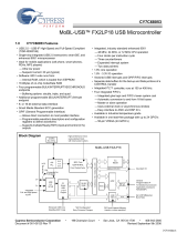
Astoria™ is a USB and mass storage peripheral control device that contains three main ports: processor
interface (P-port), mass storage support (S-port), and USB interface (U-port). This application note discusses the hardware
recommendations and guidelines to design a system using Astoria.
Introduction
The West Bridge
®
Astoria™ device is a peripheral controller
that supports high speed USB and mass storage access.
This controller provides access from a processor interface
and a high speed USB (HS-USB) interface to peripherals
including SD, MMC/MMC+, CE-ATA, SDIO, SLC, and MLC
NAND. It supports interleaving accesses between the
processor interface, HS-USB, and peripherals. This enables
an external processor and an external USB host to transfer
data simultaneously to each other and to the mass storage
peripherals.
The hardware considerations to design Astoria into a system
are:
P-Port
1. If operating in the asynchronous mode, CLK is tied
LOW through a 10k resistor. In the synchronous mode,
CLK is connected to the incoming signal from the
processor interface.
2. In PCRAM and ADM mode, ADV# is tied to a signal on
the processor interface that conforms to the timing
specified in the West Bridge: Antioch USB/Mass
Storage Peripheral Controller data sheet. If the signal is
not available, tie ADV# to the CE# signal of the
processor interface.
3. The DRQ Status Register and DRQ Mask Register
indicate the available endpoints for transfer. They must
be accessed even if a DMA or burst operation is not
being implemented on the P-port interface. Use the
DRQ# or the INT# signal to indicate to the processor
that at least one of the bits in the DRQ Status Register
is set. If INT# is used, an extra read of the P-port
Interrupt Register must be done before the DRQ Status
Register is read. In PNAND mode, R/B is used as an
indication of End Point availability and is treated
differently in LNA and nonLNA modes.
4. Ensure that TEST[2:0], A7, A3, and A2 settings are
correct for the various P-port interface configurations.
Table 1 lists the TEST[2:0] and register settings for
P-port interface configurations.
Table 1. P-Port Interface Configuration Options
TEST
[2:0]
VMTYPE Field in
CY_AN_MEM_P0_VM_S
ET Register
Interface
000
101
Non ADM PCRAM
000
111
SRAM
010
X
Extended Interface Mode
Table 2 lists the TEST[2:0] and address pin settings for
the various extended interface modes.
Table 2. Extended Interface Modes
TEST
[2:0]
A7
A3
A2
Interface
010
1
0
0
PNAND Mode-Small Block Device
010
0
0
0
PNAND Mode-Large Block Device
010
1
0
1
Address/Data Bus Multiplexing
(ADM)
010
1
1
0
SPI Mode
5. When using extended P-port modes, SCL and SDA (A5
and A6) require external pull up. The pull up resistors
are determined by the supply voltage, clock speed, and
bus capacitance. A typical value for the I2C pull ups is
2 kΩ. This value must be adjusted based on the trace
length and board layout conditions. The pull up on SDA
is required even if I
2
C™ EEPROM is not being used. A
low value resistor can cause overshoot and a high
value resistor can cause timing violation depending on
the capacitance on the bus.
[+] Feedback

AN46860
December 12, 2008 Document No. 001-46860 Rev. *A 2
6. DACK# is used in conjunction with DRQ#. If INT# is
used to indicate that at least one bit is set in the DRQ#
register, then DACK# remains unused. DACK# is not
required for Astoria to function.
7. INT#, DRQ#, and DACK# are in GVVDQ power
domain. Therefore, pull up the input pin DACK# to
GVDDQ using a 10k resistor, if it is not used.
8. All unused inputs and input or output pins on the P-port
are tied to a valid logic level (HIGH for lowest leakage)
through a 10k resistor. Use a single resistor for all
unused pins. When pulling HIGH, the unused pins are
tied to the appropriate power domain, in this case,
PVDDQ or GVDDQ.
Refer to the Pin Assignments table in the data sheet for
more details on pin configuration for each P-port
interface mode and their corresponding power domains.
9. The INT# and DRQ# signals float when Astoria is in
Standby state. These signals are active low. As a result,
a pull up resistor must be connected to these signals to
prevent the P-port processor from receiving any false
interrupts.
10. In the PNAND Interface Mode, external pull up is not
required for the R/B# signal. R/B# signal is not an open
drain or collector output.
S-Port
1. Use SD_D[3]/SD2_D[3] or GPIO[0]/GPIO[1] to detect
cards on Astoria. If SD_D[3]/SD2_D[3] is used, then it
must be pulled down using a 470 kΩ resistor.
2. Treat the SD_CLK signal as a high speed signal
switching at a maximum of 48 MHz to determine the
appropriate signal integrity precautions.
3. If you are designing an application supporting SD/MMC
and CE-ATA, follow the trace length restrictions.
Table 3 lists acceptable frequencies for Astoria, and the
maximum trace lengths corresponding to the
frequencies for SD cards that cannot operate in high
speed mode.
Table 3. Frequency vs. Trace Length (SD Default Mode)
SDFREQ (MHz)
Maximum Trace Length (in)
24.00
1.94
21.82
7.55
20.00
13.17
18.46
18.78
17.14
24.4
Table 4 lists the acceptable frequencies for Astoria and
the corresponding maximum trace lengths for SD cards
that are capable of operating in high speed mode.
Table 4. Frequency vs. Trace Length (SD High Speed
Mode)
SDFREQ (MHz)
Maximum Trace Length (in)
48.00
8.18
40.00
20.66
34.29
33.13
30.00
45.61
26.67
58.08
Refer to the Pin Assignments table in the data sheet for
more details on pin configuration for each pin in each
S-port configuration and their corresponding power
domains.
4. All unused inputs and input or output pins on the S-port
are tied to a valid logic level (HIGH for lowest leakage)
through a 10k resistor. Use a single resistor for all
unused pins. When pulling HIGH, the unused pins are
tied to the appropriate power domain, in this case,
SSVDDQ, SNVDDQ, or GVDDQ.
5. The pull up resistor (Rp) used for NAND_R/B# varies
from 1k to 10k based on the timing requirements and
the manufacturer of the NAND device.
6. The SD_POW signal floats when Astoria is in standby.
If this signal is used to control power to the SD card
through an external switch, a pull up or pull down
resistor must be connected on SD_POW, such that the
switch remains ON and power to the card is retained
during Astoria’s standby condition.
U-Port
1. To avoid an impedance mismatch, lay out the USB
differential signals (D+ and D-) with constant spacing
and on one plane. Avoid vias and stubs. It is prudent to
lay out the signals before laying out the rest of the
board.
2. Minimize the trace lengths between the D+ and D- pins
on Astoria and the USB connector.
3. If unused, SWD+/SWD– lines must be left floating or
pulled low. A high on these lines may cause the USB to
overlook detection in the system.
For further information, refer to the Cypress Application Note
AN1168, High Speed USB PCB Layout Recommendations.
[+] Feedback

AN46860
December 12, 2008 Document No. 001-46860 Rev. *A 3
Clocks
1. Ensure that the XTALSLC[1:0] pin levels correspond to
the frequency of the signal at XTALIN and XTALOUT.
2. Leave the XTALOUT floating if an external clock source
is used.
3. Clock or crystal characteristics must conform to the
requirements specified in the data sheet.
4. The design must adhere to the power supply noise
specifications for the PLL specified in the data sheet.
5. XVDDQ is the select pin for crystal and clock. XVDDQ
must be 3.3V when using a crystal. XVDDQ must be
1.8V when using a clock source as an input.
Table 5 lists the various clock selection input settings.
Table 5. Clock Selection Input Settings
XTALSLC[1]
XTALSLC[0]
Clock
Frequency
Crystal
Support
0
0
19.2 MHz
Yes
0
1
24 MHz
Yes
1
0
48 MHz
No
1
1
26 MHz
Yes
Decoupling for Power Supplies
1. VDD requires 2.2 µF and 0.1 µF decoupling.
2. Although AVDDQ is tied to the same supply as VDD,
route it separately with 0.01 µF and 0.1 µF capacitors.
3. UVDDQ requires 2.2 µF and 0.1 µF decoupling.
4. GVDDQ, PVDDQ, SSVDDQ, SNVDDQ, and XVDDQ
do not have any specific decoupling requirements.
Combine them with the decoupling for other supplies at
the same level. If in doubt, use 2.2 µF and 0.1 µF.
Miscellaneous
All unused output-only pins may be left floating, but do not
leave unused input-only and input/output pins floating. Tie
the unused input-only and input/output to a valid logic level
using a single 10k pull up resistor. There is a negligible
difference if the unused input-only pins are tied HIGH or
LOW. For lowest leakage, tie unused input/output pins
HIGH.
Ensure that all unused pins handled in this manner are tied
to their corresponding power domain. For example, an
unused GPIO[1] is tied HIGH to GVDDQ through a 10k pull
up, which is shared with other unused signals in the GVDDQ
power domain.
Astoria is not hardware backward compatible to Antioch. So,
if the system is designed in Antioch, it requires PCB change
when replaced by Astoria.
About the Author
Name:
Praveen Kumar
Title:
Applications Engineer
Contact:
5B
[+] Feedback

AN46860
December 12, 2008 Document No. 001-46860 Rev. *A 4
Document History
Document Title: Schematic Review Checklist for West Bridge
®
Astoria™
Document Number: 001-46860
Revision
ECN
Submission
Date
Orig. of
Change
Description of Change
**
2516790
06/16/2008
PRKU
New application note.
*A
2620808
12/12/2008
OSG/AESA
Numbered the paragraphs for better readability and added another point in
both P-port and S-port sections. Changed title to “Schematic Review Checklist
for West Bridge® Astoria™”.
West Bridge, Astoria, and Antioch are trademarks of Cypress Semiconductor. All product and company names mentioned in this document
are the trademarks of their respective holders.
Cypress Semiconductor
198 Champion Court
San Jose, CA 95134-1709
Phone: 408-943-2600
Fax: 408-943-4730
http://www.cypress.com/
© Cypress Semiconductor Corporation, 2008. The information contained herein is subject to change without notice. Cypress Semiconductor
Corporation assumes no responsibility for the use of any circuitry other than circuitry embodied in a Cypress product. Nor does it convey or imply any
license under patent or other rights. Cypress products are not warranted nor intended to be used for medical, life support, life saving, critical control or
safety applications, unless pursuant to an express written agreement with Cypress. Furthermore, Cypress does not authorize its products for use as
critical components in life-support systems where a malfunction or failure may reasonably be expected to result in significant injury to the user. The
inclusion of Cypress products in life-support systems application implies that the manufacturer assumes all risk of such use and in doing so indemnifies
Cypress against all charges.
This Source Code (software and/or firmware) is owned by Cypress Semiconductor Corporation (Cypress) and is protected by and subject to worldwide
patent protection (United States and foreign), United States copyright laws and international treaty provisions. Cypress hereby grants to licensee a
personal, non-exclusive, non-transferable license to copy, use, modify, create derivative works of, and compile the Cypress Source Code and derivative
works for the sole purpose of creating custom software and or firmware in support of licensee product to be used only in conjunction with a Cypress
integrated circuit as specified in the applicable agreement. Any reproduction, modification, translation, compilation, or representation of this Source
Code except as specified above is prohibited without the express written permission of Cypress.
Disclaimer: CYPRESS MAKES NO WARRANTY OF ANY KIND, EXPRESS OR IMPLIED, WITH REGARD TO THIS MATERIAL, INCLUDING, BUT
NOT LIMITED TO, THE IMPLIED WARRANTIES OF MERCHANTABILITY AND FITNESS FOR A PARTICULAR PURPOSE. Cypress reserves the
right to make changes without further notice to the materials described herein. Cypress does not assume any liability arising out of the application or
use of any product or circuit described herein. Cypress does not authorize its products for use as critical components in life-support systems where a
malfunction or failure may reasonably be expected to result in significant injury to the user. The inclusion of Cypress’ product in a life-support systems
application implies that the manufacturer assumes all risk of such use and in doing so indemnifies Cypress against all charges.
Use may be limited by and subject to the applicable Cypress software license agreement.
[+] Feedback
/