Page is loading ...

EZ-USB NX2LP™ USB 2.0 NAND
Flash Controlle
r
CY7C68023/CY7C68024
Cypress Semiconductor Corporation • 198 Champion Court • San Jose, CA 95134-1709 • 408-943-2600
Document #: 38-08055 Rev. *B Revised October 5, 2005
1.0 Features
• High (480-Mbps) or full (12-Mbps) speed USB support
• Both common NAND page sizes supported
— 512bytes—Up to 1 Gbit Capacity
— 2K bytes—Up to 8 Gbit Capacity
• 8 chip enable pins
— Up to 8 NAND Flash single-device chips
— Up to 4 NAND Flash dual-device chips
• Industry standard ECC NAND Flash correction
— 1 bit per 256 correction
— 2 bit error detection
• Industry standard (SmartMedia) page management for
wear leveling algorithm, bad block handling, and
Physical to Logical management.
• Supports 8-bit NAND Flash interfaces
• Supports 30-ns, 50-ns, 100-ns NAND Flash timing
• Complies with USB Mass Storage Class Specification
rev 1.0
• CY7C68024 complies with USB 2.0 Specification for
Bus-Powered Devices (TID# 40460274)
• 43-mA Typical Active Current
• Space-saving and lead-free 56-QFN package (8 mm
×
8mm)
• Support for board-level manufacturing test via USB
interface
• 3.3V NAND Flash operation
• NAND Flash power management support
2.0 Introduction
The EZ-USB NX2LP (NX2LP) implements a USB 2.0 NAND
Flash controller. This controller adheres to the Mass Storage
Class Bulk-Only Transport Specification. The USB port of the
NX2LP is connected to a host computer directly or via the
downstream port of a USB hub. Host software issues
commands and data to the NX2LP and receives status and
data from the NX2LP using standard USB protocol.
The NX2LP supports industry leading 8-bit NAND Flash inter-
faces and both common NAND page sizes of 512 and 2k
bytes. Eight chip enable pins allow the NX2LP to be connected
to up to eight single- or four dual-device NAND Flash chips.
Certain NX2LP features are configurable, enabling the NX2LP
to meet the needs of different designs’ requirements.
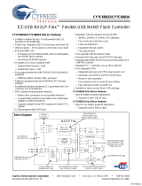
Figure 1-1. NX2LP Block Diagram
USB 2.0
Xceiver
Smart HS/
FS USB
Engine
NAND Flash
Interface
Logic
8-bit Data Bus
NAND Control Signals
EZ-USB NX2LP
Internal Control Logic
PLL
24 MHz
Xtal
VBUS
D+
D-
Data
Control
Chip Reset
LED1#
LED2#
Write Protect
Chip Enable Signals
[+] Feedback

CY7C68023/CY7C68024
Document #: 38-08055 Rev. *B Page 2 of 9
3.0 Pin Assignments
3.1 Pin Diagram
Figure 3-1. 56-pin QFN
3.2 Pin Descriptions
Pin Name Type Default State at Start-up Description
1 R_B1#
[1]
I Z Ready/Busy 1 (2.2k to 4k pull-up resistor is required)
2 R_B2# I Z Ready/Busy 2 (2.2k to 4k pull-up resistor is required)
3 AVCC PWR PWR Analog 3.3V supply
4 XTALOUT Xtal N/A Crystal output
5 XTALIN Xtal N/A Crystal input
6 AGND GND GND Ground
7 AVCC PWR PWR Analog 3.3V supply
8 DPLUS I/O Z USB D+
9 DMINUS I/O Z USB D-
10 AGND GND GND Ground
11 VCC PWR PWR 3.3V supply
12 GND GND GND Ground
13 N/C N/A N/A No connect
14 GND GND GND Ground
15 Reserved N/A N/A Must be tied HIGH (no pull-up resistor required)
Note:
1. A # sign after the pin name indicates that it is an active LOW signal.
RESET#
GND
N/C
N/C
WP_SW#
WP_NF#
LED2#
LED1#
ALE
CLE
VCC
RE1#
RE0#
WE#
R_B1#
R_B2#
AVCC
XTALOUT
XTALIN
AGND
AVCC
DPLUS
DMINUS
AGND
VCC
GND
N/C
GND
15
16
17
18
19
20
21
22
23
24
25
26
27
28
Reserved
Reserved
VCC
DD0
DD1
DD2
DD3
DD4
DD5
DD6
DD7
GND
VCC
GND
42
41
40
39
38
37
36
35
34
33
32
31
30
29
56
55
54
53
52
51
50
49
48
47
46
45
44
43
1
2
3
4
5
6
7
8
9
10
11
12
13
14
GND
VCC
N/C
GND
CE7#
CE6#
CE5#
CE4#
CE3#
CE2#
CE1#
CE0#
Reserved
VCC
EZ-USB NX2LP
56-pin QFN
[+] Feedback

CY7C68023/CY7C68024
Document #: 38-08055 Rev. *B Page 3 of 9
16 Reserved N/A N/A Must be tied HIGH (no pull-up resistor required)
17 VCC PWR PWR 3.3V supply
18 DDO I/O Z Data 0
19 DD1 I/O Z Data 1
20 DD2 I/O Z Data 2
21 DD3 I/O Z Data 3
22 DD4 I/O Z Data 4
23 DD5 I/O Z Data 5
24 DD6 I/O Z Data 6
25 DD7 I/O Z Data 7
26 GND GND GND Ground
27 VCC PWR PWR 3.3V supply
28 GND GND GND Ground
29 WE# O H Write enable
30 RE0# O H Read Enable 0
31 RE1# O H Read Enable 1
32 VCC PWR PWR 3.3V supply
33 CLE O Z Command latch enable
34 ALE O Z Address latch enable
35 LED1# O Z Data activity LED sink
36 LED2# O Z Chip active LED sink
37 WP_NF# O Z Write-protect NAND Flash
38 WP_SW# I Z Write-protect switch input
39 N/C N/A N/A No connect
40 N/C N/A N/A No connect
41 GND GND GND Ground
42 RESET# I Z NX2LP chip reset
43 VCC PWR PWR 3.3V supply
44 Reserved N/A N/A Must be tied HIGH
45 CE0# O Z Chip enable 0
46 CE1# O Z Chip enable 1
47 CE2# O Z Chip enable 2
48 CE3# O Z Chip enable 3
49 CE4# O Z Chip enable 4
50 CE5# O Z Chip enable 5
51 CE6# O Z Chip enable 6
52 CE7# O Z Chip enable 7
53 GND GND GND Ground
54 N/C N/A N/A No connect
55 VCC PWR PWR 3.3V supply
56 GND GND GND Ground
3.2 Pin Descriptions (continued)
Pin Name Type Default State at Start-up Description
[+] Feedback

CY7C68023/CY7C68024
Document #: 38-08055 Rev. *B Page 4 of 9
3.3 Additional Pin Descriptions
3.3.1 DPLUS, DMINUS
DPLUS and DMINUS are the USB signaling pins, and they
should be tied to the D+ and D– pins of the USB connector.
Because they operate at high frequencies, the USB signals
require special consideration when designing the layout of the
PCB. General guidelines are given at the end of this
document.
3.3.2 XTALIN, XTALOUT
The NX2LP requires a 24-MHz (±100 ppm) signal to derive
internal timing. Typically, a 24-MHz (20-pF, 500-µW, parallel-
resonant fundamental mode) crystal is used, but a 24-MHz
square wave from another source can also be used. If a crystal
is used, connect its pins to XTALIN and XTALOUT, and also
through 12-pF capacitors to GND. If an alternate clock source
is used, apply it to XTALIN and leave XTALOUT open.
3.3.3 Data[7-0]
The Data[7-0] I/O pins provide an 8-bit interface to a NAND
Flash device. These pins are used to transfer address,
command, and read/write data between the NX2LP and NAND
Flash.
3.3.4 R_B[2-1]#
The Ready/Busy input pins are used to determine the state of
the currently selected NAND Flash device. These pins must
be pulled HIGH through a 2k-4k resistor. These pins are pulled
LOW by the NAND Flash when it is busy.
3.3.5 WE#
The Write Enable output pin is used by the NAND Flash to
latch commands, address, and data during the rising edge of
the pulse.
3.3.6 RE[1-0]#
The Read Enable output pins are used to control the data flow
from the NAND Flash devices. The device presents valid data
and will increment its internal column address counter by one
step on each falling edge of the Read Enable pulse. A 10k pull-
up is an option For RE1-0#.
3.3.7 CLE
The Command Latch Enable output pin is used to indicate that
the data on the I/O bus is a command. The data is latched into
the NAND Flash control register on the rising edge of WE#
when CLE is HIGH.
3.3.8 ALE
The Address Latch Enable output pin is used to indicate that
the data on the I/O bus is an address. The data is latched into
the NAND Flash address register on the rising edge of WE#
when ALE is HIGH.
3.3.9 LED1#
The Data Activity LED output pin is used to indicate data
transfer activity. LED1# is asserted LOW at the beginning of a
data transfer, and set to a high-Z state when the transfer is
complete. If this functionality is not utilized, leave LED1#
floating.
3.3.10 LED2#
The Chip Active LED output pin is used to indicate proper
device operation. LED2# is asserted LOW when the NX2LP is
powered and initialized. It is placed in a high-Z state under all
other conditions. If this functionality is not utilized, leave
LED2# floating.
3.3.11 WP_NF#
The Write-protect NAND Flash output pin is used to control the
write-protect pins on NAND Flash devices. This pin should be
tied to the Write Protect pins of the NAND Flash devices. If
WP_SW# is asserted LOW during a data transfer, or if internal
operations are still pending, the NX2LP will wait until the
operation is complete before asserting WP_NF# to ensure that
there is no data loss or risk of OS error.
3.3.12 WP_SW#
The Write-protect Switch input pin is used to select whether or
not NAND Flash write-protection is enabled by the NX2LP.
When the pin is asserted LOW, the NX2LP will report to the
host that the NAND Flash is write-protected, the WP_NF# will
be driven LOW, and any attempts to write to the configuration
data memory area will be blocked by the NX2LP. If this pin is
asserted LOW during a data transfer, or if internal operations
are still pending, the NX2LP will wait until the operation is
complete before asserting WP_NF# to ensure that there is no
data loss or risk of OS error.
3.3.13 CE[7-0]#
The Chip Enable output pins are used to select the NAND
Flash that the NX2LP will interface. Unused Chip Enable pins
should be left floating.
3.3.14 RESET#
Asserting RESET# for 10 ms will reset the NX2LP. A reset
and/or watchdog chip is recommended to ensure that startup
and brownout conditions are properly handled.
Figure 3-2. XTALIN, XTALOUT Diagram
24-MHz Xtal
12 pF
XTALIN XTALOUT
12 pF
12-pF capacitor
values assume a
trace capacitance
of 3 pF per side on a
four-layer FR4 PCB
[+] Feedback

CY7C68023/CY7C68024
Document #: 38-08055 Rev. *B Page 5 of 9
4.0 Applications
The NX2LP is a high-speed USB 2.0 peripheral device that
connects NAND Flash devices to a USB host using the USB
Mass Storage Class protocol.
4.1 Additional Resources
• CY3685 EZ-USB NX2LP Development Kit
• CY4618 EZ-USB NX2LP Reference Design Kit
• USB Specification version 2.0
• USB Mass Storage Class Bulk Only Transport Specification,
http://www.usb.org/developers/data/devclass/
usbmassbulk_10.pdf.
5.0 Functional Overview
5.1 USB Signaling Speed
The NX2LP operates at two of the three rates defined in the
USB Specification Revision 2.0 dated April 27, 2000:
• Full speed, with a signaling bit rate of 12 Mbits/sec
• High speed, with a signaling bit rate of 480 Mbits/sec.
The NX2LP does not support the low-speed signaling rate of
1.5 Mbits/sec.
5.2 NAND Flash Interface
During normal operation the NX2LP supports an 8-bit I/O
interface, eight chip enable pins, and other control signals
compatible with industry standard NAND Flash devices.
6.0 Enumeration
During the start-up sequence, internal logic checks for the
presence of NAND Flash with valid configuration data in the
configuration data memory area. If valid configuration data is
found, the NX2LP uses the values stored in NAND Flash to
configure the USB descriptors for normal operation as a USB
mass storage device. If no NAND Flash is detected, or if no
valid configuration data is found in the configuration data
memory area, the NX2LP uses the default values from internal
ROM space for manufacturing mode operation. The two
modes of operation are described in sections 6.1 and 6.2
below.
6.1 Normal Operation Mode
In Normal Operation Mode, the NX2LP behaves as a USB 2.0
Mass Storage Class NAND Flash controller. This includes all
typical USB device states (powered, configured, etc.). The
USB descriptors are returned according to the data stored in
the configuration data memory area. Normal read and write
access to the NAND Flash is available in this mode.
6.2 Manufacturing Mode
In Manufacturing mode, the NX2LP enumerates using the
default descriptors and configuration data that are stored in
internal ROM. This mode allows for first-time programming of
the configuration data memory area, as well as board-level
manufacturing tests.
A unique USB serial number is required for each device in
order to comply with the USB Mass Storage specification.
Also, Cypress requires designers to use their own Vendor ID
for final products. The Vendor ID is obtained through regis-
tration with the USB Implementor’s Forum (USB-IF), and the
Product ID is determined by the designer.
Cypress provides all the software tools and drivers necessary
for properly programming and testing the NX2LP. Please refer
to the documentation in the development or reference design
kit for more information on these topics.
6.3 Configuration Data
Certain features in the NX2LP can be configured by the
designer to disable unneeded features, and to comply with the
USB 2.0 specification’s descriptor requirements for mass
storage devices. Table 6-1 lists the variable configuration data
and the default values that are stored in internal ROM space.
The default ROM values are returned by an unprogrammed
NX2LP device.
NAND Flash
Programmed?
Load Default
Descriptors and
Configuration Data
Manufacturing
Mode
Load Custom
Descriptors and
Configuration Data
Enumerate As
USB Mass
Storage Device
Normal Operation
Mode
Start-up
Enumerate As
Generic NX2LP
Device
NAND Flash
Present?
No
Yes
Yes No
Figure 6-1. NX2LP Enumeration Process
[+] Feedback

CY7C68023/CY7C68024
Document #: 38-08055 Rev. *B Page 6 of 9
7.0 Design Notes For The Quad Flat No Lead
(QFN) Package
The NX2LP comes in a 56-pin QFN package, which utilizes a
metal pad on the bottom to aid in heat dissipation. The low-
power operation of the NX2LP makes the thermal pad on the
bottom of the QFN package unnecessary. Because of this,
PCB layout may utilize the space under the NX2LP for routing
signals as needed, provided that any traces or vias under the
thermal pad are covered by solder mask or other material to
prevent shorting. Standard PCB layout recommendations for
USB devices still apply.
For further information on this package design, please refer to
the application note from AMKOR titled “Surface Mount
Assembly of AMKOR’s MicroLeadFrame (MLF) Technology.”
This application note provides detailed information on board
mounting guidelines, soldering flow, rework process, etc.
8.0 PCB Layout Recommendations
The following recommendations should be followed to ensure
reliable High-speed USB performance operation.
• A four-layer impedance controlled board is recommended
to ensure best signal quality.
• Specify impedance targets (ask your board vendor what
they can achieve).
• Maintain trace widths and trace spacing to control imped-
ance.
• Minimize stubs on DPLUS and DMINUS to avoid reflected
signals.
• Place any connections between the USB connector shell
and signal ground near the USB connector.
• Use bypass/flyback caps on VBUS, placed near connector.
• Keep DPLUS and DMINUS trace lengths to within 2 mm of
each other in length, with preferred length of 20–30 mm.
• Maintain a solid ground plane under the DPLUS and DMI-
NUS traces. Do not allow the plane to be split under these
traces.
• Place no vias on the DPLUS or DMINUS trace routing.
• Isolate the DPLUS and DMINUS traces from all other signal
traces (use >10 mm. spacing for best signal quality).
Source for recommendations:
• EZ-USB FX2 PCB Design Recommendations,
www.cy-
press.com/cfuploads/support/app_notes/FX2_PCB.pdf.
• High-speed USB Platform Design Guidelines,
www.usb.org/developers/data/hs_usb_pdg_r1_0.pdf.
9.0 Absolute Maximum Ratings
Storage Temperature...................................–65°C to +150°C
Ambient Temperature with Power
Supplied............................................................ 0°C to +70°C
Supply Voltage to Ground Potential................–0.5V to +4.0V
DC Input Voltage to Any Input Pin ................................ 5.25V
DC Voltage Applied to Outputs
in High-Z State..................................... –0.5V to VCC + 0.5V
Power Dissipation..................................................... 300 mW
Static Discharge Voltage.............................................. 2000V
Max Output Current per IO port................................... 10 mA
10.0 Operating Conditions
[2]
T
A
(Ambient Temperature Under Bias) ............. 0°C to +70°C
Supply Voltage............................................+3.00V to +3.60V
Ground Voltage.................................................................. 0V
F
OSC
(Oscillator or Crystal Frequency) ... 24 MHz ± 100 ppm
Parallel Resonant
Note:
2. If an alternate clock source is input on XTALIN, it must be supplied with standard 3.3V signaling characteristics and XTALOUT must be left floating.
Table 6-1. Variable Configuration Data And Default ROM Values
Configuration Data Description Default ROM Value
Vendor ID USB Vendor ID (Assigned by USB-IF) 0x04B4 (Cypress)
Product ID USB Product ID (Assigned by designer) 0x6813
Serial Number USB serial number N/A
Manufacturer String Manufacturer string in USB descriptors N/A
Product String Product string in USB descriptors N/A
Enable Write Protection Enables write protection capability Enabled
SCSI Device Name String shown in the device manager properties N/A
[+] Feedback

CY7C68023/CY7C68024
Document #: 38-08055 Rev. *B Page 7 of 9
12.0 AC Electrical Characteristics
12.1 USB Transceiver
The NX2LP’s USB interface complies with the USB 2.0 speci-
fication for bus-powered devices.
12.2 NAND Flash Timing
The NX2LP supports 30-ns, 50-ns, and 100-ns NAND Flash
devices.
13.0 Ordering Information
Note:
3. Measured at Max V
CC
, 25°C.
11.0 DC Characteristics
Parameter Description Conditions Min. Typ. Max. Unit
V
CC
Supply Voltage 3.0 3.3 3.6 V
V
CC
Ramp Supply Ramp-up 0V to 3.3V 200 µs
V
IH
Input High Voltage 2 5.25 V
V
IL
Input Low Voltage –0.5 0.8 V
I
I
Input Leakage Current 0 < V
IN
< V
CC
±10 µA
V
IH_X
Crystal Input HIGH Voltage 2 5.25 V
V
IL_X
Crystal Input LOW Voltage –0.5 0.8 V
V
OH
Output Voltage High I
OUT
= 4 mA 2.4 V
V
OL
Output Voltage Low I
OUT
= –4 mA 0.4 V
I
OH
Output Current High 4mA
I
OL
Output Current Low 4mA
C
IN
Input Pin Capacitance All but D+/D– 10 pF
Only D+/D– 15 pF
I
CC
Supply Current USB High Speed 50 mA
USB Full Speed 35 mA
I
SUSP
Suspend Current CY7C68023 Connected 0.5 1.2
[3]
mA
Disconnected 0.3 1.0
[3]
mA
CY7C68024 Connected 300 380
[3]
µA
Disconnected 100 150
[3]
µA
I
UNCONFIG
Unconfigured Current Before current requested in USB
descriptors is granted by the host
43 mA
T
RESET
Reset Time After Valid Power V
CC
> 3.0V 5.0 mS
Pin Reset After Valid Startup 200 µS
Part Number Package Type
CY7C68023-56LFXC 56-pin QFN Lead-free For Self/Bus Power
CY7C68024-56LFXC 56-pin QFN Lead-free For Battery Power
CY3685 EZ-USB NX2LP Development Kit
CY4618 EZ-USB NX2LP Reference Design Kit
[+] Feedback

CY7C68023/CY7C68024
Document #: 38-08055 Rev. *B Page 8 of 9
© Cypress Semiconductor Corporation, 2005. The information contained herein is subject to change without notice. Cypress Semiconductor Corporation assumes no responsibility for the use
of any circuitry other than circuitry embodied in a Cypress product. Nor does it convey or imply any license under patent or other rights. Cypress products are not warranted nor intended to be
used for medical, life support, life saving, critical control or safety applications, unless pursuant to an express written agreement with Cypress. Furthermore, Cypress does not authorize its
products for use as critical components in life-support systems where a malfunction or failure may reasonably be expected to result in significant injury to the user. The inclusion of Cypress
products in life-support systems application implies that the manufacturer assumes all risk of such use and in doing so indemnifies Cypress against all charges.
14.0 Package Diagram
15.0 Disclaimers, Trademarks, and Copyrights
EZ-USB NX2LP is a trademark, and EZ-USB is a registered trademark, of Cypress Semiconductor Corporation. All product and
company names mentioned in this document are the trademarks of their respective holders.
Figure 14-1. 56-lead Quad Flatpack No Lead (8 x 8 mm) LF56
0.80[0.031]
7.70[0.303]
7.90[0.311]
A
C
1.00[0.039] MAX.
N
SEATING
PLANE
N
2
0.18[0.007]
0.50[0.020]
1
1
0.08[0.003]
0.50[0.020]
0.05[0.002] MAX.
2
(4X)
C
0.24[0.009]
0.20[0.008] REF.
0.80[0.031] MAX.
PIN1 ID
0°-12°
6.45[0.254]
8.10[0.319]
7.80[0.307]
6.55[0.258]
0.45[0.018]
0.20[0.008] R.
8.10[0.319]
7.90[0.311]
7.80[0.307]
7.70[0.303]
DIA.
0.28[0.011]
0.30[0.012]
6.55[0.258]
6.45[0.254]
0.60[0.024]
TOP VIEW
BOTTOM VIEW
SIDE VIEW
E-PAD
(PAD SIZE VARY
BY DEVICE TYPE)
51-85144-*D
56-Lead QFN 8 x 8 MM LF56A
Dimensions in mm
E-Pad Size 4.3 x 5.0 mm (typ.)
[+] Feedback

CY7C68023/CY7C68024
Document #: 38-08055 Rev. *B Page 9 of 9
Document History Page
Description Title: CY7C68023/CY7C68024 EZ-USB NX2LP™ USB 2.0 NAND Flash Controller
Document Number: 38-08055
REV. ECN NO.
Issue
Date
Orig. of
Change Description of Change
** 286009 SEE ECN GIR New Data Sheet (Preliminary Information).
*A 334796 SEE ECN GIR Adjusted default VID/PID; released as final.
*B 397024 SEE ECN GIR Changed Vcc to ±10% in DC Characteristics table. Changed the supply
voltage tolerance to ±10% in the Operating Conditions section. Added new
logo.
[+] Feedback
/