Page is loading ...

EZ-USB AT2LP™ USB 2.0 to ATA/ATAPI Bridge
CY7C68300C/CY7C68301C
CY7C68320C/CY7C68321C
Cypress Semiconductor Corporation • 198 Champion Court • San Jose, CA 95134-1709 • 408-943-2600
Document 001-05809 Rev. *A Revised November 30, 2006
Features
• Fixed-function mass storage device—requires no firmware
• Two power modes: Self-powered and USB bus-powered to
enable bus powered CF readers and truly portable USB
hard drives
• Certified compliant for USB 2.0 (TID# 40490119), the USB
Mass Storage Class, and the USB Mass Storage Class
Bulk-Only Transport (BOT) Specification
• Operates at high-speed (480 Mbps) or full-speed (12 Mbps)
USB
• Complies with ATA/ATAPI-6 specification
• Supports 48 bit addressing for large hard drives
• Supports ATA security features
• Supports any ATA command with the ATACB function
• Supports mode page 5 for BIOS boot support
• Supports ATAPI serial number VPD page retrieval for Digital
Rights Management (DRM) compatibility
• Supports PIO modes 0, 3, and 4, multiword DMA mode 2,
and UDMA modes 2, 3, and 4
• Uses one small external serial EEPROM for storage of USB
descriptors and device configuration data
• ATA interface IRQ signal support
• Supports one or two ATA/ATAPI devices
• Supports CompactFlash and one ATA/ATAPI device
• Supports board-level manufacturing test using the USB I/F
• Can place the ATA interface in high impedance (Hi-Z) to
allow sharing of the ATA bus with another controller (i.e., an
IEEE-1394 to ATA bridge chip or MP3 Decoder)
• Low-power 3.3V operation
• Fully compatible with native USB mass storage class drivers
• Cypress mass storage class drivers available for Windows
(98SE, ME, 2000, XP) and Mac OS X operating systems
Features (CY7C68320C/CY7C68321C only)
• Supports HID interface or custom GPIOs to enable features
such as single button backup, power-off, LED-based notifi-
cation, etc.
• 56-pin QFN and 100-pin TQFP lead-free packages
• CY7C68321C is ideal for battery-powered designs
• CY7C68320C is ideal for self- and bus-powered designs
Features (CY7C68300C/CY7C68301C only)
• Pin-compatible with CY7C68300A (using Backward
Compatibility mode)
• 56-pin SSOP and 56-pin QFN lead-free packages
• CY7C68301C is ideal for battery-powered designs
• CY7C68300C is ideal for self- and bus-powered designs
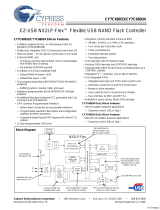
USB 2.0
Tranceiver
CY Smart USB
FS/HS Engine
4 kByte FIFO
PLL
I
2
C Bus Master
ATA
Interface
Logic
Data
Control
24
MHz
XTAL
16 Bit ATA DataUSB
D+
D-
Internal Control Logic
VBUS
ATA Interface
Control Signals
Misc control signals and GPIO
SDA
SCL
ATA 3-state Control
Reset
Block Diagram
[+] Feedback

CY7C68300C/CY7C68301C
CY7C68320C/CY7C68321C
Document 001-05809 Rev. *A Page 2 of 42
Applications
The CY7C68300C/301C and CY7C68320C/321A implement
a USB 2.0 bridge for all ATA/ATAPI-6 compliant mass storage
devices, such as the following:
• Hard drives
• CD-ROM, CD-R/W
• DVD-ROM, DVD-RAM, DVD±R/W
• MP3 players
• Personal media players
• CompactFlash
• Microdrives
• Tape drives
• Personal video recorders
The CY7C68300C/301C and CY7C68320C/321A support one
or two devices in the following configurations:
• ATA/ATAPI master only
• ATA/ATAPI slave only
• ATA/ATAPI master and ATA/ATAPI slave
• CompactFlash only
• ATA/ATAPI slave and CompactFlash or other removable
IDE master
Additional Resources
• CY4615C EZ-USB AT2LP Reference Design Kit
• USB Specification version 2.0
• ATA Specification T13/1410D Rev 3B
• USB Mass Storage Class Bulk Only Transport Specification,
www.usb.org
Introduction
The EZ-USB AT2LP™ (CY7C68300C/CY7C68301C and
CY7C68320C/CY7C68321C) implements a fixed-function
bridge between one USB port and one or two ATA- or
ATAPI-based mass storage device ports. This bridge adheres
to the Mass Storage Class Bulk-Only Transport Specification
(BOT) and is intended for bus- and self-powered devices.
The AT2LP is the latest addition to the Cypress USB mass
storage portfolio, and is an ideal cost- and power-reduction
path for designs that previously used Cypress’s ISD-300A1,
ISD-300LP, or EZ-USB AT2.
Specifically, the CY7C68300C/CY7C68301C includes a
mode that makes it pin-for-pin compatible with the
EZ-USB AT2 (CY7C68300A).
The USB port of the CY7C68300C/301C and
CY7C68320C/321A (AT2LP) are connected to a host
computer directly or with the downstream port of a USB hub.
Software on the USB host system issues commands and
sends data to the AT2LP and receives status and data from
the AT2LP using standard USB protocol.
The ATA/ATAPI port of the AT2LP is connected to one or two
mass storage devices. A 4 KB buffer maximizes ATA/ATAPI
data transfer rates by minimizing losses due to device seek
times. The ATA interface supports ATA PIO modes 0, 3, and 4,
multiword DMA mode 2, and Ultra DMA modes 2, 3, and 4.
The device initialization process is configurable, enabling the
AT2LP to initialize ATA/ATAPI devices without software inter-
vention.
CY7C68300A Compatibility
As mentioned above, the CY7C68300C/301C contains a
backward compatibility mode that allows it to be used in
existing EZ-USB AT2 (CY7C68300A) designs. The backward
compatibility mode is enabled by programming the EEPROM
with the CY7C68300A signature.
During startup, the AT2LP checks the I
2
C™ bus for an
EEPROM with a valid signature in the first two bytes. If the
signature is 0x4D4D, the AT2LP configures itself for pin-to-pin
compatibility with the AT2 and begins normal mass storage
operation. If the signature is 0x534B, the AT2LP configures
itself with the AT2LP pinout and begins normal mass storage
operation.
Refer to the logic flow in Figure 1 for more information on the
pinout selection process.
Most designs that use the AT2 can migrate to the AT2LP with
no changes to either the board layout or EEPROM data.
Cypress has published an application note focused on
migrating from the AT2 to the AT2LP to help expedite the
process. It can be downloaded from the Cypress website
(http://www.cypress.com) or obtained through a Cypress
representative.
Figure 1. Simplified Pinout Selection Flowchart
Read EEPROM
EEPROM
Signature
0x4D4D?
Yes
Set
EZ-USB AT2
(CY7C68300A)
Pinout
Set
EZ-USB AT2LP
(CY7C68300B)
Pinout
No
Normal Operation
[+] Feedback

CY7C68300C/CY7C68301C
CY7C68320C/CY7C68321C
Document 001-05809 Rev. *A Page 3 of 42
Pin Diagrams
The AT2LP is available in different package types to meet a variety of design needs. The CY7C68320C/321C is available in 56-pin
QFN and 100-pin TQFP packages to provide the greatest flexibility for new designs. The CY7C68300C/301C is available in 56-pin
SSOP and QFN package types to ensure backward compatibility with CY7C68300A designs.
Figure 2. 56-pin SSOP Pinout (CY7C68300C/CY7C68301C only)
5
6
7
8
9
10
11
12
13
14
15
16
17
18
19
20
21
22
23
24
25
26
27
28
1
2
3
4
52
51
50
49
48
47
46
45
44
43
42
41
40
39
38
37
36
35
34
33
32
31
30
29
56
55
54
53
ATAPUEN (GND)
VCC
GND
IORDY
DMARQ
AVCC
XTALOUT
XTALIN
AGND
VCC
DPLUS
DMINUS
GND
VCC
GND
PWR500# (PU 10K)
GND (Reserved)
SCL
SDA
VCC
DD0
DD1
DD2
DD3
DD13
DD14
DD15
GND
EZ-USB AT2LP
CY7C68300C
CY7C68301C
56-pin SSOP
DD8
(ATA_EN) VBUS_ATA_ENABLE
VCC
RESET#
GND
ARESET#
(VBUS_PWR_VALID) DA2
CS1#
CS0#
(DA2) DRVPWRVLD
DA1
DA0
INTRQ
VCC
DMACK#
DIOR#
DIOW#
GND
VCC
GND
DD7
DD6
DD5
DD4
DD12
DD11
DD10
DD9
NOTE: Labels in italics denote pin functionality
during CY7C68300A compatibility mode.
[+] Feedback

CY7C68300C/CY7C68301C
CY7C68320C/CY7C68321C
Document 001-05809 Rev. *A Page 4 of 42
Figure 3. 56-pin QFN Pinout (CY7C68300C/CY7C68301C)
RESET#
GND
ARESET#
DA2 (VBUS_PWR_VALID)
CS1#
CS0#
DRVPWRVLD (DA2)
DA1
DA0
INTRQ
VCC
DMACK#
DIOR#
DIOW#
IORDY
DMARQ
AVCC
XTALOUT
XTALIN
AGND
VCC
DPLUS
DMINUS
GND
VCC
GND
(PU10K) PWR500#
GND
15
16
17
18
19
20
21
22
23
24
25
26
27
28
SCL
SDA
VCC
DD0
DD1
DD2
DD3
DD4
DD5
DD6
DD7
GND
VCC
GND
42
41
40
39
38
37
36
35
34
33
32
31
30
29
56
55
54
53
52
51
50
49
48
47
46
45
44
43
1
2
3
4
5
6
7
8
9
10
11
12
13
14
GND
VCC
ATAPUEN (NC)
GND
DD15
DD14
DD13
DD12
DD11
DD10
DD9
DD8
VBUS_ATA_ENABLE (ATA_EN)
VCC
EZ-USB AT2LP
CY7C68300C
CY7C68301C
56-pin QFN
NOTE: Italic labels denote pin functionality
during CY7C68300A compatibility mode.
[+] Feedback

CY7C68300C/CY7C68301C
CY7C68320C/CY7C68321C
Document 001-05809 Rev. *A Page 5 of 42
Figure 4. 56-pin SSOP Pinout (CY7C68320C/CY7C68321C)
5
6
7
8
9
10
11
12
13
14
15
16
17
18
19
20
21
22
23
24
25
26
27
28
1
2
3
4
52
51
50
49
48
47
46
45
44
43
42
41
40
39
38
37
36
35
34
33
32
31
30
29
56
55
54
53
GPIO2
VCC
GND
IORDY
DMARQ
AVCC
XTALOUT
XTALIN
AGND
VCC
DPLUS
DMINUS
GND
VCC
GND
GPIO1
GND
SCL
SDA
VCC
DD0
DD1
DD2
DD3
DD13
DD14
DD15
GND
EZ-USB AT2LP
CY7C68320C
CY7C68321C
56-pin SSOP
DD8
VBUS_ATA_ENABLE
VCC
RESET#
GND
ARESET#
DA2
CS1#
CS0#
GPIO0
DA1
DA0
INTRQ
VCC
DMACK#
DIOR#
DIOW#
GND
VCC
GND
DD7
DD6
DD5
DD4
DD12
DD11
DD10
DD9
[+] Feedback

CY7C68300C/CY7C68301C
CY7C68320C/CY7C68321C
Document 001-05809 Rev. *A Page 6 of 42
Figure 5. 56-pin QFN Pinout (CY7C68320C/CY7C68321C)
GND
VCC
GPIO2
GND
DD15
DD14
DD13
DD12
DD11
DD10
DD9
DD8
VBUS_ATA_ENABLE
VCC
RESET#
GND
ARESET#
DA2
CS1#
CS0#
GPIO0
DA1
DA0
INTRQ
VCC
DMACK#
DIOR#
DIOW#
IORDY
DMARQ
AVCC
XTALOUT
XTALIN
AGND
VCC
DPLUS
DMINUS
GND
VCC
GND
GPIO1
GND
SCL
SDA
VCC
DD0
DD1
DD2
DD3
DD4
DD5
DD6
DD7
GND
VCC
GND
15
16
17
18
19
20
21
22
23
24
25
26
27
28
42
41
40
39
38
37
36
35
34
33
32
31
30
29
56
55
54
53
52
51
50
49
48
47
46
45
44
43
1
2
3
4
5
6
7
8
9
10
11
12
13
14
EZ-USB AT2LP
CY7C68320C
CY7C68321C
56-pin QFN
[+] Feedback

CY7C68300C/CY7C68301C
CY7C68320C/CY7C68321C
Document 001-05809 Rev. *A Page 7 of 42
Figure 6. 100-pin TQFP Pinout (CY7C68320C/CY7C68321C only)
100
99
98
97
96
95
94
93
92
91
90
89
88
87
86
85
84
83
82
81
1
2
3
4
5
6
7
8
9
10
11
12
13
14
15
16
17
18
19
20
21
22
23
24
25
26
27
28
29
30
DD8
VBUS_ATA_ENABLE
VCC
RESET#
NC
GND
ARESET#
DA2
CS1#
CS0#
DRVPWRVLD
DA1
DA0
INTRQ
VCC
GND
NC
NC
VBUSPWRD
NC
NC
NC
LOWPWR#
NC
DMACK#
DIOR#
DIOW#
VCC
NC
NC
VCC
GND
IORDY
DMARQ
GND
GND
GND
GND
AVCC
XTALOUT
XTALIN
AGND
NC
NC
NC
VCC
DPLUS
DMINUS
GND
VCC
GND
SYSIRQ
GND
GND
GND
PWR500#
GND
NC
SCL
SDA
80
79
78
77
76
75
74
73
72
71
70
69
68
67
66
65
64
63
62
61
60
59
58
57
56
55
54
53
52
51
31
32
33
34
35
36
37
38
39
40
41
42
43
44
45
46
47
48
49
50
EZ-USB AT2LP
CY7C68320A
CY7C68321A
100-pin TQFP
NC
NC
VCC
DD0
DD1
DD2
DD3
VCC
GND
NC
GND
NC
GND
DD4
DD5
DD6
DD7
GND
VCC
GND
ATAPUEN
GND
DD15
DD14
DD13
DD12
GND
GPIO5
GPIO4
GPIO3
GPIO2
GPIO1
GPIO0
NC
NC
VCC
GND
DD11
DD10
DD9
C
C
[+] Feedback

CY7C68300C/CY7C68301C
CY7C68320C/CY7C68321C
Document 001-05809 Rev. *A Page 8 of 42
Pin Descriptions
The following table lists the pinouts for the 56-pin SSOP, 56-pin
QFN and 100-pin TQFP package options for the AT2LP. Refer
to the “Pin Diagrams” on page 3 for differences between the
68300C/01C and 68320C/321C pinouts for the 56-pin
packages. For information on the CY7C68300A pinout, refer
to the CY7C68300A data sheet that is found in the ’EZ-USB
AT2’ folder of the CY4615C reference design kit CD.
Table 1. AT2LP Pin Descriptions
Note: (Italic pin names denote pin functionality during CY7C68300A compatibility mode)
100
TQFP
56
QFN
56
SSOP
Pin Name
Pin
Type
Default State
at Startup
Pin Description
1 55 6 V
CC
PWR V
CC
. Connect to 3.3V power source.
2 56 7 GND GND Ground.
3 1 8 IORDY I
[1]
Input ATA control. Apply a 1k pull up to 3.3V.
4 2 9 DMARQ I
[1]
Input ATA control.
5
6
7
8
N/A N/A GND Ground.
9 3 10 AV
CC
PWR Analog V
CC
. Connect to V
CC
through the shortest path
possible.
10 4 11 XTALOUT Xtal Xtal 24 MHz crystal output. (See “XTALIN, XTALOUT” on
page 11).
11 5 12 XTALIN Xtal Xtal 24 MHz crystal input. (See “XTALIN, XTALOUT” on
page 11).
12 6 13 AGND GND Analog ground. Connect to ground with as short a
path as possible.
13
14
15
N/A N/A NC No connect.
16 7 14 V
CC
PWR V
CC
. Connect to 3.3V power source.
17 8 15 DPLUS IO Hi-Z USB D+ signal (See “DPLUS, DMINUS” on page 11).
18 9 16 DMINUS IO Hi-Z USB D–signal (See “DPLUS, DMINUS” on page 11).
19 10 17 GND GND Ground.
20 11 18 V
CC
PWR V
CC
. Connect to 3.3V power source.
21 12 19 GND GND Ground.
22 N/A N/A SYSIRQ I Input USB interrupt request. (See “SYSIRQ” on page 12).
Active HIGH. Connect to GND if functionality is not
used.
23
24
25
N/A N/A GND GND Ground.
26
[3]
13
[3]
20 PWR500#
[2]
(PU 10K)
O bMaxPower request granted indicator. (See
“PWR500#” on page 14). Active LOW.
N/A for CY7C68320C/CY7C68321C 56-pin packages.
27 14 21 GND (RESERVED) Reserved. Tie to GND.
28 N/A N/A NC No connect.
29 15 22 SCL O Active for
several ms at
startup.
Clock signal for I
2
C interface. (See “SCL, SDA” on
page 11). Apply a 2.2k pull up resistor.
Notes
1. If byte 8, bit 4 of the EEPROM is set to ‘0’, the ATA interface pins are only active when VBUS_ATA_EN is asserted. See
“VBUS_ATA_ENABLE” on
page 14
.
2. A ‘#’ sign after the pin name indicates that it is active LOW.
[+] Feedback

CY7C68300C/CY7C68301C
CY7C68320C/CY7C68321C
Document 001-05809 Rev. *A Page 9 of 42
30 16 23 SDA IO Data signal for I
2
C interface. (See “SCL, SDA” on
page 11).
Apply a 2.2k pull up resistor.
31
32
N/A N/A NC No connect.
33 17 24 V
CC
PWR V
CC
. Connect to 3.3V power source.
34 18 25 DD0 IO
[1]
Hi-Z ATA data bit 0.
35 19 26 DD1 IO
[1]
Hi-Z ATA data bit 1.
36 20 27 DD2 IO
[1]
Hi-Z ATA data bit 2.
37 21 28 DD3 IO
[1]
Hi-Z ATA data bit 3.
38 N/A N/A V
CC
PWR V
CC
. Connect to 3.3V power source.
39 N/A N/A GND GND Ground.
40 N/A N/A NC NC No connect.
41 N/A N/A GND Ground.
42 N/A N/A NC NC No connect.
43 N/A N/A GND Ground.
44 22 29 DD4 IO
[1]
Hi-Z ATA data bit 4.
45 23 30 DD5 IO
[1]
Hi-Z ATA data bit 5.
46 24 31 DD6 IO
[1]
Hi-Z ATA data bit 6.
47 25 32 DD7 IO
[1]
Hi-Z ATA data bit 7. Apply a 1k pull down to GND.
48 26 33 GND GND Ground.
49 27 34 V
CC
PWR V
CC
. Connect to 3.3V power source.
50 28 35 GND GND Ground.
51
52
N/A N/A NC NC No connect.
53 N/A N/A V
CC
PWR V
CC
. Connect to 3.3V power source.
54 29 36 DIOW#
[2]
O/Z
[1]
Driven HIGH
(CMOS)
ATA control.
55 30 37 DIOR# O/Z
[1]
Driven HIGH
(CMOS)
ATA control.
56 31 38 DMACK# O/Z
[1]
Driven HIGH
(CMOS)
ATA control.
57 N/A N/A NC NC No connect.
58 N/A N/A LOWPWR# O USB suspend indicator. (See “LOWPWR#” on
page 13).
59
60
61
N/A N/A NC NC No connect.
62 N/A N/A VBUSPWRD I Input Bus-powered mode selector. (See “VBUSPWRD” on
page 14).
63
64
N/A N/A NC NC No connect.
65 N/A N/A GND GND Ground.
66 32 39 V
CC
PWR V
CC
. Connect to 3.3V power source.
67 33 40 INTRQ I
[1]
Input ATA interrupt request.
Table 1. AT2LP Pin Descriptions
Note: (Italic pin names denote pin functionality during CY7C68300A compatibility mode) (continued)
100
TQFP
56
QFN
56
SSOP
Pin Name
Pin
Type
Default State
at Startup
Pin Description
[+] Feedback

CY7C68300C/CY7C68301C
CY7C68320C/CY7C68321C
Document 001-05809 Rev. *A Page 10 of 42
68 34 41 DA0 O/Z
[1]
Driven HIGH
after 2 ms
delay
ATA address.
69 35 42 DA1 O/Z
[1]
Driven HIGH
after 2 ms
delay
ATA address.
70
[3]
36
[3]
43 DRVPWRVLD
(DA2)
I Input Device presence detect. (See “DRVPWRVLD” on
page 13). Configurable logical polarity is controlled by
EEPROM address 0x08. This pin must be pulled HIGH
if functionality is not utilized.
Alternate function. Input when the EEPROM configu-
ration byte 8 has bit 7 set to one. The input value is
reported through EP1IN (byte 0, bit 0).
71 37 44 CS0# O/Z
[1]
Driven HIGH
after 2 ms
delay
ATA chip select.
72 38 45 CS1# O/Z
[1]
Driven HIGH
after 2 ms
delay
ATA chip select.
73 39 46 DA2
(VBUS_PWR_VALID)
O/Z
[1]
Driven HIGH
after 2 ms
delay
ATA address.
74 40 47 ARESET# O/Z
[1]
ATA reset.
75 41 48 GND GND Ground.
76 N/A N/A NC NC No connect.
77 42 49 RESET# I Input Chip reset (See “RESET#” on page 14).
78 43 50 V
CC
PWR V
CC
. Connect to 3.3V power source.
79 44 51 VBUS_ATA_ENABLE
(ATA_EN)
I Input VBUS detection (See “VBUS_ATA_ENABLE” on
page 14).
80 45 52 DD8 IO
[1]
Hi-Z ATA data bit 8.
81 46 53 DD9 IO
[1]
Hi-Z ATA data bit 9.
82 47 54 DD10 IO
[1]
Hi-Z ATA data bit 10.
83 48 55 DD11 IO
[1]
Hi-Z ATA data bit 11.
84 N/A N/A GND Ground.
85 N/A N/A V
CC
PWR V
CC
. Connect to 3.3V power source.
86
87
N/A N/A NC NC No connect.
88
89
90
91
92
93
36
[3]
13
[3]
54
[3]
N/A GPIO0
GPIO1
GPIO2
GPIO3
GPIO4
GPIO5
IO
[3]
General purpose IO pins (See “GPIO Pins” on
page 13). The GPIO pins must be tied to GND if
functionality is not used.
94 N/A N/A GND GND Ground.
95 49 56 DD12 IO
[1]
Hi-Z ATA data bit 12.
96 50 1 DD13 IO
[1]
Hi-Z ATA data bit 13.
97 51 2 DD14 IO
[1]
Hi-Z ATA data bit 14.
98 52 3 DD15 IO
[1]
Hi-Z ATA data bit 15.
99 53 4 GND GND Ground.
Table 1. AT2LP Pin Descriptions
Note: (Italic pin names denote pin functionality during CY7C68300A compatibility mode) (continued)
100
TQFP
56
QFN
56
SSOP
Pin Name
Pin
Type
Default State
at Startup
Pin Description
[+] Feedback

CY7C68300C/CY7C68301C
CY7C68320C/CY7C68321C
Document 001-05809 Rev. *A Page 11 of 42
Additional Pin Descriptions
The following sections provide additional pin information.
DPLUS, DMINUS
DPLUS and DMINUS are the USB signaling pins; they must
be tied to the D+ and D– pins of the USB connector. Because
they operate at high frequencies, the USB signals require
special consideration when designing the layout of the PCB.
See “General PCB Layout Recommendations For USB Mass
Storage Designs” on page 39 for PCB layout recommenda-
tions.
When RESET# is released, the assertion of the internal pull
up on D+ is gated by a combination of the state of the
VBUS_ATA_ENABLE pin, the value of configuration address
0x08 bit 0 (DRVPWRVLD Enable), and the detection of a
non-removable ATA/ATAPI drive on the IDE bus. See Tab le 2
for a description of this relationship.
SCL, SDA
The clock and data pins for the I
2
C port must be connected to
the configuration EEPROM and to 2.2K pull up resistors tied
to V
CC
. If no EEPROM is used in the design, the SCL and SDA
pins must still be connected to pull up resistors. The SCL and
SDA pins are active for several milliseconds at startup.
XTALIN, XTALOUT
The AT2LP requires a 24 MHz (
±100 ppm) signal to derive
internal timing. Typically, a 24 MHz (12 pF, 500 μW,
parallel-resonant, fundamental mode) crystal is used, but a 24
MHz square wave (3.3V, 50/50 duty cycle) from another
source can also be used. If a crystal is used, connect its pins
to XTALIN and XTALOUT, and also through 12 pF capacitors
to GND as shown in Figure 7. If an alternate clock source is
used, apply it to XTALIN and leave XTALOUT unconnected.
Figure 7. XTALIN/XTALOUT Diagram
100
[3]
54
[3]
5 ATAPUEN
(NC)
IO Bus-powered ATA pull up voltage source (see
“ATAPUEN” on page 14).
Alternate function: General purpose input when the
EEPROM configuration byte 8 has bit 7 set to ‘1’. The
input value is reported through EP1IN (byte 0, bit 2).
Table 1. AT2LP Pin Descriptions
Note: (Italic pin names denote pin functionality during CY7C68300A compatibility mode) (continued)
100
TQFP
56
QFN
56
SSOP
Pin Name
Pin
Type
Default State
at Startup
Pin Description
Table 2. D+ Pull Up Assertion Dependencies
VBUS_ATA_EN111100
DRVPWRVLD Enable Bit110011
ATA/ATAPI Drive Detected
YesNoYesNoYesNo
State of D+ pull up111000
24MHz Xtal
12pF
XTALIN XTALOUT
12pF
[+] Feedback

CY7C68300C/CY7C68301C
CY7C68320C/CY7C68321C
Document 001-05809 Rev. *A Page 12 of 42
SYSIRQ
The SYSIRQ pin provides a way for systems to request service
from host software by using the USB Interrupt pipe on endpoint
1 (EP1). If the AT2LP has no pending interrupt data to return,
USB interrupt pipe data requests are NAKed. If pending data
is available, the AT2LP returns 16 bits of data. This data
indicates whether AT2LP is operating in high-speed or
full-speed, whether the AT2LP is reporting self-powered or
bus-powered operation, and the states of any GPIO pins that
are configured as inputs. GPIO pins can be individually set as
inputs or outputs, with byte 0x09 of the configuration data. The
state of any GPIO pin that is not set as an input is reported as
‘0’ in the EP1 data.
Table 3 gives the bitmap for the data returned on the interrupt
pipe and Figure 8 depicts the latching algorithm incorporated
by the AT2LP.
The SYSIRQ pin must be pulled LOW if HID functionality is
used. Refer to “HID Functions for Button Controls” on page 15
for more details on HID functionality.
Table 3. Interrupt Data Bitmap
EP1 Data Byte 1 EP1 Data Byte 0
7654321076543210
RESERVED
RESERVED
RESERVED
RESERVED
RESERVED
RESERVED
USB High-Speed
VBUS Powered
RESERVED
RESERVED
GPIO[5]
GPIO[4]
GPIO[3]
GPIO[2]
GPIO[1]
GPIO[0]
[+] Feedback

CY7C68300C/CY7C68301C
CY7C68320C/CY7C68321C
Document 001-05809 Rev. *A Page 13 of 42
Figure 8. SYSIRQ Latching Algorithm
DRVPWRVLD
When this pin is enabled with bit 0 of configuration address
0x08 (DRVPWRVLD Enable), the AT2LP informs the host that
a removable device, such as a CF card, is present. The AT2LP
uses DRVPWRVLD to detect that the removable device is
present. Pin polarity is controlled by bit 1 of configuration
address 0x08. When DRVPWRVLD is deasserted, the AT2LP
reports a “no media present” status (ASC = 0x3A, ASQ = 0x00)
when queried by the host. When the media has been detected
again, the AT2LP reports a “media changed” status to the host
(ASC = 0x28, ASQ = 0x00) when queried.
When a removable device is used, it is always considered by
the AT2LP to be the IDE master device. Only one removable
device may be attached to the AT2LP. If the system only
contains a removable device, bit 6 of configuration address
0x08 (Search ATA Bus) must be set to ‘0’ to disable ATA device
detection at startup. If a non-removable device is connected in
addition to a removable media device, the non-removable
device must be configured as IDE slave (device address 1).
GPIO Pins
The GPIO pins allow for a general purpose input and output
interface. There are several different interfaces to the GPIO
pins:
• Configuration bytes 0x09 and 0x0A contain the default
settings for the GPIO pins upon initial AT2LP configuration.
• The host can modify the settings of the GPIO pins during
operation. This is done with vendor-specific commands
described in “Programming the EEPROM” on page 33.
• The status of the GPIO pins is returned on the interrupt
endpoint (EP1) in response to a SYSIRQ. See “SYSIRQ”
on page 12 for SYSIRQ details.
LOWPWR#
LOWPWR# is an output pin that is driven to ‘0’ when the
AT2LP is not in suspend. LOWPWR# is placed in Hi-Z when
the AT2LP is in a suspend state. This pin only indicates the
state of the AT2LP and must not be used to determine the
status of the USB host because of variations in the behavior
of different hosts.
ATA Interface Pins
The ATA Interface pins must be connected to the corre-
sponding pins on an IDE connector or mass storage device.
To allow sharing of the IDE bus with other master devices, the
AT2LP can place all ATA Interface Pins in a Hi-Z state
whenever VBUS_ATA_ENABLE is not asserted. Enabling this
feature is done by setting bit 4 of configuration address 0x08
to ‘1’. Otherwise, the ATA bus is driven by the AT2LP to a
default inactive state whenever VBUS_ATA_ENABLE is not
asserted.
Design practices for signal integrity as outlined in the
ATA/ATAPI-6 specification must be followed with systems that
utilize a ribbon cable interconnect between the AT2LP’s ATA
USB Interrupt
Pipe Polled?
Yes
No
NAK Request
SYSIRQ=1?
Latch State of IO Pins
Set Int_Data = 1
Int_Data = 1?
No
Return Interrupt Data
Set Int_Data = 0
Yes
Yes
No
Yes
Int_Data = 0
and
SYSIRQ=0?
No
[+] Feedback

CY7C68300C/CY7C68301C
CY7C68320C/CY7C68321C
Document 001-05809 Rev. *A Page 14 of 42
interface and the attached mass storage device, especially if
Ultra DMA Mode is used.
VBUS_ATA_ENABLE
VBUS_ATA_ENABLE is typically used to indicate to the
AT2LP that power is present on VBUS. This pin is polled by
the AT2LP at startup and then every 20 ms thereafter. If this
pin is ‘0’, the AT2LP releases the pull up on D+ as required by
the USB specification.
Also, if bit 4 of configuration address 0x08 is ‘1’, the ATA
interface pins are placed in a Hi-Z state when
VBUS_ATA_ENABLE is ‘0’. If bit 4 of configuration address
0x08 is ‘0’, the ATA interface pins are still driven when
VBUS_ATA_ENABLE is ‘0’.
ATAPUEN
This output can be used to control the required host pull up
resistors on the ATA interface in a bus-powered design to
minimize unnecessary power consumption when the AT2LP is
in suspend. ATAPUEN is driven to ‘0’ when the ATA bus is
inactive. ATAPUEN is driven to ‘1’ when the ATA bus is active.
ATAPUEN is set to a Hi-Z state along with all other ATA
interface pins if VBUS_ATA_ENABLE is deasserted and the
ATA_EN functionality (bit 4 of configuration address 0x08) is
enabled (0).
ATAPUEN can also be configured as a GPIO input. See “HID
Functions for Button Controls” on page 15 for more infor-
mation on HID functionality.
PWR500#
The AT2LP asserts PWR500# to indicate that VBUS current
may be drawn up to the limit specified by the bMaxPower field
of the USB configuration descriptors. If the AT2LP enters a
low-power state, PWR500# is deasserted. When normal
operation is resumed, PWR500# is restored. The PWR500#
pin must never be used to control power sources for the
AT2LP. In the 56-pin package, PWR500# only functions during
bus-powered operation.
PWR500# can also be configured as a GPIO input. See “HID
Functions for Button Controls” on page 15 for more infor-
mation on HID functionality.
VBUSPWRD
VBUSPWRD is used to indicate self- or bus-powered
operation. Some designs require the ability to operate in either
self- or bus-powered modes. The VBUSPWRD input pin
enables these devices to switch between self-powered and
bus-powered modes by changing the contents of the
bMaxPower field and the self-powered bit in the reported
configuration descriptors (see Table 4).
Note that current USB host drivers do not poll the device for
this information, so the effect of this pin is only seen on a USB
or power on reset.
RESET#
Asserting RESET# for 10 ms resets the entire AT2LP. In
self-powered designs, this pin is normally tied to V
CC
through
a 100k resistor, and to GND through a 0.1 μF capacitor, as
shown in Figure 9.
Cypress does not recommend an RC reset circuit for
bus-powered devices because of the potential for VBUS
voltage drop, which may result in a startup time that exceeds
the USB limit. Refer to the application note titled EZ-USB
FX2™/AT2™/SX2™ Reset and Power Considerations, at
www.cypress.com, for more information.
While the AT2LP is in reset, all pins are held at their default
startup state.
Table 4. Behavior of Descriptor Data that is Dependent Upon VBUSPWRD State
Pin VBUSPWRD = ‘1’ VBUSPWRD = ‘0’ VBUSPWRD N/A (56-pin)
bMaxPower
Reported Value
0xFA
(500 mA)
0x01
(2 mA)
The value from configuration
address 0x34 is used.
bmAttributes bit 6
Reported Value
‘0’
(bus-powered)
‘1’
(self-powered)
‘0’ if bMaxPower > 0x01
‘1’ if bMaxPower ≤ 0x01
Figure 9. R/C Reset Circuit for Self-powered Designs
100KΩ
0.1μF
RESET#
[+] Feedback

CY7C68300C/CY7C68301C
CY7C68320C/CY7C68321C
Document 001-05809 Rev. *A Page 15 of 42
HID Functions for Button Controls
Cypress’s CY7C68320C/CY7C68321C has the capability of
supporting Human Interface Device (HID) signaling to the
host.
If there is a HID descriptor in the configuration data, the GPIO
pins that are set as inputs are polled by the AT2LP logic
approximately every 17 ms (depending on other internal
interrupt routines). If a change is detected in the state of any
HID-enabled GPIO, an HID report is sent through EP1 to the
host. The report format for byte 0 and byte 1 are shown in
Table 5.
The ability to add buttons to a mass storage solution opens
new applications for data backup and other device-side notifi-
cation to the host. The AT2LP Blaster software, found in the
CY4615C files, provides an easy way to enable and modify the
HID features of the AT2LP.
GPIO pins can be individually set as inputs or outputs, with
byte 0x09 of the configuration data, allowing for a mix of HID
and general purpose outputs. GPIOs that are not configured
as inputs are reported with a value of ‘0’ in the HID data. The
RESERVED bits’ values must be ignored, and Cypress recom-
mends using a bitmask in software to filter out unused HID
data.
Note that if using the 56-pin package, the reported GPIO[5:3]
values must be ignored because the pins are not actually
present.
Functional Overview
Chip functionally is described in the subsequent sections.
USB Signaling Speed
AT2LP operates at the following two rates defined in the USB
Specification Revision 2.0 dated April 27, 2000:
• Full-speed, with a signaling bit rate of 12 Mbits/sec.
• High-speed, with a signaling bit rate of 480 Mbits/sec.
AT2LP does not operate at the low-speed signaling rate of 1.5
Mbits/sec.
ATA Interface
The ATA/ATAPI port on the AT2LP is compatible with the Infor-
mation Technology–AT Attachment with Packet Interface–6
(ATA/ATAPI-6) Specification, T13/1410D Rev 2a. The AT2LP
supports both ATAPI packet commands as well as ATA
commands (by use of ATA Command Blocks), as outlined in
“ATA Command Block (ATACB)” on page 15. Refer to the USB
Mass Storage Class (MSC) Bulk Only Transport (BOT) Speci-
fication for information on Command Block formatting.
Additionally, the AT2LP translates ATAPI SFF-8070i
commands to ATA commands for seamless integration of ATA
devices with generic Mass Storage Class BOT drivers.
ATA Command Block (ATACB)
The ATA Command Block (ATACB) functionality provides a
means of passing ATA commands and ATA register accesses
to the attached device for execution. ATACB commands are
transferred in the Command Block Wrapper Command Block
(CBWCB) portion of the Command Block Wrapper (CBW).
The ATACB is distinguished from other command blocks by
having the first two bytes of the command block match the
bVSCBSignature and bVSCBSubCommand values that are
defined in Table 6. Only command blocks that have a valid
bVSCBSignature and bVSCBSubCommand are interpreted
as ATA Command Blocks. All other fields of the CBW and
restrictions on the CBWCB remain as defined in the USB Mass
Storage Class Bulk-Only Transport Specification. The ATACB
must be 16 bytes in length. The following table and text defines
the fields of the ATACB.
Table 5. HID Data Bitmap
USB Interrupt Data Byte 1 USB Interrupt Data Byte 0
7654321076543210
RESERVED
RESERVED
RESERVED
RESERVED
RESERVED
RESERVED
USB High-Speed
VBUS Powered
RESERVED
RESERVED
GPIO[5]
GPIO[4]
GPIO[3]
GPIO[2]
GPIO[1]
GPIO[0]
[+] Feedback

CY7C68300C/CY7C68301C
CY7C68320C/CY7C68321C
Document 001-05809 Rev. *A Page 16 of 42
Table 6. ATACB Field Descriptions
Byte Field Name Field Description
0 bVSCBSignature This field indicates to the CY7C68300C/CY7C68301C that the ATACB
contains a vendor-specific command block. This value of this field must match
the value in EEPROM address 0x04 for the command to be recognized as a
vendor-specific ATACB command.
1 bVSCBSubCommand This field must be set to 0x24 for ATACB commands.
2 bmATACBActionSelect This field controls the execution of the ATACB according to the bitfield values:
Bit 7 IdentifyPacketDevice – This bit indicates that the data phase of the
command contains ATAPI (0xA1) or ATA (0xEC) IDENTIFY device data.
Setting IdentifyPacketDevice when the data phase does not contain IDENTIFY
device data results in unspecified device behavior.
0 = Data phase does not contain IDENTIFY device data
1 = Data phase contains ATAPI or ATA IDENTIFY device data
Bit 6 UDMACommand – This bit enables supported UDMA device transfers.
Setting this bit when a non-UDMA capable device is attached results in
undetermined behavior.
0 = Do not use UDMA device transfers (only use PIO mode)
1 = Use UDMA device transfers
Bit 5 DEVOverride – This bit determines whether the DEV bit value is taken
from the value assigned to the LUN during startup or from the ATACB.
0 = The DEV bit is taken from the value assigned to the LUN during startup
1 = The DEV bit is taken from the ATACB field 0x0B, bit 4
Bit 4 DErrorOverride – This bit controls the device error override feature. This
bit must not be set during a bmATACBActionSelect TaskFileRead.
0 = Data accesses are halted if a device error is detected
1 = Data accesses are not halted if a device error is detected
Bit 3 PErrorOverride – This bit controls the phase error override feature. This
bit must not be set during a bmATACBActionSelect TaskFileRead.
0 = Data accesses are halted if a phase error is detected
1 = Data accesses are not halted if a phase error is detected
Bit 2 PollAltStatOverride – This bit determines whether or not the Alternate
Status register is polled and the BSY bit is used to qualify the ATACB operation.
0 = The AltStat register is polled until BSY=0 before proceeding with the ATACB
operation
1 = The ATACB operation is executed without polling the AltStat register.
Bit 1 DeviceSelectionOverride – This bit determines when the device selection
is performed in relation to the command register write accesses.
0 = Device selection is performed before command register write accesses
1 = Device selection is performed following command register write accesses
Bit 0 TaskFileRead – This bit determines whether or not the taskfile register
data selected in bmATACBRegisterSelect is returned. If this bit is set, the
dCBWDataTransferLength field must be set to 8.
0 = Execute ATACB command and data transfer (if any)
1 = Only read taskfile registers selected in bmATACBRegisterSelect and return
0x00h for all others. The format of the 8 bytes of returned data is as follows:
• Address offset 0x00 (0x3F6) – Alternate Status
• Address offset 0x01 (0x1F1) – Features/Error
• Address offset 0x02 (0x1F2) – Sector Count
• Address offset 0x03 (0x1F3) – Sector Number
• Address offset 0x04 (0x1F4) – Cylinder Low
• Address offset 0x05 (0x1F5) – Cylinder High
• Address offset 0x06 (0x1F6) – Device/Head
• Address offset 0x07 (0x1F7) – Command/Status
[+] Feedback

CY7C68300C/CY7C68301C
CY7C68320C/CY7C68321C
Document 001-05809 Rev. *A Page 17 of 42
3 bmATACBRegisterSelect This field controls which of the taskfile register read or write accesses occur.
Taskfile read data is always 8 bytes in length, and unselected register data are
returned as 0x00. Register accesses occur in sequential order as outlined
below (0 to 7):
Bit 0 (0x3F6) Device Control/Alternate Status
Bit 1 (0x1F1) Features/Error
Bit 2 (0x1F2) Sector Count
Bit 3 (0x1F3) Sector Number
Bit 4 (0x1F4) Cylinder Low
Bit 5 (0x1F5) Cylinder High
Bit 6 (0x1F6) Device/Head
Bit 7 (0x1F7) Command/Status
4 bATACBTransferBlockCount This value indicates the maximum requested block size be in 512-byte incre-
ments. This value must be set to the last value used for the ’Sectors per block’
in the SET_MULTIPLE_MODE command. Legal values are 0, 1, 2, 4, 8, 16,
32, 64, and 128 where 0 indicates 256 sectors per block. A command failed
status is returned if an illegal value is used in the ATACB.
5–12 bATACBTaskFileWriteData These bytes contain ATA register data used with ATA command or PIO write
operations. Only registers selected in bmATACBRegisterSelect are required to
hold valid data when accessed. The registers are as follows.
ATACB Address Offset 0x05 (0x3F6) – Device Control
ATACB Address Offset 0x06 (0x1F1) – Features
ATACB Address Offset 0x07 (0x1F2) – Sector Count
ATACB Address Offset 0x08 (0x1F3) – Sector Number
ATACB Address Offset 0x09 (0x1F4) – Cylinder Low
ATACB Address Offset 0x0A (0x1F5) – Cylinder High
ATACB Address Offset 0x0B (0x1F6) – Device
ATACB Address Offset 0x0C (0x1F7) – Command
13–15 Reserved These bytes must be set to 0x00 for ATACB commands.
Table 6. ATACB Field Descriptions (continued)
Byte Field Name Field Description
[+] Feedback

CY7C68300C/CY7C68301C
CY7C68320C/CY7C68321C
Document 001-05809 Rev. *A Page 18 of 42
Operating Modes
The different modes of operation and EEPROM information
are presented in the following sections.
Operational Mode Selection Flow
During the power-up sequence, the AT2LP queries the I
2
C bus
for an EEPROM. The AT2LP then selects a pinout configu-
ration as shown below, and checks to see if ARESET# is
configured for Board Manufacturing Test Mode.
• If no EEPROM is detected, the AT2LP uses the values in
the factory-programmable (fused) memory space. See
“Fused Memory Data” on page 19 for more information. This
is not a valid mode of operation if no factory programming
has been done.
• If an EEPROM signature of 0x4D4D is found, the
CY7C68300C/CY7C68301C uses the same pinout and
EEPROM format as the CY7C68300A (EZ-USB AT2+).
• If an EEPROM signature of 0x534B is found, the AT2LP
uses the values stored in the EEPROM to configure the USB
descriptors for normal operation.
• If an EEPROM is detected, but an invalid signature is read,
the AT2LP defaults into Board Manufacturing Test Mode.
Figure 10. Operational Mode Selection Flow
No
DD7 Pin Set
HIGH
Board Manufacturing
Test Mode
Normal Mass
Storage Mode
Check I
2
C Bus
Load Fused
Memory Data
(AT2LP Pinout)
Set
EZ-USB AT2+
(CY7C68300A)
Pinout
Set
EZ-USB AT2LP
Pinout
ARESET#
Pin LOW?
No
Yes
No
No
Yes
Yes
Signature
0x534B?
EEPROM
Found?
Yes
Signature
0x4D4D?
VBUS_ATA_ENABLE
Pin HIGH?
YesYes
No
ARESET#
Pin HIGH?
[+] Feedback

CY7C68300C/CY7C68301C
CY7C68320C/CY7C68321C
Document 001-05809 Rev. *A Page 19 of 42
Fused Memory Data
When no EEPROM is detected at startup, the AT2LP
enumerates with the VID/PID/DID values that are stored in the
fused memory space. These values can be programmed into
the AT2LP during chip manufacturing for high volume applica-
tions to avoid the need for an external EEPROM in some
designs. Contact your local Cypress Semiconductor sales
office for more information on this feature.
If no factory programming has been done, the values returned
from the fused memory space would all be 0x00, which is not
a valid mode of operation. In this case the chip uses the
manufacturing mode and return the default descriptors
(VID/PID of 0x4B4/0x6830). An EEPROM must be used with
designs that do not use factory-programmed chips in order to
identify the device as your company’s product.
Normal Mass Storage Mode
In Normal Mass Storage Mode, the chip behaves as a USB 2.0
to ATA/ATAPI bridge. This includes all typical USB device
states (powered, configured, etc.). The USB descriptors are
returned according to the values stored in the external
EEPROM or fused memory space. A unique serial number is
required for Mass Storage Class Bulk-Only Transport
compliance, which is one reason why an EEPROM or
factory-programmed part is needed.
Board Manufacturing Test Mode
In Board Manufacturing Test Mode the AT2LP behaves as a
USB 2.0 device but the ATA/ATAPI interface is not fully active.
This mode must not be used for mass storage operation in a
finished design. In this mode, the AT2LP allows for reading
from and writing to the EEPROM, and for board level testing,
through vendor specific ATAPI commands utilizing the CBW
Command Block as described in the USB Mass Storage Class
Bulk-Only Transport Specification. There is a vendor-specific
ATAPI command for EEPROM accesses (CfgCB) and one for
board level testing (MfgCB), as described in the following
sections.
There is a convenient method available for starting the AT2LP
in Board Manufacturing Test Mode to allow reprogramming of
EEPROMs without a mass storage device attached. If the ATA
Reset (ARESET#) line is LOW on power up, the AT2LP enters
Board Manufacturing Test Mode. It is recommended that a 10k
resistor be used to pull ARESET# to LOW. An easy way to pull
the ARESET# line LOW is to short pins 1 and 3 on the 40-pin
ATA connector with a 10k resistor, that ties the ARESET# line
to the required pull down on DD7.
CfgCB
The cfg_load and cfg_read vendor-specific commands are
passed down through the bulk pipe in the CBWCB portion of
the CBW. The format of this CfgCB is shown below. Byte 0 is
a vendor-specific command designator whose value is config-
urable and set in the configuration data (address 0x04). Byte 1
must be set to 0x26 to identify it as a CfgCB command. Byte2
is reserved and must be set to zero. Byte 3 is used to
determine the memory source to write/read. For the AT2LP,
this byte must be set to 0x02, indicating the EEPROM is
present. Bytes 4 and 5 are used to determine the start
address, which must always be 0x0000. Bytes 6 through 15
are reserved and must be set to zero.
The data transferred to the EEPROM must be in the format
specified in Ta bl e 11 of this data sheet. Maximum data transfer
size is 255 bytes.
The data transfer length is determined by the CBW Data
Transfer Length specified in bytes 8 through 11
(dCBWDataTransferLength) of the CBW (refer to Table 7).
The type/direction of the command is determined by the
direction bit specified in byte 12, bit 7 (bmCBWFlags) of the
CBW (refer to Table 7).
Table 7. Command Block Wrapper
Bits
Offset76543210
0–3 DCBWSignature
4–7 dCBWTag
8–11 (08h–0Bh) dCBWDataTransferLength
12 (0Ch) bwCBWFLAGS
Dir Obsolete Reserved (0)
13 (0Dh) Reserved (0) bCBWLUN
14 (0Eh) Reserved (0) bCBWCBLength
15–30 (0Fh1Eh) CBWCB (CfgCB or MfgCB)
[+] Feedback

CY7C68300C/CY7C68301C
CY7C68320C/CY7C68321C
Document 001-05809 Rev. *A Page 20 of 42
MfgCB
The mfg_load and mfg_read vendor-specific commands are
passed down through the bulk pipe in the CBWCB portion of
the CBW. The format of this MfgCB is shown as follows. Byte0
is a vendor-specific command designator whose value is
configurable and set in the AT2LP configuration data. Byte 1
must be 0x27 to identify a MfgCB. Bytes 2 through 15 are
reserved and must be set to zero.
The data transfer length is determined by the CBW Data
Transfer Length specified in bytes 8 through 11
(dCBWDataTransferLength) of the CBW. The type and
direction of the command is determined by the direction bit
specified in byte 12, bit 7 (bmCBWFlags) of the CBW.
Mfg_load
During a Mfg_load, the AT2LP enters into Manufacturing Test
Mode. Manufacturing Test Mode is provided as a means to
implement board or system level interconnect tests. During
Manufacturing Test Mode operation, all outputs not directly
associated with USB operation are controllable. Normal
control of the output pins are disabled. Control of the select
AT2LP IO pins and their tri-state controls are mapped to the
ATAPI data packet associated with this request. (See Table 10
for an explanation of the required Mfg_load data format.) Any
data length can be specified, but only bytes 0 through 3 are
mapped to pins, so a length of 4 bytes is recommended. To
exit Manufacturing Test Mode, a hard reset (toggle RESET#)
is required.
Mfg_read
This USB request returns a ’snapshot’ of select AT2LP input
pins. AT2LP input pins not directly associated with USB
operation can be sampled at any time during Manufacturing
Test Mode operation. See Table 10 for an explanation of the
Mfg_read data format. Any data length can be specified, but
only bytes 0 through 3 contain usable information, so a length
of 4 bytes is recommended.
Table 8. Example CfgCB
Offset CfgCB Byte Descriptions Bits
76543210
0bVSCBSignature (set in configuration bytes) 00100100
1bVSCBSubCommand (must be 0x26) 00100110
2Reserved (must be set to zero) 00000000
3Data Source (must be set to 0x02) 00000010
4Start Address (LSB) (must be set to zero) 00000000
5Start Address (MSB) (must be set to zero) 00000000
6–15 Reserved (must be set to zero) 00000000
Table 9. Example MfgCB
Offset MfgCB Byte Description Bits
76543210
0 0 bVSCBSignature
(set in configuration bytes)
00100100
1 1 bVSCBSubCommand
(hardcoded 0x27)
00100111
2–15 2–15 Reserved (must be zero) 0 0 0 0 0 0 0 0
Table 10.Mfg_read and Mfg_load Data Format
Byte Bits Read/Load Function
0 7 R/L ARESET#
6RDA2
5:4 R/L CS#[1:0]
3 R/L DRVPWRVLD
2:1 R/L DA[1:0]
0RINTRQ
1 7 L DD[15:0] High-Z Status
0 = Hi-Z all DD pins
1 = Drive DD pins
6RMFG_SEL
0 = Mass Storage Mode
1 = Manufacturing Mode
5 R VBUS_ATA_ENABLE
4RDMARQ
3 R IORDY
2R/LDMACK#
1R/LDIOR#
0R/LDIOW#
2 7:0 R/L DD[7:0]
3 7:0 R/L DD[15:8]
[+] Feedback
/
