Page is loading ...


CY7C65113C
Document #: 38-08002 Rev. *D Page 2 of 49
TABLE OF CONTENTS
1.0 FEATURES ......................................................................................................................................5
2.0 FUNCTIONAL OVERVIEW .............................................................................................................6
3.0 PIN CONFIGURATIONS .................................................................................................................8
4.0 PRODUCT SUMMARY TABLES ....................................................................................................8
4.1 Pin Assignments .......................................................................................................................8
4.2 I/O Register Summary ................................................................................................................9
4.3 Instruction Set Summary ..........................................................................................................10
5.0 PROGRAMMING MODEL .............................................................................................................11
5.1 14-bit Program Counter ............................................................................................................11
5.1.1 Program Memory Organization ......................................................................................................12
5.2 8-bit Accumulator (A) ...............................................................................................................13
5.3 8-bit Temporary Register (X) ....................................................................................................13
5.4 8-bit Program Stack Pointer (PSP) ..........................................................................................13
5.4.1 Data Memory Organization ............................................................................................................13
5.5 8-bit Data Stack Pointer (DSP) ................................................................................................14
5.6 Address Modes ........................................................................................................................14
5.6.1 Data (Immediate) ............................................................................................................................14
5.6.2 Direct ..............................................................................................................................................14
5.6.3 Indexed ..........................................................................................................................................14
6.0 CLOCKING ....................................................................................................................................15
7.0 RESET ...........................................................................................................................................15
7.1 Power-on Reset .......................................................................................................................15
7.2 Watchdog Reset .......................................................................................................................16
8.0 SUSPEND MODE ..........................................................................................................................16
9.0 GENERAL-PURPOSE I/O PORTS ................................................................................................17
9.1 GPIO Configuration Port ..........................................................................................................18
9.2 GPIO Interrupt Enable Ports ....................................................................................................19
10.0 12-BIT FREE-RUNNING TIMER .................................................................................................19
11.0 I
2
C CONFIGURATION REGISTER ............................................................................................20
12.0 I2C-COMPATIBLE CONTROLLER .............................................................................................21
13.0 PROCESSOR STATUS AND CONTROL REGISTER ................................................................23
14.0 INTERRUPTS ..............................................................................................................................24
14.1 Interrupt Vectors .....................................................................................................................25
14.2 Interrupt Latency ....................................................................................................................26
14.3 USB Bus Reset Interrupt ........................................................................................................26
14.4 Timer Interrupt ........................................................................................................................26
14.5 USB Endpoint Interrupts ........................................................................................................27
14.6 USB Hub Interrupt ..................................................................................................................27
14.7 GPIO Interrupt ........................................................................................................................27
14.8 I
2
C Interrupt ............................................................................................................................27
15.0 USB OVERVIEW .........................................................................................................................28
15.1 USB Serial Interface Engine (SIE) .........................................................................................28
15.2 USB Enumeration ..................................................................................................................28
[+] Feedback

CY7C65113C
Document #: 38-08002 Rev. *D Page 3 of 49
16.0 USB HUB .....................................................................................................................................29
16.1 Connecting/Disconnecting a USB Device ..............................................................................29
16.2 Enabling/Disabling a USB Device ..........................................................................................30
16.3 Hub Downstream Ports Status and Control ...........................................................................30
16.4 Downstream Port Suspend and Resume ...............................................................................32
16.5 USB Upstream Port Status and Control .................................................................................33
17.0 USB SERIAL INTERFACE ENGINE OPERATION .....................................................................34
17.1 USB Device Addresses ..........................................................................................................34
17.2 USB Device Endpoints ...........................................................................................................34
17.3 USB Control Endpoint Mode Registers ..................................................................................35
17.4 USB Non-control Endpoint Mode Registers ...........................................................................36
17.5 USB Endpoint Counter Registers ...........................................................................................36
17.6 Endpoint Mode/Count Registers Update and Locking Mechanism ........................................37
18.0 USB MODE TABLES ..................................................................................................................39
19.0 REGISTER SUMMARY ...............................................................................................................43
20.0 SAMPLE SCHEMATIC ................................................................................................................45
21.0 ABSOLUTE MAXIMUM RATINGS ..............................................................................................45
22.0 ELECTRICAL CHARACTERISTICS ...........................................................................................46
23.0 SWITCHING CHARACTERISTICS ..............................................................................................47
24.0 ORDERING INFORMATION .......................................................................................................48
25.0 PACKAGE DIAGRAM .................................................................................................................48
LIST OF FIGURES
Figure 5-1. Program Memory Space with Interrupt Vector Table .........................................................12
Figure 6-1. Clock Oscillator On-Chip Circuit ........................................................................................15
Figure 7-1. Watchdog Reset (Address 0x26) .......................................................................................16
Figure 9-1. Block Diagram of a GPIO Pin ............................................................................................17
Figure 9-2. Port 0 Data ........................................................................................................................17
Figure 9-3. Port1 Data .........................................................................................................................17
Figure 9-4. GPIO Configuration Register .............................................................................................18
Figure 9-5. Port 0 Interrupt Enable .......................................................................................................19
Figure 9-6. Port 1 Interrupt Enable .......................................................................................................19
Figure 10-1. Timer LSB Register .........................................................................................................20
Figure 10-2. Timer MSB Register ........................................................................................................20
Figure 10-3. Timer Block Diagram .......................................................................................................20
Figure 11-1. I
2
C Configuration Register ...............................................................................................20
Figure 12-1. I
2
C Data Register .............................................................................................................21
Figure 12-2. I
2
C Status and Control Register .......................................................................................21
Figure 13-1. Processor Status and Control Register ...........................................................................23
Figure 14-1. Global Interrupt Enable Register .....................................................................................24
Figure 14-2. USB Endpoint Interrupt Enable Register .........................................................................24
Figure 14-3. Interrupt Controller Function Diagram .............................................................................25
Figure 14-4. GPIO Interrupt Structure ..................................................................................................27
Figure 16-1. Hub Ports Connect Status ...............................................................................................29
Figure 16-2. Hub Ports Speed .............................................................................................................30
Figure 16-3. Hub Ports Enable Register ..............................................................................................30
Figure 16-4. Hub Downstream Ports Control Register .........................................................................31
[+] Feedback

CY7C65113C
Document #: 38-08002 Rev. *D Page 4 of 49
Figure 16-5. Hub Ports Force Low Register .........................................................................................31
Figure 16-6. Hub Ports SE0 Status Register .......................................................................................31
Figure 16-7. Hub Ports Data Register ..................................................................................................32
Figure 16-8. Hub Ports Suspend Register ...........................................................................................32
Figure 16-9. Hub Ports Resume Status Register .................................................................................33
Figure 16-10. USB Status and Control Register ..................................................................................33
Figure 17-1. USB Device Address Registers .......................................................................................34
Figure 17-2. USB Device Endpoint Zero Mode Registers ....................................................................35
Figure 17-3. USB Non-control Device Endpoint Mode Registers ........................................................36
Figure 17-4. USB Endpoint Counter Registers ....................................................................................36
Figure 17-5. Token/Data Packet Flow Diagram ...................................................................................38
LIST OF TABLES
Table 4-1. Pin Assignments ...................................................................................................................8
Table 4-2. I/O Register Summary ..........................................................................................................9
Table 4-3. Instruction Set Summary .....................................................................................................10
Table 9-1. GPIO Port Output Control Truth Table and Interrupt Polarity .............................................19
Table 11-1. I
2
C Port Configuration .......................................................................................................20
Table 12-1. I
2
C Status and Control Register Bit Definitions .................................................................21
Table 14-1. Interrupt Vector Assignments ............................................................................................26
Table 16-1. Control Bit Definition for Downstream Ports .....................................................................31
Table 16-2. Control Bit Definition for Upstream Port ............................................................................34
Table 17-1. Memory Allocation for Endpoints .....................................................................................35
Table 18-1. USB Register Mode Encoding ..........................................................................................39
Table 18-2. Decode table for Table 18-3: “Details of Modes for Differing Traffic Condition .................40
Table 18-3. Details of Modes for Differing Traffic Conditions
...............................................................41
[+] Feedback

CY7C65113C
Document #: 38-08002 Rev. *D Page 5 of 49
1.0 Features
• Full Speed USB hub with an integrated microcontroller
• 8-bit USB optimized microcontroller
— Harvard architecture
— 6-MHz external clock source
— 12-MHz internal CPU clock
— 48-MHz internal hub clock
• Internal memory
— 256 bytes of RAM
— 8 KB of PROM
• Integrated Master/Slave I
2
C-compatible Controller (100 kHz) enabled through General-purpose I/O (GPIO) pins
• I/O ports
— Two GPIO ports (Port 0 to 2) capable of sinking 7 mA per pin (typical)
— Higher current drive achievable by connecting multiple GPIO pins together to drive a common output
— Each GPIO port can be configured as inputs with internal pull-ups or open drain outputs or traditional CMOS outputs
— Maskable interrupts on all I/O pins
• 12-bit free-running timer with one microsecond clock ticks
• Watchdog timer (WDT)
• Internal Power-on Reset (POR)
• USB Specification compliance
— Conforms to USB Specification, Version 1.1
— Conforms to USB HID Specification, Version 1.1
— Supports one or two device addresses with up to 5 user-configured endpoints
Up to two 8-byte control endpoints
Up to four 8-byte data endpoints
Up to two 32-byte data endpoints
— Integrated USB transceivers
— Supports four downstream USB ports
— GPIO pins can provide individual power control outputs for each downstream USB port
— GPIO pins can provide individual port over current inputs for each downstream USB port
• Improved output drivers to reduce electromagnetic interference (EMI)
• Operating voltage from 4.0V to 5.5V DC
• Operating temperature from 0° to 70° C
• Available in 28-pin SOIC (-SXC) package
• Industry-standard programmer support.
[+] Feedback

CY7C65113C
Document #: 38-08002 Rev. *D Page 6 of 49
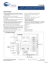
2.0 Functional Overview
The CY7C65113C device is a one-time programmable 8-bit microcontroller with a built-in 12-Mbps USB hub that supports up to
four downstream ports. The microcontroller instruction set has been optimized specifically for USB operations, although the
microcontrollers can be used for a variety of non-USB embedded applications.
GPIO
The CY7C65113C has 11 GPIO pins (P0[7:0], P1[2:0]), both rated at 7 mA per pin (typical) sink current. Multiple GPIO pins can
be connected together to drive a single output for more drive current capacity.
Clock
The microcontroller uses an external 6-MHz crystal and an internal oscillator to provide a reference to an internal phase-locked
loop (PLL)-based clock generator. This technology allows the customer application to use an inexpensive 6-MHz fundamental
crystal that reduces the clock-related noise emissions (EMI). A PLL clock generator provides the 6-, 12-, and 48-MHz clock signals
for distribution within the microcontroller.
Memory
The CY7C65113C is offered with 8 KB of PROM.
Power-on Reset, Watchdog, and Free-running Timer
These parts include power-on reset logic, a Watchdog timer, and a 12-bit free-running timer. The POR logic detects when power
is applied to the device, resets the logic to a known state, and begins executing instructions at PROM address 0x0000. The
Watchdog timer is used to ensure the microcontroller recovers after a period of inactivity. The firmware may become inactive for
a variety of reasons, including errors in the code or a hardware failure such as waiting for an interrupt that never occurs.
I
2
C
The microcontroller can communicate with external electronics through the GPIO pins. An I
2
C-compatible interface accommo-
dates a 100-kHz serial link with an external device.
Timer
The free-running 12-bit timer clocked at 1 MHz provides two interrupt sources, 128-µs and 1.024-ms. The timer can be used to
measure the duration of an event under firmware control by reading the timer at the start of the event and after the event is
complete. The difference between the two readings indicates the duration of the event in microseconds. The upper four bits of
the timer are latched into an internal register when the firmware reads the lower eight bits. A read from the upper four bits actually
reads data from the internal register, instead of the timer. This feature eliminates the need for firmware to try to compensate if the
upper four bits increment immediately after the lower eight bits are read.
Interrupts
The microcontroller supports ten maskable interrupts in the vectored interrupt controller. Interrupt sources include the USB Bus
Reset interrupt, the 128-µs (bit 6) and 1.024-ms (bit 9) outputs from the free-running timer, five USB endpoints, the USB hub, the
GPIO ports, and the I
2
C-compatible master mode interface. The timer bits cause an interrupt (if enabled) when the bit toggles
from LOW ‘0’ to HIGH ‘1’. The USB endpoints interrupt after the USB host has written data to the endpoint FIFO or after the USB
controller sends a packet to the USB host. The GPIO ports also have a level of masking to select which GPIO inputs can cause
a GPIO interrupt. Input transition polarity can be programmed for each GPIO port as part of the port configuration. The interrupt
polarity can be rising edge (‘0’ to ‘1’) or falling edge (‘1’ to ‘0’).
USB
The CY7C65113C includes an integrated USB Serial Interface Engine (SIE) that supports the integrated peripherals and the hub
controller function. The hardware supports up to two USB device addresses with one device address for the hub (two endpoints)
and a device address for a compound device (three endpoints). The SIE allows the USB host to communicate with the hub and
functions integrated into the microcontroller. The CY7C65113C part includes a 1:4 hub repeater with one upstream port and four
downstream ports. The USB Hub allows power management control of the downstream ports by using GPIO pins assigned by
the user firmware. The user has the option of ganging the downstream ports together with a single pair of power management
pins, or providing power management for each port with four pairs of power management pins.
[+] Feedback

CY7C65113C
Document #: 38-08002 Rev. *D Page 7 of 49
Logic Block Diagram
Interrupt
Controller
PROM
12-bit
Timer
Reset
Watchdog
Timer
Repeater
Power-on
SCLK
I
2
C comp.
USB
Transceiver
USB
Transceiver
USB
Transceiver
GPIO
PORT 1
GPIO
PORT 0
P0[0]
P0[7]
P1[0]
P1[2]
SDATA
D+[3]
D–[3]
D+[2]
D–[2]
8-bit Bus
6-MHz crystal
RAM
USB
SIE
USB
Transceiver
D+[4]
D–[4]
USB
Transceiver
D+[0]
D–[0]
D+[1]
D–[1]
Upstream
USB Port
256 byte
8 KB
Clock
6 MHz
12-MHz
8-bit
CPU
Power management under firmware
control using GPIO pins
Interface
PLL
12 MHz
48 MHz
Divider
Downstream USB Ports
*I
2
C-compatible interface enabled by firmware through
P1[1:0]
[+] Feedback

CY7C65113C
Document #: 38-08002 Rev. *D Page 8 of 49
4.0 Product Summary Tables
4.1 Pin Assignments
3.0 Pin Configurations
Table 4-1. Pin Assignments
Name I/O 28-pin Description
D+[0], D–[0] I/O 5, 6 Upstream port, USB differential data.
D+[1], D–[1] I/O 7, 8 Downstream Port 1, USB differential data.
D+[2], D–[2] I/O 9, 10 Downstream Port 2, USB differential data.
D+[3], D–[3] I/O 23, 24 Downstream Port 3, USB differential data.
D+[4], D–[4] I/O 21, 22 Downstream Port 4, USB differential data.
P0 I/O P1[7:0]
11, 15, 12, 16, 13, 17, 14, 18
GPIO Port 0 capable of sinking 7 mA (typical).
P1 I/O P1[2:0]
25, 27, 26
GPIO Port 1 capable of sinking 7 mA (typical).
XTAL
IN
IN 2 6-MHz crystal or external clock input.
XTAL
OUT
OUT 1 6-MHz crystal out.
V
PP
19 Programming voltage supply, tie to ground during normal operation.
V
CC
28 Voltage supply.
GND 4, 20 Ground.
V
REF
IN 3 External 3.3V supply voltage for the downstream differential data output
buffers and the D+ pull-up.
1
2
3
4
5
6
7
9
11
12
13
14
XTALIN
10
8
15
17
16
19
18
21
20
23
22
25
24
26
28
27
V
CC
P1[1]
P1[0]
P1[2]
D–[3]
D+[3]
D–[4]
D+[4]
V
REF
GND
D+[0]
D–[0]
D+[1]
D–[1]
D+[2]
D–[2]
P0[7]
P0[5]
P0[3]
P0[1]
XTALOUT
GND
V
PP
P0[0]
P0[2]
P0[4]
P0[6]
CY7C65113C
28-pin SOIC
Top View
[+] Feedback

CY7C65113C
Document #: 38-08002 Rev. *D Page 9 of 49
4.2 I/O Register Summary
I/O registers are accessed via the I/O Read (IORD) and I/O Write (IOWR, IOWX) instructions. IORD reads data from the selected
port into the accumulator. IOWR performs the reverse; it writes data from the accumulator to the selected port. Indexed I/O Write
(IOWX) adds the contents of X to the address in the instruction to form the port address and writes data from the accumulator to
the specified port. Specifying address 0 (e.g., IOWX 0h) means the I/O register is selected solely by the contents of X.
All undefined registers are reserved. Do not write to reserved registers as this may cause an undefined operation or increased
current consumption during operation. When writing to registers with reserved bits, the reserved bits must be written with ‘0.’
Table 4-2. I/O Register Summary
Register Name I/O Address Read/Write Function Page
Port 0 Data 0x00 R/W GPIO Port 0 Data 17
Port 1 Data 0x01 R/W GPIO Port 1 Data 17
Port 0 Interrupt Enable 0x04 W Interrupt Enable for Pins in Port 0 19
Port 1 Interrupt Enable 0x05 W Interrupt Enable for Pins in Port 1 19
GPIO Configuration 0x08 R/W GPIO Port Configurations 18
I
2
C Configuration 0x09 R/W I
2
C Position Configuration 20
USB Device Address A 0x10 R/W USB Device Address A 34
EP A0 Counter Register 0x11 R/W USB Address A, Endpoint 0 Counter 36
EP A0 Mode Register 0x12 R/W USB Address A, Endpoint 0 Configuration 35
EP A1 Counter Register 0x13 R/W USB Address A, Endpoint 1 Counter 36
EP A1 Mode Register 0x14 R/W USB Address A, Endpoint 1 Configuration 36
EP A2 Counter Register 0x15 R/W USB Address A, Endpoint 2 Counter 36
EP A2 Mode Register 0x16 R/W USB Address A, Endpoint 2 Configuration 36
USB Status & Control 0x1F R/W USB Upstream Port Traffic Status and Control 33
Global Interrupt Enable 0x20 R/W Global Interrupt Enable 24
Endpoint Interrupt Enable 0x21 R/W USB Endpoint Interrupt Enables 24
Interrupt Vector 0x23 R Pending Interrupt Vector Read/Clear 26
Timer (LSB) 0x24 R Lower Eight Bits of Free-running Timer (1 MHz) 20
Timer (MSB) 0x25 R Upper Four Bits of Free-running Timer 20
WDR Clear 0x26 W Watchdog Reset Clear 16
I
2
C Control & Status 0x28 R/W I
2
C Status and Control 21
I
2
C Data 0x29 R/W I
2
C Data 21
Reserved 0x30 Reserved
Reserved 0x31 Reserved
Reserved 0x32 Reserved
Reserved 0x38-0x3F Reserved
USB Device Address B 0x40 R/W USB Device Address B (not used in 5-endpoint mode) 34
EP B0 Counter Register 0x41 R/W USB Address B, Endpoint 0 Counter 36
EP B0 Mode Register 0x42 R/W USB Address B, Endpoint 0 Configuration, or
USB Address A, Endpoint 3 in 5-endpoint mode
35
EP B1 Counter Register 0x43 R/W USB Address B, Endpoint 1 Counter 36
EP B1 Mode Register 0x44 R/W USB Address B, Endpoint 1 Configuration, or
USB Address A, Endpoint 4 in 5-endpoint mode
36
Hub Port Connect Status 0x48 R/W Hub Downstream Port Connect Status 29
Hub Port Enable 0x49 R/W Hub Downstream Ports Enable 30
Hub Port Speed 0x4A R/W Hub Downstream Ports Speed 30
[+] Feedback

CY7C65113C
Document #: 38-08002 Rev. *D Page 10 of 49
4.3 Instruction Set Summary
Refer to the CYASM Assembler User’s Guide for more details. Note that conditional jump instructions (i.e., JC, JNC, JZ, JNZ)
take five cycles if jump is taken, four cycles if no jump.
Hub Port Control (Ports [4:1]) 0x4B R/W Hub Downstream Ports Control (Ports [4:1]) 31
Hub Port Suspend 0x4D R/W Hub Downstream Port Suspend Control 32
Hub Port Resume Status 0x4E R Hub Downstream Ports Resume Status 33
Hub Ports SE0 Status 0x4F R Hub Downstream Ports SE0 Status 31
Hub Ports Data 0x50 R Hub Downstream Ports Differential Data 32
Hub Downstream Force Low 0x51 R/W Hub Downstream Ports Force LOW (Ports [1:4]) 31
Processor Status & Control 0xFF R/W Microprocessor Status and Control Register 23
Table 4-3. Instruction Set Summary
MNEMONIC operand opcode cycles MNEMONIC operand opcode cycles
HALT 00 7 NOP 20 4
ADD A,expr data 01 4 INC A acc 21 4
ADD A,[expr] direct 02 6 INC X x 22 4
ADD A,[X+expr] index 03 7 INC [expr] direct 23 7
ADC A,expr data 04 4 INC [X+expr] index 24 8
ADC A,[expr] direct 05 6 DEC A acc 25 4
ADC A,[X+expr] index 06 7 DEC X x 26 4
SUB A,expr data 07 4 DEC [expr] direct 27 7
SUB A,[expr] direct 08 6 DEC [X+expr] index 28 8
SUB A,[X+expr] index 09 7 IORD expr address 29 5
SBB A,expr data 0A 4 IOWR expr address 2A 5
SBB A,[expr] direct 0B 6 POP A 2B 4
SBB A,[X+expr] index 0C 7 POP X 2C 4
OR A,expr data 0D 4 PUSH A 2D 5
OR A,[expr] direct 0E 6 PUSH X 2E 5
OR A,[X+expr] index 0F 7 SWAP A,X 2F 5
AND A,expr data 10 4 SWAP A,DSP 30 5
AND A,[expr] direct 11 6 MOV [expr],A direct 31 5
AND A,[X+expr] index 12 7 MOV [X+expr],A index 32 6
XOR A,expr data 13 4 OR [expr],A direct 33 7
XOR A,[expr] direct 14 6 OR [X+expr],A index 34 8
XOR A,[X+expr] index 15 7 AND [expr],A direct 35 7
CMP A,expr data 16 5 AND [X+expr],A index 36 8
CMP A,[expr] direct 17 7 XOR [expr],A direct 37 7
CMP A,[X+expr] index 18 8 XOR [X+expr],A index 38 8
MOV A,expr data 19 4 IOWX [X+expr] index 39 6
MOV A,[expr] direct 1A 5 CPL 3A 4
MOV A,[X+expr] index 1B 6 ASL 3B 4
MOV X,expr data 1C 4 ASR 3C 4
MOV X,[expr] direct 1D 5 RLC 3D 4
reserved 1E RRC 3E 4
Table 4-2. I/O Register Summary (continued)
Register Name I/O Address Read/Write Function Page
[+] Feedback

CY7C65113C
Document #: 38-08002 Rev. *D Page 11 of 49
5.0 Programming Model
5.1 14-bit Program Counter
The 14-bit Program Counter (PC) allows access to up to 8 KB of PROM available with the CY7C65113C architecture. The top
32 bytes of the ROM in the 8K part are reserved for testing purposes. The program counter is cleared during reset, such that the
first instruction executed after a reset is at address 0x0000h. Typically, this is a jump instruction to a reset handler that initializes
the application (see Interrupt Vectors on page 25).
The lower eight bits of the program counter are incremented as instructions are loaded and executed. The upper six bits of the
program counter are incremented by executing an XPAGE instruction. As a result, the last instruction executed within a 256-byte
“page” of sequential code should be an XPAGE instruction. The assembler directive “XPAGEON” causes the assembler to insert
XPAGE instructions automatically. Because instructions can be either one or two bytes long, the assembler may occasionally
need to insert a NOP followed by an XPAGE to execute correctly.
The address of the next instruction to be executed, the carry flag, and the zero flag are saved as two bytes on the program stack
during an interrupt acknowledge or a CALL instruction. The program counter, carry flag, and zero flag are restored from the
program stack during a RETI instruction. Only the program counter is restored during a RET instruction.
The program counter cannot be accessed directly by the firmware. The program stack can be examined by reading SRAM from
location 0x00 and up.
XPAGE 1F 4 RET 3F 8
MOV A,X 40 4 DI 70 4
MOV X,A 41 4 EI 72 4
MOV PSP,A 60 4 RETI 73 8
CALL addr 50-5F 10 JC addr C0-CF 5 (or 4)
JMP addr 80-8F 5 JNC addr D0-DF 5 (or 4)
CALL addr 90-9F 10 JACC addr E0-EF 7
JZ addr A0-AF 5 (or 4) INDEX addr F0-FF 14
JNZ addr B0-BF 5 (or 4)
Table 4-3. Instruction Set Summary (continued)
MNEMONIC operand opcode cycles MNEMONIC operand opcode cycles
[+] Feedback

CY7C65113C
Document #: 38-08002 Rev. *D Page 12 of 49
5.1.1 Program Memory Organization
Note that
the upper 32 bytes of the 8K PROM are reserved. Therefore, user’s program must not overwrite this space.
after reset Address
14-bit PC 0x0000 Program execution begins here after a reset
0x0002 USB Bus Reset interrupt vector
0x0004 128-µs timer interrupt vector
0x0006 1.024-ms timer interrupt vector
0x0008 USB address A endpoint 0 interrupt vector
0x000A USB address A endpoint 1 interrupt vector
0x000C USB address A endpoint 2 interrupt vector
0x000E USB address B endpoint 0 interrupt vector
0x0010 USB address B endpoint 1 interrupt vector
0x0012 Hub interrupt vector
0x0014 Reserved
0x0016 GPIO interrupt vector
0x0018
I
2
C interrupt vector
0x001A Program Memory begins here
0x1FDF (8 KB -32) PROM ends here (CY7C65113C)
Figure 5-1. Program Memory Space with Interrupt Vector Table
[+] Feedback

CY7C65113C
Document #: 38-08002 Rev. *D Page 13 of 49
5.2 8-bit Accumulator (A)
The accumulator is the general-purpose register for the microcontroller.
5.3 8-bit Temporary Register (X)
The “X” register is available to the firmware for temporary storage of intermediate results. The microcontroller can perform indexed
operations based on the value in X. Refer to Section 5.6.3 for additional information.
5.4 8-bit Program Stack Pointer (PSP)
During a reset, the Program Stack Pointer (PSP) is set to 0x00 and “grows” upward from this address. The PSP may be set by
firmware, using the MOV PSP,A instruction. The PSP supports interrupt service under hardware control and CALL, RET, and
RETI instructions under firmware control. The PSP is not readable by the firmware.
During an interrupt acknowledge, interrupts are disabled and the 14-bit program counter, carry flag, and zero flag are written as
two bytes of data memory. The first byte is stored in the memory addressed by the PSP, then the PSP is incremented. The second
byte is stored in memory addressed by the PSP, and the PSP is incremented again. The overall effect is to store the program
counter and flags on the program “stack” and increment the PSP by two.
The Return From Interrupt (RETI) instruction decrements the PSP, then restores the second byte from memory addressed by the
PSP. The PSP is decremented again and the first byte is restored from memory addressed by the PSP. After the program counter
and flags have been restored from stack, the interrupts are enabled. The overall effect is to restore the program counter and flags
from the program stack, decrement the PSP by two, and re-enable interrupts.
The Call Subroutine (CALL) instruction stores the program counter and flags on the program stack and increments the PSP by
two.
The Return From Subroutine (RET) instruction restores the program counter but not the flags from the program stack and
decrements the PSP by two.
5.4.1 Data Memory Organization
The CY7C65113C microcontrollers provide 256 bytes of data RAM. Normally, the SRAM is partitioned into four areas: program
stack, user variables, data stack, and USB endpoint FIFOs. The following is one example of where the program stack, data stack,
and user variables areas could be located.
Notes:
1. Refer to Section 5.5 for a description of DSP.
2. Endpoint sizes are fixed by the Endpoint Size Bit (I/O register 0x1F, Bit 7). See Table 17-1.
After reset Address
8-bit DSP 8-bit PSP 0x00 Program Stack Growth
(Move DSP
[1]
)
8-bit DSP
user selected Data Stack Growth
User variables
USB FIFO space for up to two Addresses and five endpoints
[2]
0xFF
[+] Feedback

CY7C65113C
Document #: 38-08002 Rev. *D Page 14 of 49
5.5 8-bit Data Stack Pointer (DSP)
The Data Stack Pointer (DSP) supports PUSH and POP instructions that use the data stack for temporary storage. A PUSH
instruction pre-decrements the DSP, then writes data to the memory location addressed by the DSP. A POP instruction reads
data from the memory location addressed by the DSP, then post-increments the DSP.
During a reset, the DSP is reset to 0x00. A PUSH instruction when DSP equals 0x00 writes data at the top of the data RAM
(address 0xFF). This writes data to the memory area reserved for USB endpoint FIFOs. Therefore, the DSP should be indexed
at an appropriate memory location that does not compromise the Program Stack, user-defined memory (variables), or the USB
endpoint FIFOs.
For USB applications, the firmware should set the DSP to an appropriate location to avoid a memory conflict with RAM dedicated
to USB FIFOs. The memory requirements for the USB endpoints are described in Section 17.2. Example assembly instructions
to do this with two device addresses (FIFOs begin at 0xD8) are shown below:
MOV A,20h ; Move 20 hex into Accumulator (must be D8h or less)
SWAP A,DSP ; swap accumulator value into DSP register.
5.6 Address Modes
The CY7C65113 microcontrollers support three addressing modes for instructions that require data operands: data, direct, and
indexed.
5.6.1 Data (Immediate)
“Data” address mode refers to a data operand that is actually a constant encoded in the instruction. As an example, consider the
instruction that loads A with the constant 0xD8:
• MOV A, 0D8h.
This instruction requires two bytes of code where the first byte identifies the “MOV A” instruction with a data operand as the
second byte. The second byte of the instruction is the constant “0xD8.” A constant may be referred to by name if a prior “EQU”
statement assigns the constant value to the name. For example, the following code is equivalent to the example shown above:
• DSPINIT: EQU 0D8h
• MOV A, DSPINIT.
5.6.2 Direct
“Direct” address mode is used when the data operand is a variable stored in SRAM. In that case, the one byte address of the
variable is encoded in the instruction. As an example, consider an instruction that loads A with the contents of memory address
location 0x10:
• MOV A, [10h].
Normally, variable names are assigned to variable addresses using “EQU” statements to improve the readability of the assembler
source code. As an example, the following code is equivalent to the example shown above:
• buttons: EQU 10h
• MOV A, [buttons].
5.6.3 Indexed
“Indexed” address mode allows the firmware to manipulate arrays of data stored in SRAM. The address of the data operand is
the sum of a constant encoded in the instruction and the contents of the “X” register. Normally, the constant is the “base” address
of an array of data and the X register contains an index that indicates which element of the array is actually addressed:
•array: EQU 10h
•MOV X, 3
• MOV A, [X+array].
This would have the effect of loading A with the fourth element of the SRAM “array” that begins at address 0x10. The fourth
element would be at address 0x13.
[+] Feedback

CY7C65113C
Document #: 38-08002 Rev. *D Page 15 of 49
6.0 Clocking
The XTALIN and XTALOUT are the clock pins to the microcontroller. The user can connect an external oscillator or a crystal to
these pins. When using an external crystal, keep PCB traces between the chip leads and crystal as short as possible (less than
2 cm). A 6-MHz fundamental frequency parallel resonant crystal can be connected to these pins to provide a reference frequency
for the internal PLL. The two internal 30-pF load caps appear in series to the external crystal and would be equivalent to a 15-pF
load. Therefore, the crystal must have a required load capacitance of about 15–18 pF. A ceramic resonator does not allow the
microcontroller to meet the timing specifications of full speed USB and therefore a ceramic resonator is not recommended with
these parts.
An external 6-MHz clock can be applied to the XTALIN pin if the XTALOUT pin is left open. Grounding the XTALOUT pin when
driving XTALIN with an oscillator does not work because the internal clock is effectively shorted to ground.
7.0 Reset
The CY7C65113C supports two resets: POR and WDR. Each of these resets causes:
• all registers to be restored to their default states
• the USB device addresses to be set to 0
• all interrupts to be disabled
• the PSP and DSP to be set to memory address 0x00.
The occurrence of a reset is recorded in the Processor Status and Control Register, as described in Section. Bits 4 and 6 are
used to record the occurrence of POR and WDR respectively. Firmware can interrogate these bits to determine the cause of a
reset.
Program execution starts at ROM address 0x0000 after a reset. Although this looks like interrupt vector 0, there is an important
difference. Reset processing does NOT push the program counter, carry flag, and zero flag onto program stack. The firmware
reset handler should configure the hardware before the “main” loop of code. Attempting to execute a RET or RETI in the firmware
reset handler causes unpredictable execution results.
7.1 Power-on Reset
When V
CC
is first applied to the chip, the POR signal is asserted and the CY7C65113C enters a “semi-suspend” state. During
the semi-suspend state, which is different from the suspend state defined in the USB specification, the oscillator and all other
blocks of the part are functional, except for the CPU. This semi-suspend time ensures that both a valid V
CC
level is reached and
that the internal PLL has time to stabilize before full operation begins. When the V
CC
has risen above approximately 2.5V, and
the oscillator is stable, the POR is deasserted and the on-chip timer starts counting. The first 1 ms of suspend time is not
interruptible, and the semi-suspend state continues for an additional 95 ms unless the count is bypassed by a USB Bus Reset
on the upstream port. The 95 ms provides time for V
CC
to stabilize at a valid operating voltage before the chip executes code.
If a USB Bus Reset occurs on the upstream port during the 95 ms semi-suspend time, the semi-suspend state is aborted and
program execution begins immediately from address 0x0000. In this case, the Bus Reset interrupt is pending but not serviced
until firmware sets the USB Bus Reset Interrupt Enable bit (Bit 0, Figure 14-1) and enables interrupts with the EI command.
The POR signal is asserted whenever V
CC
drops below approximately 2.5V, and remains asserted until V
CC
rises above this level
again. Behavior is the same as described above.
XTALOUT
XTALIN
To Internal PLL
30 pF
30 pF
(pin 1)
(pin 2)
Figure 6-1. Clock Oscillator On-Chip Circuit
[+] Feedback

CY7C65113C
Document #: 38-08002 Rev. *D Page 16 of 49
7.2 Watchdog Reset
The WDR occurs when the internal Watchdog Timer rolls over. Writing any value to the write-only Watchdog Reset Clear Register
(Figure 7-1) clears the timer. The timer rolls over and WDR occurs if it is not cleared within t
WATCH
of the last clear (see Section
23.0 for the value of t
WATCH
). Bit 6 of the Processor Status and Control Register (Figure 13-1) is set to record this event (the
register contents are set to 010X0001 by the WDR). A Watchdog Timer Reset lasts for 2 ms, after which the microcontroller begins
execution at ROM address 0x0000.
The USB transmitter is disabled by a Watchdog Reset because the USB Device Address Registers are cleared (see Section
17.1). Otherwise, the USB Controller would respond to all address 0 transactions.
It is possible for the WDR bit of the Processor Status and Control Register (Figure 13-1) to be set following a POR event. If a
firmware interrogates the Processor Status and Control Register for a set condition on the WDR bit, the WDR bit should be ignored
if the POR bit is set (Bit 3 of the Processor Status and Control Register).
8.0 Suspend Mode
The CY7C65113C can be placed into a low-power state by setting the Suspend bit of the Processor Status and Control register.
All logic blocks in the device are turned off except the GPIO interrupt logic and the USB receiver. The clock oscillator and PLL,
as well as the free-running and Watchdog timers, are shut down. Only the occurrence of an enabled GPIO interrupt or non-idle
bus activity at a USB upstream or downstream port wakes the part out of suspend. The Run bit in the Processor Status and
Control Register must be set to resume a part out of suspend.
The clock oscillator restarts immediately after exiting suspend mode. The microcontroller returns to a fully functional state 1 ms
after the oscillator is stable. The microcontroller executes the instruction following the I/O write that placed the device into suspend
mode before servicing any interrupt requests.
The GPIO interrupt allows the controller to wake-up periodically and poll system components while maintaining a very low average
power consumption. To achieve the lowest possible current during suspend mode, all I/O should be held at V
CC
or Gnd. Note:
This also applies to internal port pins that may not be bonded in a particular package.
Typical code for entering suspend is shown below:
... ; All GPIO set to low-power state (no floating pins)
... ; Enable GPIO interrupts if desired for wake-up
mov a, 09h ; Set suspend and run bits
iowr FFh ; Write to Status and Control Register – Enter suspend, wait for USB activity (or GPIO Interrupt)
nop ; This executes before any ISR
... ; Remaining code for exiting suspend routine.
Last write to
Watchdog Timer
Register
No write to WDT
register, so WDR
goes HIGH
Execution begins at
Reset Vector 0x0000
t
WATCH
2 ms
Figure 7-1. Watchdog Reset (Address 0x26)
[+] Feedback

CY7C65113C
Document #: 38-08002 Rev. *D Page 17 of 49
9.0 General-purpose I/O Ports
There are 11 GPIO pins (P0[7:0] and P1[2:0]) for the hardware interface. Each port can be configured as inputs with internal
pull-ups, open drain outputs, or traditional CMOS outputs. The data for each GPIO port is accessible through the data registers.
Port data registers are shown in Figure 9-2 through Figure 9-3, and are set to 1 on reset.
.
Special care should be taken with any unused GPIO data bits. An unused GPIO data bit, either a pin on the chip or a port bit that
is not bonded on a particular package, must not be left floating when the device enters the suspend state. If a GPIO data bit is
left floating, the leakage current caused by the floating bit may violate the suspend current limitation specified by the USB
Specifications. If a ‘1’ is written to the unused data bit and the port is configured with open drain outputs, the unused data bit
remains in an indeterminate state. Therefore, if an unused port bit is programmed in open-drain mode, it must be written with a ‘0.’
A read from a GPIO port always returns the present state of the voltage at the pin, independent of the settings in the Port Data
Registers. During reset, all of the GPIO pins are set to a high-impedance input state. Writing a ‘0’ to a GPIO pin drives the pin
LOW. In this state, a ‘0’ is always read on that GPIO pin unless an external source overdrives the internal pull-down device.
Figure 9-1. Block Diagram of a GPIO Pin
Port 0 Data Address 0x00
Bit # 76543210
Bit Name P0.7 P0.6 P0.5 P0.4 P0.3 P0.2 P0.1 P0.0
Read/Write R/W R/W R/W R/W R/W R/W R/W R/W
Reset 11111111
Figure 9-2. Port 0 Data
Port 1 Data Address 0x01
Bit # -----210
Bit Name - - - - - P1.2 P1.1 P1.0
Read/Write-----R/WR/WR/W
Reset -----111
Figure 9-3. Port1 Data
GPIO
V
CC
14 kΩ
GPIO
CFG
mode
2-bits
Data
Out
Latch
Internal
Data Bus
Port Read
Port Write
Interrupt
Enable
Control
Control
Interrupt
Controller
Q1
Q3*
Q2
*Port 0,1: Low I
sink
Data
Interrupt
Latch
OE
Reg_Bit
STRB
Data
In
Latch
(Latch is Transparent)
PIN
[+] Feedback

CY7C65113C
Document #: 38-08002 Rev. *D Page 18 of 49
9.1 GPIO Configuration Port
Every GPIO port can be programmed as inputs with internal pull-ups, outputs LOW or HIGH, or Hi-Z (floating, the pin is not driven
internally). In addition, the interrupt polarity for each port can be programmed. The Port Configuration bits (Figure 9-4) and the
Interrupt Enable bit (Figure 9-5 through Figure 9-6) determine the interrupt polarity of the port pins
.
As shown in Table 9-1 below, a positive polarity on an input pin represents a rising edge interrupt (LOW to HIGH), and a negative
polarity on an input pin represents a falling edge interrupt (HIGH to LOW).
The GPIO interrupt is generated when all of the following conditions are met: the Interrupt Enable bit of the associated Port
Interrupt Enable Register is enabled, the GPIO Interrupt Enable bit of the Global Interrupt Enable Register (Figure 14-1) is
enabled, the Interrupt Enable Sense (bit 2, Figure 13-1) is set, and the GPIO pin of the port sees an event matching the interrupt
polarity.
The driving state of each GPIO pin is determined by the value written to the pin’s Data Register (Figure 9-2 through Figure 9-3)
and by its associated Port Configuration bits as shown in the GPIO Configuration Register (Figure 9-4). These ports are
configured on a per-port basis, so all pins in a given port are configured together. The possible port configurations are detailed
in Tab le 9-1. As shown in this table below, when a GPIO port is configured with CMOS outputs, interrupts from that port are
disabled.
During reset, all of the bits in the GPIO Configuration Register are written with ‘0’ to select Hi-Z mode for all GPIO ports as the
default configuration.
GPIO Configuration Address 0x08
Bit # 76543210
Bit Name Reserved Reserved Reserved Reserved Port 1
Config Bit 1
Port 1
Config Bit 0
Port 0
Config Bit 1
Port 0
Config Bit 0
Read/Write - - - - R/W R/W R/W R/W
Reset ----0000
Figure 9-4. GPIO Configuration Register
[+] Feedback

CY7C65113C
Document #: 38-08002 Rev. *D Page 19 of 49
Q1, Q2, and Q3 discussed below are the transistors referenced in Figure 9-1. The available GPIO drive strength are:
• Output LOW Mode: The pin’s Data Register is set to ‘0.’
Writing ‘0’ to the pin’s Data Register puts the pin in output LOW mode, regardless of the contents of the Port Configuration
Bits[1:0]. In this mode, Q1 and Q2 are OFF. Q3 is ON. The GPIO pin is driven LOW through Q3.
• Output HIGH Mode: The pin’s Data Register is set to 1 and the Port Configuration Bits[1:0] is set to ‘10.’
In this mode, Q1 and Q3 are OFF. Q2 is ON. The GPIO is pulled up through Q2. The GPIO pin is capable of sourcing... of
current.
• Resistive Mode: The pin’s Data Register is set to 1 and the Port Configuration Bits[1:0] is set to ‘11.’
Q2 and Q3 are OFF. Q1 is ON. The GPIO pin is pulled up with an internal 14kΩ resistor. In resistive mode, the pin may serve
as an input. Reading the pin’s Data Register returns a logic HIGH if the pin is not driven LOW by an external source.
• Hi-Z Mode: The pin’s Data Register is set to1 and Port Configuration Bits[1:0] is set either ‘00’ or ‘01.’
Q1, Q2, and Q3 are all OFF. The GPIO pin is not driven internally. In this mode, the pin may serve as an input. Reading the
Port Data Register returns the actual logic value on the port pins.
9.2 GPIO Interrupt Enable Ports
Each GPIO pin can be individually enabled or disabled as an interrupt source. The Port 0–1 Interrupt Enable Registers provide
this feature with an Interrupt Enable bit for each GPIO pin.
During a reset, GPIO interrupts are disabled by clearing all of the GPIO Interrupt Enable bits. Writing a ‘1’ to a GPIO Interrupt
Enable bit enables GPIO interrupts from the corresponding input pin. All GPIO pins share a common interrupt, as discussed in
Section 14.7.
.
10.0 12-bit Free-Running Timer
The 12-bit timer operates with a 1-µs tick, provides two interrupts (128 µs and 1.024 ms) and allows the firmware to directly time
events that are up to 4 ms in duration. The lower eight bits of the timer can be read directly by the firmware. Reading the lower
eight bits latches the upper four bits into a temporary register. When the firmware reads the upper four bits of the timer, it is actually
reading the count stored in the temporary register. The effect of this is to ensure a stable 12-bit timer value can be read, even
when the two reads are separated in time.
Table 9-1. GPIO Port Output Control Truth Table and Interrupt Polarity
Port Config Bit 1 Port Config Bit 0 Data Register Output Drive Strength Interrupt Enable Bit Interrupt Polarity
1 1 0 Output LOW 0 Disabled
1 Resistive 1 – (Falling Edge)
1 0 0 Output LOW 0 Disabled
1 Output HIGH 1 Disabled
0 1 0 Output LOW 0 Disabled
1 Hi-Z 1 – (Falling Edge)
0 0 0 Output LOW 0 Disabled
1 Hi-Z 1 + (Rising Edge)
Port 0 Interrupt Enable Address 0x04
Bit # 76543210
Bit Name P0.7 Intr
Enable
P0.6 Intr
Enable
P0.5 Intr
Enable
P0.4 Intr
Enable
P0.3 Intr
Enable
P0.2 Intr
Enable
P0.1 Intr
Enable
P0.0 Intr
Enable
Read/WriteWWWWWWWW
Reset 00000000
Figure 9-5. Port 0 Interrupt Enable
Port 1 Interrupt Enable Address 0x05
Bit # 76543210
Bit Name Reserved Reserved Reserved Reserved Reserved P0.2 Intr
Enable
P1.1 Intr
Enable
P1.0 Intr
Enable
Read/Write-----WWW
Reset -----000
Figure 9-6. Port 1 Interrupt Enable
[+] Feedback

CY7C65113C
Document #: 38-08002 Rev. *D Page 20 of 49
Bit [7:0]: Timer lower eight bits.
Bit [3:0]: Timer higher nibble
Bit [7:4]: Reserved.
11.0 I
2
C Configuration Register
Internal hardware supports communication with external devices through an I
2
C-compatible interface. I
2
C-compatible function is
discussed in detail in Section 12.0.
[3]
The I
2
C Position bit (Bit 7, Figure 11-1) and I
2
C Port Width bit (Bit 1, Figure 11-1) select the
locations of the SCL (clock) and SDA (data) pins on Port 1 as shown in Table 11-1. These bits are cleared on reset. When the
GPIO is configured for I
2
C function, the internal pull ups on the pins are disabled. Addition of an external weak pull-up resistors
on SCL and SDA is recommended.
.
Timer LSB Address 0x24
Bit # 76543210
Bit Name Timer Bit 7 TimerBit 6 Timer Bit 5 Timer Bit 4 Timer Bit 3 Timer Bit 2 Timer Bit 1 Timer Bit 0
Read/WriteRRRRRRRR
Reset 00000000
Figure 10-1. Timer LSB Register
Timer MSB Address 0x25
Bit # 76543210
Bit Name Reserved Reserved Reserved Reserved Timer Bit 11 Timer Bit 10 Timer Bit 9 Timer Bit 8
Read/Write – – – – R R R R
Reset 00000000
Figure 10-2. Timer MSB Register
I
2
C Configuration Address 0x09
Bit # 76543210
Bit Name I
2
C Position Reserved Reserved Reserved Reserved Reserved I
2
C Port
Width
Reserved
Read/Write R/W R/W R/W R/W R/W R/W R/W R/W
Reset 00000000
Figure 11-1. I
2
C Configuration Register
Table 11-1. I
2
C Port Configuration
I
2
C Position (Bit7, Figure 11-1)I
2
C Port Width (Bit1, Figure 11-1)I
2
C Position
00I
2
C on P1[1:0], 0:SCL, 1:SDA
10 9 7856 432
1 MHz clock
1.024-ms interrupt
128-
µs interrupt
To Timer Registers
8
1 011
L1 L0L2L3
D3 D2 D1 D0 D7 D6 D5 D4 D3 D2 D1 D0
Figure 10-3. Timer Block Diagram
Note:
3. I
2
C-compatible function must be separately enabled, as described in Section 12.0.
[+] Feedback
/