Page is loading ...

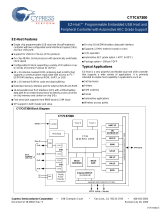
EZ-OTG™ Programmable USB
On-The-Go
CY7C67200
Cypress Semiconductor Corporation • 198 Champion Court • San Jose, CA 95134-1709 • 408-943-2600
Document #: 38-08014 Rev. *G Revised November 14, 2006
EZ-OTG Features
• Single-chip programmable USB dual-role (Host/Peripheral)
controller with two configurable Serial Interface Engines
(SIEs) and two USB ports
• Supports USB OTG protocol
• On-chip 48-MHz 16-bit processor with dynamically
switchable clock speed
• Configurable IO block supports a variety of IO options or up
to 25 bits of General Purpose IO (GPIO)
• 4K × 16 internal mask ROM contains built-in BIOS that
supports a communication-ready state with access to I
2
C™
EEPROM interface, external ROM, UART, or USB
• 8K x 16 internal RAM for code and data buffering
• 16-bit parallel host port interface (HPI) with DMA/Mailbox
data path for an external processor to directly access all
on-chip memory and control on-chip SIEs
• Fast serial port supports from 9600 baud to 2.0M baud
• SPI supports both master and slave
• Supports 12 MHz external crystal or clock
• 2.7V to 3.6V power supply voltage
• Package option: 48-pin FBGA
Typical Applications
EZ-OTG is a very powerful and flexible dual-role USB
controller that supports a wide variety of applications. It is
primarily intended to enable USB OTG capability in applica-
tions such as:
• Cellular phones
• PDAs and pocket PCs
• Video and digital still cameras
• MP3 players
• Mass storage devices
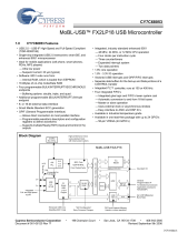
Timer 0 Timer 1
Watchdog
Control
4Kx16
ROM BIOS
8Kx16
RAM
CY16
16-bit RISC CORE
SIE1
USB-A
SIE2
USB-A
OTG
HOST/
Peripheral
USB Ports
D+,D-
D+,D-
UART I/F
HSS I/F
I2C
EEPROM I/F
HPI I/F
SPI I/F
nRESET
CY7C67200
GPIO [24:0]
PLL
X1
X2
GPIO
SHARED INPUT/OUTPUT PINS
Vbus, ID
Mobile
Power
Booster
Block Diagram
CY7C67200
[+] Feedback

CY7C67200
Document #: 38-08014 Rev. *G Page 2 of 78
Introduction
EZ-OTG™ (CY7C67200) is Cypress Semiconductor’s first
USB On-The-Go (OTG) host/peripheral controller. EZ-OTG is
designed to easily interface to most high-performance CPUs
to add USB host functionality. EZ-OTG has its own 16-bit RISC
processor to act as a coprocessor or operate in standalone
mode. EZ-OTG also has a programmable IO interface block
allowing a wide range of interface options.
Processor Core Functional Overview
An overview of the processor core components are presented
in this section.
Processor
EZ-OTG has a general purpose 16-bit embedded RISC
processor that runs at 48 MHz.
Clocking
EZ-OTG requires a 12 MHz source for clocking. Either an
external crystal or TTL-level oscillator may be used. EZ-OTG
has an internal PLL that produces a 48 MHz internal clock from
the 12 MHz source.
Memory
EZ-OTG has a built-in 4K × 16 masked ROM and an 8K × 16
internal RAM. The masked ROM contains the EZ-OTG BIOS.
The internal RAM can be used for program code or data.
Interrupts
EZ-OTG provides 128 interrupt vectors. The first 48 vectors
are hardware interrupts and the following 80 vectors are
software interrupts.
General Timers and Watchdog Timer
EZ-OTG has two built-in programmable timers and a
watchdog timer. All three timers can generate an interrupt to
the EZ-OTG.
Power Management
EZ-OTG has one main power-saving mode, Sleep. Sleep
mode pauses all operations and provides the lowest power
state.
Interface Descriptions
EZ-OTG has a variety of interface options for connectivity, with
several interface options available. See Table 1 to understand
how the interfaces share pins and can coexist. Below are
some general guidelines:
• I2C EEPROM and OTG do not conflict with any interfaces
• HPI is mutually exclusive to HSS, SPI, and UART
Table 1. Interface Options for GPIO Pins
GPIO Pins HPI HSS SPI UART I2C OTG
GPIO31 SCL/SDA
GPIO30 SCL/SDA
GPIO29 OTGID
GPIO24 INT
GPIO23 nRD
GPIO22 nWR
GPIO21 nCS
GPIO20 A1
GPIO19 A0
GPIO15 D15 CTS
GPIO14 D14 RTS
GPIO13 D13 RXD
GPIO12 D12 TXD
GPIO11 D11 MOSI
GPIO10 D10 SCK
GPIO9 D9 nSSI
GPIO8 D8 MISO
GPIO7 D7 TX
GPIO6 D6 RX
GPIO5 D5
GPIO4 D4
GPIO3 D3
GPIO2 D2
GPIO1 D1
GPIO0 D0
[+] Feedback

CY7C67200
Document #: 38-08014 Rev. *G Page 3 of 78
USB Interface
EZ-OTG has two built-in Host/Peripheral SIEs that each have
a single USB transceiver, meeting the USB 2.0 specification
requirements for full and low speed (high speed is not support-
ed). In Host mode, EZ-OTG supports two downstream ports;
each supports control, interrupt, bulk, and isochronous trans-
fers. In Peripheral mode, EZ-OTG supports one peripheral
port with eight endpoints for each of the two SIEs. Endpoint 0
is dedicated as the control endpoint and only supports control
transfers. Endpoints 1 though 7 support Interrupt, bulk (up to
64 bytes per packet), or isochronous transfers (up to 1023
bytes per packet size). EZ-OTG also supports a combination
of Host and Peripheral ports simultaneously, as shown in
Table 2.
USB Features
• USB 2.0 compatible for full and low speed
• Up to two downstream USB host ports
• Up to two upstream USB peripheral ports
• Configurable endpoint buffers (pointer and length), must
reside in internal RAM
• Up to eight available peripheral endpoints (1 control
endpoint)
• Supports Control, Interrupt, Bulk, and Isochronous transfers
• Internal DMA channels for each endpoint
• Internal pull up and pull down resistors
• Internal Series termination resistors on USB data lines
USB Pins
OTG Interface
EZ-OTG has one USB port that is compatible with the USB
On-The-Go supplement to the USB 2.0 specification. The USB
OTG port has various hardware features to support Session
Request Protocol (SRP) and Host Negotiation Protocol (HNP).
OTG is only supported on USB PORT 1A.
OTG Features
• Internal Charge Pump to supply and control VBUS
• VBUS Valid Status (above 4.4V)
• VBUS Status for 2.4V < VBUS < 0.8V
• ID Pin Status
• Switchable 2-Kohm internal discharge resistor on VBUS
• Switchable 500-ohm internal pull-up resistor on VBUS
• Individually switchable internal pull-up and pull-down
resistors on the USB data lines
OTG Pins
General Purpose IO Interface
EZ-OTG has up to 25 GPIO signals available. Several other
optional interfaces use GPIO pins as well and may reduce the
overall number of available GPIOs.
GPIO Description
All Inputs are sampled asynchronously with state changes oc-
curring at a rate of up to two 48 MHz clock cycles. GPIO pins
are latched directly into registers, a single flip-flop.
Unused Pin Descriptions
Unused USB pins must be tri-stated with the D+ line pulled
high through the internal pull-up resistor and the D– line pulled
low through the internal pull-down resistor.
Unused GPIO pins must be configured as outputs and driven
low.
UART Interface
EZ-OTG has a built-in UART interface. The UART interface
supports data rates from 900 to 115.2K baud. It can be used
as a development port or for other interface requirements. The
UART interface is exposed through GPIO pins.
Table 2. USB Port Configuration Options
Port Configurations Port 1A Port 2A
OTG OTG –
OTG + 1 Host OTG Host
OTG + 1 Peripheral OTG Peripheral
1 Host + 1 Peripheral Host Peripheral
1 Host + 1 Peripheral Peripheral Host
2 Hosts Host Host
1 Host Host –
1 Host – Host
2 Peripherals Peripheral Peripheral
1 Peripheral Peripheral –
1 Peripheral – Peripheral
Table 3. USB Interface Pins
Pin Name Pin Number
DM1A F2
DP1A E3
DM2A C2
DP2A D3
Table 4. OTG Interface Pins
Pin Name Pin Number
DM1A F2
DP1A E3
OTGVBUS C1
OTGID F4
CSwitchA D1
CSwitchB D2
[+] Feedback

CY7C67200
Document #: 38-08014 Rev. *G Page 4 of 78
UART Features
• Supports baud rates of 900 to 115.2K
•8-N-1
UART Pins
I
2
C EEPROM Interface
EZ-OTG provides a master-only I2C interface for external se-
rial EEPROMs. The serial EEPROM can be used to store ap-
plication-specific code and data. This I2C interface is only to
be used for loading code out of EEPROM, it is not a general
I2C interface. The I2C EEPROM interface is a BIOS imple-
mentation and is exposed through GPIO pins. Refer to the
BIOS documentation for additional details on this interface.
I
2
C EEPROM Features
• Supports EEPROMs up to 64 KB (512K bit)
• Auto-detection of EEPROM size
I
2
C EEPROM Pins
Serial Peripheral Interface
EZ-OTG provides an SPI interface for added connectivity.
EZ-OTG may be configured as either an SPI master or SPI
slave. The SPI interface can be exposed through GPIO pins
or the External Memory port.
SPI Features
• Master or slave mode operation
• DMA block transfer and PIO byte transfer modes
• Full duplex or half duplex data communication
• 8-byte receive FIFO and 8-byte transmit FIFO
• Selectable master SPI clock rates from 250 kHz to 12 MHz
• Selectable master SPI clock phase and polarity
• Slave SPI signaling synchronization and filtering
• Slave SPI clock rates up to 2 MHz
• Maskable interrupts for block and byte transfer modes
• Individual bit transfer for non-byte aligned serial communi-
cation in PIO mode
• Programmable delay timing for the active/inactive master
SPI clock
• Auto or manual control for master mode slave select signal
• Complete access to internal memory
SPI Pins
The SPI port has a few different pin location options as shown
in Table 7. The pin location is selectable via the GPIO Control
register [0xC006].
High-Speed Serial Interface
EZ-OTG provides an HSS interface. The HSS interface is a
programmable serial connection with baud rate from 9600
baud to 2M baud. The HSS interface supports both byte and
block mode operations as well as hardware and software
handshaking. Complete control of EZ-OTG can be accom-
plished through this interface via an extensible API and com-
munication protocol. The HSS interface can be exposed
through GPIO pins or the External Memory port.
HSS Features
• 8-bit, no parity code
• Programmable baud rate from 9600 baud to 2M baud
• Selectable 1- or 2-stop bit on transmit
• Programmable intercharacter gap timing for Block Transmit
• 8-byte receive FIFO
• Glitch filter on receive
• Block mode transfer directly to/from EZ-OTG internal
memory (DMA transfer)
• Selectable CTS/RTS hardware signal handshake protocol
• Selectable XON/XOFF software handshake protocol
• Programmable Receive interrupt, Block Transfer Done
interrupts
• Complete access to internal memory
HSS Pins
Table 5. UART Interface Pins
Pin Name Pin Number
TX B5
RX B4
Table 6. I
2
C EEPROM Interface Pins
Pin Name Pin Number
SMALL EEPROM
SCK H3
SDA F3
LARGE EEPROM
SCK F3
SDA H3
Table 7. SPI Interface Pins
Pin Name Pin Number
nSSI F6 or C6
SCK D5
MOSI D4
MISO C5
Table 8. HSS Interface Pins
Pin Name Pin Number
CTS F6
RTS E4
RX E5
TX E6
[+] Feedback

CY7C67200
Document #: 38-08014 Rev. *G Page 5 of 78
Host Port Interface (HPI)
EZ-OTG has an HPI interface. The HPI interface provides
DMA access to the EZ-OTG internal memory by an external
host, plus a bidirectional mailbox register for supporting
high-level communication protocols. This port is designed to
be the primary high-speed connection to a host processor.
Complete control of EZ-OTG can be accomplished through
this interface via an extensible API and communication
protocol. Other than the hardware communication protocols, a
host processor has identical control over EZ-Host whether
connecting to the HPI or HSS port. The HPI interface is
exposed through GPIO pins.
Note It should be noted that for up to 3 ms after BIOS starts
executing, GPIO[24:19] and GPIO[15:8] will be driven as
outputs for a test mode. If these pins need to be used as inputs,
a series resistor is required (10 ohm to 48 ohm is recom-
mended). Refer to BIOS documentation for addition details.
See section “Reset Pin” on page 9.
HPI Features
• 16-bit data bus interface
• 16 MB/s throughput
• Auto-increment of address pointer for fast block mode
transfers
• Direct memory access (DMA) to internal memory
• Bidirectional Mailbox register
• Byte Swapping
• Complete access to internal memory
• Complete control of SIEs through HPI
• Dedicated HPI Status register
HPI Pins
The two HPI address pins are used to address one of four
possible HPI port registers as shown in Table 10 below.
Charge Pump Interface
VBUS for the USB On-The-Go (OTG) port can be produced by
EZ-OTG using its built-in charge pump and some external
components. The circuit connections should look similar to
Figure 1 below.
Component details:
• D1 and D2: Schottky diodes with a current rating greater
than 60 mA.
• C1: Ceramic capacitor with a capacitance of 0.1 µF.
• C2: Capacitor value must be no more that 6.5 µF since that
is the maximum capacitance allowed by the USB OTG
specification for a dual-role device. The minimum value of
C2 is 1 µF. There are no restrictions on the type of capacitor
for C2.
If the VBUS charge pump circuit is not to be used,
CSWITCHA, CSWITCHB, and OTGVBUS can be left uncon-
nected.
Table 9. HPI Interface Pins
[1, 2]
Pin Name Pin Number
INT H4
nRD G4
nWR H5
nCS G5
A1 H6
A0 F5
D15 F6
D14 E4
D13 E5
D12 E6
D11 D4
D10 D5
D9 C6
D8 C5
Notes
1. HPI_INT is for the Outgoing Mailbox Interrupt.
2. HPI strobes are negative logic sampled on rising edge.
D7 B5
D6 B4
D5 C4
D4 B3
D3 A3
D2 C3
D1 A2
D0 B2
Table 10.HPI Addressing
HPI A[1:0] A1 A0
HPI Data 0 0
HPI Mailbox 0 1
HPI Address 1 0
HPI Status 1 1
Figure 1. Charge Pump
Table 9. HPI Interface Pins
[1, 2]
(continued)
Pin Name Pin Number
CSWITCHA
CY7C67200
CSWITCHB
OTGVBUS
D1
D2
C1
C2
VBUS
[+] Feedback

CY7C67200
Document #: 38-08014 Rev. *G Page 6 of 78
Charge Pump Features
• Meets OTG Supplement Requirements, see Table 41, “DC
Characteristics: Charge Pump,” on page 66.
Charge Pump Pins
Booster Interface
EZ-OTG has an on-chip power booster circuit for use with
power supplies that range between 2.7V and 3.6V. The
booster circuit boosts the power to 3.3V nominal to supply
power for the entire chip. The booster circuit requires an
external inductor, diode, and capacitor. During power down
mode, the circuit is disabled to save power. Figure 2 shows
how to connect the booster circuit.
Component details:
• L1: Inductor with inductance of 10 µH and a current rating
of at least 250 mA
• D1: Schottky diode with a current rating of at least 250 mA
• C1: Tantalum or ceramic capacitor with a capacitance of at
least 2.2 µF
Figure 3 shows how to connect the power supply when the
booster circuit is not being used.
Booster Pins
Crystal Interface
The recommended crystal circuit to be used with EZ-OTG is
shown in Figure 4. If an oscillator is used instead of a crystal
circuit, connect it to XTALIN and leave XTALOUT uncon-
nected. For further information on the crystal requirements,
see Table 39, “Crystal Requirements,” on page 65.
Table 11.Charge Pump Interface Pins
Pin Name Pin Number
OTGVBUS C1
CSwitchA D1
CSwitchB D2
Figure 2. Power Supply Connection With Booster
BOOSTVcc
VSWITCH
VCC
AVCC
C1
D1
L1
3.3V
2.7V to 3.6V
Power Supply
Figure 3. Power Supply Connection Without Booster
Table 12.Charge Pump Interface Pins
Pin Name Pin Number
BOOSTVcc F1
VSWITCH E2
Figure 4. Crystal Interface
BOOSTVcc
VSWITCH
VCC
AVCC
3.0V to 3.6V
Power Supply
Y1
C1 = 22 pF
C2 = 22 pF
CY7C67200
XTALIN
XTALOUT
12MHz
Parallel Resonant
Fundamental Mode
500uW
20-33pf ±5%
[+] Feedback

CY7C67200
Document #: 38-08014 Rev. *G Page 7 of 78
Crystal Pins
Boot Configuration Interface
EZ-OTG can boot into any one of four modes. The mode it
boots into is determined by the TTL voltage level of
GPIO[31:30] at the time nRESET is deasserted. Table 14
shows the different boot pin combinations possible. After a
reset pin event occurs, the BIOS bootup procedure executes
for up to 3 ms. GPIO[31:30] are sampled by the BIOS during
bootup only. After bootup these pins are available to the appli-
cation as GPIOs.
GPIO[31:30] must be pulled high or low, as needed, using
resistors tied to V
CC
or GND with resistor values between 5K
ohm and 15K ohm. GPIO[31:30] must not be tied directly to
V
CC
or GND. Note that in Standalone mode, the pull ups on
those two pins are used for the serial I2C EEPROM (if imple-
mented). The resistors used for these pull ups must conform
to the serial EEPROM manufacturer's requirements.
If any mode other then standalone is chosen, EZ-OTG will be
in coprocessor mode. The device will power up with the appro-
priate communication interface enabled according to its boot
pins and wait idle until a coprocessor communicates with it.
See the BIOS documentation for greater detail on the boot
process.
Operational Modes
There are two modes of operation: Coprocessor and
Standalone.
Coprocessor Mode
EZ-OTG can act as a coprocessor to an external host
processor. In this mode, an external host processor drives
EZ-OTG and is the main processor rather then EZ-OTG’s own
16-bit internal CPU. An external host processor may interface
to EZ-OTG through one of the following three interfaces in
coprocessor mode:
• HPI mode, a 16-bit parallel interface with up to 16 MBytes
transfer rate
• HSS mode, a serial interface with up to 2M baud transfer
rate
• SPI mode, a serial interface with up to 2 Mbits/s transfer
rate.
At bootup GPIO[31:30] determine which of these three inter-
faces are used for coprocessor mode. Refer to Table 14 for
details. Bootloading begins from the selected interface after
POR + 3 ms of BIOS bootup.
Standalone Mode
In standalone mode, there is no external processor connected
to EZ-OTG. Instead, EZ-OTG’s own internal 16-bit CPU is the
main processor and firmware is typically downloaded from an
EEPROM. Optionally, firmware may also be downloaded via
USB. Refer to Tab le 14 for booting into standalone mode.
After booting into standalone mode (GPIO[31:30] = ‘11’), the
following pins are affected:
• GPIO[31:30] are configured as output pins to examine the
EEPROM contents.
• GPIO[28:27] are enabled for debug UART mode.
• GPIO[29] is configured as OTGID for OTG applications on
PORT1A.
— If OTGID is logic 1 then PORT1A (OTG) is configured
as a USB peripheral.
— If OTGID is logic 0 then PORT1A (OTG) is configured
as a USB host.
• Ports 1B, 2A, and 2B default as USB peripheral ports.
• All other pins remain INPUT pins.
Table 13.Crystal Pins
Pin Name Pin Number
XTALIN G3
XTALOUT G2
Table 14.Boot Configuration Interface
GPIO31
(Pin 39)
GPIO30
(Pin 40)
Boot Mode
0 0 Host Port Interface (HPI)
0 1 High Speed Serial (HSS)
1 0 Serial Peripheral Interface (SPI, slave
mode)
1 1 I2C EEPROM (Standalone Mode)
[+] Feedback

CY7C67200
Document #: 38-08014 Rev. *G Page 8 of 78
Minimum Hardware Requirements for Standalone Mode – Peripheral Only
Power Savings and Reset Description
The EZ-OTG modes and reset conditions are described in this
section.
Power Savings Mode Description
EZ-OTG has one main power savings mode, Sleep. For
detailed information on Sleep mode; See section “Sleep”.
Sleep mode is used for USB applications to support USB
suspend and non USB applications as the main chip power
down mode.
In addition, EZ-OTG is capable of slowing down the CPU clock
speed through the CPU Speed register [0xC008] without
affecting other peripheral timing. Reducing the CPU clock
speed from 48 MHz to 24 MHz reduces the overall current
draw by around 8 mA while reducing it from 48 MHz to 3 MHz
reduces the overall current draw by approximately 15 mA.
Sleep
Sleep mode is the main chip power down mode and is also
used for USB suspend. Sleep mode is entered by setting the
Sleep Enable (bit 1) of the Power Control register [0xC00A].
During Sleep mode (USB Suspend) the following events and
states are true:
• GPIO pins maintain their configuration during sleep (in
suspend).
• External Memory Address pins are driven low.
• XTALOUT is turned off.
• Internal PLL is turned off.
• Firmware must disable the charge pump (OTG Control
register [0xC098]) causing OTGVBUS to drop below 0.2V.
Otherwise OTGVBUS will only drop to V
CC
– (2 schottky
diode drops).
• Booster circuit is turned off.
• USB transceivers is turned off.
• CPU suspends until a programmable wakeup event.
Figure 5. Minimum Standalone Hardware Configuration – Peripheral Only
EZ-OTG
CY7C67200
GPIO[30]
GPIO[31]
SCL*
SDA*
10k
Bootstrap Options
Bootloading Firmware
*Bootloading begins after POR + 3ms BIOS bootup
Vcc
10k
Vcc
A2
GND
A0
A1
SCL
SDA
VCC
WP
VCC
Up to 64k x8
EEPROM
*GPIO[31:30] 31 30
Up to 2k x8 SCL SDA
>2k x8 to 64k x8 SDA SCL
Int. 16k x8
Code / Data
XOUT
XIN
12MHz
22pf
22pf
nRESET
Reset
Logic
*
Parallel Resonant
Fundamental Mode
500uW
20-33pf ±5%
VCC, AVCC,
BoostVCC
VReg
DMinus
DPlus
Standard-B
or Mini-B
D+
VBus
GND
D-
SHIELD
Reserved
GND, AGND,
BoostGND
[+] Feedback

CY7C67200
Document #: 38-08014 Rev. *G Page 9 of 78
External (Remote) Wakeup Source
There are several possible events available to wake EZ-OTG
from Sleep mode as shown in Table 15. These may also be
used as remote wakeup options for USB applications. See
section “Power Control Register [0xC00A] [R/W]” on page 13.
Upon wakeup, code begins executing within 200 ms, the time
it takes the PLL to stabilize.
Power-On Reset (POR) Description
The length of the power-on-reset event can be defined by (V
CC
ramp to valid) + (Crystal start up). A typical application might
utilize a 12-ms power-on-reset event = ~7 ms + ~5 ms, respec-
tively.
Reset Pin
The Reset pin is active low and requires a minimum pulse
duration of sixteen 12-MHz clock cycles (1.3 ms). A reset
event restores all registers to their default POR settings. Code
execution then begins 200 ms later at 0xFF00 with an imme-
diate jump to 0xE000, the start of BIOS.
Note It should be noted that for up to 3 ms after BIOS starts
executing, GPIO[24:19] and GPIO[15:8] will be driven as out-
puts for a test mode. If these pins need to be used as inputs,
a series resistor is required (10 ohm to 48 ohm is recommend-
ed). Refer to BIOS documentation for addition details.
USB Reset
A USB Reset affects registers 0xC090 and 0xC0B0, all other
registers remain unchanged.
Memory Map
Memory map information is presented in this section.
Mapping
The EZ-OTG has just over 24 KB of addressable memory
mapped from 0x0000 to 0xFFFF. This 24 KB contains both
program and data space and is byte addressable. Figure 6.
shows the various memory region address locations.
Internal Memory
Of the internal memory, 15 KB is allocated for user’s program
and data code. The lower memory space from 0x0000 to
0x04A2 is reserved for interrupt vectors, general purpose
registers, USB control registers, the stack, and other BIOS
variables. The upper internal memory space contains EZ-OTG
control registers from 0xC000 to 0xC0FF and the BIOS ROM
itself from 0xE000 to 0xFFFF. For more information on the
reserved lower memory or the BIOS ROM, refer to the
Programmers documentation and the BIOS documentation.
During development with the EZ-OTG toolset, the lower area
of User's space (0x04A4 to 0x1000) should be left available to
load the GDB stub. The GDB stub is required to allow the
toolset debug access into EZ-OTG.
Figure 6. Memory Map
Table 15.wakeup Sources
[3, 4]
Wakeup Source (if enabled) Event
USB Resume D+/D– Signaling
OTGVBUS Level
OTGID Any Edge
HPI Read
HSS Read
SPI Read
IRQ0 (GPIO 24) Any Edge
Notes
3. Read data will be discarded (dummy data).
4. HPI_INT will assert on a USB Resume.registers
HW INTs
SW INTs
0x0000 - 0x00FF
Primary Registers
Swap Registers
USB Registers
HPI Int / Mailbox
Slave Setup Packet
BIOS
USER SPACE
~15K
Internal Memory
Control Registers
0x0100 - 0x011F
0x0120 - 0x013F
0x0140 - 0x0148
0x014A - 0x01FF
0x0200- 0x02FF
LCP Variables
0x0300- 0x030F
BIOS Stack0x0310- 0x03FF
USB Slave & OTG0x0400- 0x04A2
0x04A4- 0x3FFF
0xC000- 0xC0FF
0xE000- 0xFFFF
[+] Feedback

CY7C67200
Document #: 38-08014 Rev. *G Page 10 of 78
Registers
Some registers have different functions for a read vs. a write
access or USB host vs. USB device mode. Therefore,
registers of this type have multiple definitions for the same
address.
The default register values listed in this data sheet may be
altered to some other value during BIOS initialization. Refer to
the BIOS documentation for Register initialization information.
Processor Control Registers
There are eight registers dedicated to general processor
control. Each of these registers is covered in this section and
is summarized in Table 16 .
CPU Flags Register [0xC000] [R]
Figure 7. CPU Flags Register
Register Description
The CPU Flags register is a read only register that gives
processor flags status.
Global Interrupt Enable (Bit 4)
The Global Interrupt Enable bit indicates if the Global Inter-
rupts are enabled.
1: Enabled
0: Disabled
Negative Flag (Bit 3)
The Negative Flag bit indicates if an arithmetic operation
results in a negative answer.
1: MS result bit is ‘1’
0: MS result bit is not ‘1’
Overflow Flag (Bit 2)
The Overflow Flag bit indicates if an overflow condition has
occurred. An overflow condition can occur if an arithmetic
result was either larger than the destination operand size (for
addition) or smaller than the destination operand should allow
for subtraction.
1: Overflow occurred
0: Overflow did not occur
Carry Flag (Bit 1)
The Carry Flag bit indicates if an arithmetic operation resulted
in a carry for addition, or borrow for subtraction.
1: Carry/Borrow occurred
0: Carry/Borrow did not occur
Zero Flag (Bit 0)
The Zero Flag bit indicates if an instruction execution resulted
in a ‘0’.
1: Zero occurred
0: Zero did not occur
Table 16.Processor Control Registers
Register Name Address R/W
CPU Flags Register 0xC000 R
Register Bank Register 0xC002 R/W
Hardware Revision Register 0xC004 R
CPU Speed Register 0xC008 R/W
Power Control Register 0xC00A R/W
Interrupt Enable Register 0xC00E R/W
Breakpoint Register 0xC014 R/W
USB Diagnostic Register 0xC03C W
Bit # 15 14 13 12 11 10 9 8
Field Reserved...
Read/Write - - - - - - - -
Default 0 0 0 0 0 0 0 0
Bit # 7 6 5 4 3 2 1 0
Field
...Reserved Global
Interrupt
Enable
Negative
Flag
Overflow
Flag
Carry
Flag
Zero
Flag
Read/Write - - - R R R R R
Default 0 0 0 X X X X X
[+] Feedback

CY7C67200
Document #: 38-08014 Rev. *G Page 11 of 78
Bank Register [0xC002] [R/W]
Figure 8. Bank Register
Register Description
The Bank register maps registers R0–R15 into RAM. The
eleven MSBs of this register are used as a base address for
registers R0–R15. A register address is automatically
generated by:
1. Shifting the four LSBs of the register address left by 1
2. ORing the four shifted bits of the register address with the
12 MSBs of the Bank Register
3. Forcing the LSB to zero
For example, if the Bank register is left at its default value of
0x0100, and R2 is read, then the physical address 0x0102 will
be read. See Table 17 for details.
.
Address (Bits [15:4])
The Address field is used as a base address for all register
addresses to start from.
Reserved
All reserved bits must be written as ‘0’.
Hardware Revision Register [0xC004] [R]
Figure 9. Revision Register
Register Description
The Hardware Revision register is a read-only register that
indicates the silicon revision number. The first silicon revision
is represented by 0x0101. This number is increased by one for
each new silicon revision.
Revision (Bits [15:0])
The Revision field contains the silicon revision number.
Bit # 15 14 13 12 11 10 9 8
Field Address...
Read/Write R/W R/W R/W R/W R/W R/W R/W R/W
Default 0 0 0 0 0 0 0 1
Bit # 7 6 5 4 3 2 1 0
Field ...Address Reserved
Read/Write R/W R/W R/W - - - - -
Default 0 0 0 X X X X X
Table 17.Bank Register Example
Register Hex Value Binary Value
Bank 0x0100 0000 0001 0000 0000
R14 0x000E << 1 = 0x001C 0000 0000 0001 1100
RAM
Location
0x011C 0000 0001 0001 1100
Bit # 15 14 13 12 11 10 9 8
Field Revision...
Read/Write R R R R R R R R
Default X X X X X X X X
Bit # 7 6 5 4 3 2 1 0
Field ...Revision
Read/Write R R R R R R R R
Default X X X X X X X X
[+] Feedback

CY7C67200
Document #: 38-08014 Rev. *G Page 12 of 78
CPU Speed Register [0xC008] [R/W]
Figure 10. CPU Speed Register
Register Description
The CPU Speed register allows the processor to operate at a user selected speed. This register only affects the CPU; all other
peripheral timing is still based on the 48-MHz system clock (unless otherwise noted).
CPU Speed (Bits[3:0])
The CPU Speed field is a divisor that selects the operating speed of the processor as defined in Table 18.
Reserved
All reserved bits must be written as ‘0’.
Bit # 15 14 13 12 11 10 9 8
Field Reserved...
Read/Write - - - - - - - -
Default 0 0 0 0 0 0 0 0
Bit # 7 6 5 4 3 2 1 0
Field ...Reserved CPU Speed
Read/Write - - - - R/W R/W R/W R/W
Default 0 0 0 0 1 1 1 1
Table 18.CPU Speed Definition
CPU Speed [3:0] Processor Speed
0000 48 MHz/1
0001 48 MHz/2
0010 48 MHz/3
0011 48 MHz/4
0100 48 MHz/5
0101 48 MHz/6
0110 48 MHz/7
0111 48 MHz/8
1000 48 MHz/9
1001 48 MHz/10
1010 48 MHz/11
1011 48 MHz/12
1100 48 MHz/13
1101 48 MHz/14
1110 48 MHz/15
1111 48 MHz/16
[+] Feedback

CY7C67200
Document #: 38-08014 Rev. *G Page 13 of 78
Power Control Register [0xC00A] [R/W]
Figure 11. Power Control Register
Register Description
The Power Control register controls the power-down and
wakeup options. Either the sleep mode or the halt mode
options can be selected. All other writable bits in this register
can be used as a wakeup source while in sleep mode.
Host/Device 2 Wake Enable (Bit 14)
The Host/Device 2 Wake Enable bit enables or disables a
wakeup condition to occur on an Host/Device 2 transition. This
wake up from the SIE port does not cause an interrupt to the
on-chip CPU.
1: Enable wakeup on Host/Device 2 transition.
0: Disable wakeup on Host/Device 2 transition.
Host/Device 1 Wake Enable (Bit 12)
The Host/Device 1 Wake Enable bit enables or disables a
wakeup condition to occur on an Host/Device 1 transition. This
wakeup from the SIE port does not cause an interrupt to the
on-chip CPU.
1: Enable wakeup on Host/Device 1 transition
0: Disable wakeup on Host/Device 1 transition
OTG Wake Enable (Bit 11)
The OTG Wake Enable bit enables or disables a wakeup
condition to occur on either an OTG VBUS_Valid or OTG ID
transition (IRQ20).
1: Enable wakeup on OTG VBUS valid or OTG ID transition
0: Disable wakeup on OTG VBUS valid or OTG ID transition
HSS Wake Enable (Bit 9)
The HSS Wake Enable bit enables or disables a wakeup
condition to occur on an HSS Rx serial input transition. The
processor may take several hundreds of microseconds before
being operational after wakeup. Therefore, the incoming data
byte that causes the wakeup will be discarded.
1: Enable wakeup on HSS Rx serial input transition
0: Disable wakeup on HSS Rx serial input transition
SPI Wake Enable (Bit 8)
The SPI Wake Enable bit enables or disables a wakeup
condition to occur on a falling SPI_nSS input transition. The
processor may take several hundreds of microseconds before
being operational after wakeup. Therefore, the incoming data
byte that causes the wakeup will be discarded.
1: Enable wakeup on falling SPI nSS input transition
0: Disable SPI_nSS interrupt
HPI Wake Enable (Bit 7)
The HPI Wake Enable bit enables or disables a wakeup
condition to occur on an HPI interface read.
1: Enable wakeup on HPI interface read
0: Disable wakeup on HPI interface read
GPI Wake Enable (Bit 4)
The GPI Wake Enable bit enables or disables a wakeup
condition to occur on a GPIO(25:24) transition.
1: Enable wakeup on GPIO(25:24) transition
0: Disable wakeup on GPIO(25:24) transition
Boost 3V OK (Bit 2)
The Boost 3V OK bit is a read only bit that returns the status
of the OTG Boost circuit.
1: Boost circuit not ok and internal voltage rails are below 3.0V
0: Boost circuit ok and internal voltage rails are at or above
3.0V
Sleep Enable (Bit 1)
Setting this bit to ‘1’ immediately initiates SLEEP mode. While
in SLEEP mode, the entire chip is paused achieving the lowest
standby power state. All operations are paused, the internal
clock is stopped, the booster circuit and OTG VBUS charge
pump are all powered down, and the USB transceivers are
powered down. All counters and timers are paused but will
retain their values. SLEEP mode exits by any activity selected
in this register. When SLEEP mode ends, instruction
execution resumes within 0.5 ms.
1:
Enable Sleep Mode
0: No Function
Bit # 15 14 13 12 11 10 9 8
Field
Reserved Host/Device 2
Wake Enable
Reserved Host/Device 1
Wake Enable
OTG
Wake Enable
Reserved HSS
Wake Enable
SPI
Wake Enable
Read/Write - R/W - R/W R/W - R/W R/W
Default 0 0 0 0 0 0 0 0
Bit # 7 6 5 4 3 2 1 0
Field
HPI
Wake Enable
Reserved GPI
Wake Enable
Reserved Boost 3V
OK
Sleep
Enable
Halt
Enable
Read/Write R/W - - R/W - R R/W R/W
Default 0 0 0 0 0 0 0 0
[+] Feedback

CY7C67200
Document #: 38-08014 Rev. *G Page 14 of 78
Halt Enable (Bit 0)
Setting this bit to ‘1’ immediately initiates HALT mode. While
in HALT mode, only the CPU is stopped. The internal clock still
runs and all peripherals still operate, including the USB
engines. The power savings using HALT in most cases will be
minimal, but in applications that are very CPU intensive the
incremental savings may provide some benefit.
The HALT state is exited when any enabled interrupt is
triggered. Upon exiting the HALT state, one or two instructions
immediately following the HALT instruction may be executed
before the waking interrupt is serviced (you may want to follow
the HALT instruction with two NOPs).
1: Enable Halt Mode
0: No Function
Reserved
All reserved bits must be written as ‘0’.
Interrupt Enable Register [0xC00E] [R/W]
Figure 12. Interrupt Enable Register
Register Description
The Interrupt Enable Register allows control of the hardware
interrupt vectors.
OTG Interrupt Enable (Bit 12)
The OTG Interrupt Enable bit enables or disables the OTG
ID/OTG4.4V Valid hardware interrupt.
1: Enable OTG interrupt
0: Disable OTG interrupt
SPI Interrupt Enable (Bit 11)
The SPI Interrupt Enable bit enables or disables the following
three SPI hardware interrupts: SPI TX, SPI RX, and SPI DMA
Block Done.
1: Enable SPI interrupt
0: Disable SPI interrupt
Host/Device 2 Interrupt Enable (Bit 9)
The Host/Device 2 Interrupt Enable bit enables or disables all
of the following Host/Device 2 hardware interrupts: Host 2
USB Done, Host 2 USB SOF/EOP, Host 2
WakeUp/Insert/Remove, Device 2 Reset, Device 2 SOF/EOP
or WakeUp from USB, Device 2 Endpoint n.
1: Enable Host 2 and Device 2 interrupt
0: Disable Host 2 and Device 2 interrupt
Host/Device 1 Interrupt Enable (Bit 8)
The Host/Device 1 Interrupt Enable bit enables or disables all
of the following Host/Device 1 hardware interrupts: Host 1
USB Done, Host 1 USB SOF/EOP, Host 1
WakeUp/Insert/Remove, Device 1 Reset, Device 1 SOF/EOP
or WakeUp from USB, Device 1 Endpoint n.
1: Enable Host 1 and Device 1 interrupt
0: Disable Host 1 and Device 1 interrupt
HSS Interrupt Enable (Bit 7)
The HSS Interrupt Enable bit enables or disables the following
High-speed Serial Interface hardware interrupts: HSS Block
Done, and HSS RX Full.
1: Enable HSS interrupt
0: Disable HSS interrupt
In Mailbox Interrupt Enable (Bit 6)
The In Mailbox Interrupt Enable bit enables or disables the
HPI: Incoming Mailbox hardware interrupt.
1: Enable MBXI interrupt
0: Disable MBXI interrupt
Out Mailbox Interrupt Enable (Bit 5)
The Out Mailbox Interrupt Enable bit enables or disables the
HPI: Outgoing Mailbox hardware interrupt.
1: Enable MBXO interrupt
0: Disable MBXO interrupt
Bit # 15 14 13 12 11 10 9 8
Field
Reserved OTG
Interrupt
Enable
SPI
Interrupt
Enable
Reserved Host/Device 2
Interrupt
Enable
Host/Device 1
Interrupt
Enable
Read/Write - - - R/W R/W - R/W R/W
Default 0 0 0 0 0 0 0 0
Bit # 7 6 5 4 3 2 1 0
Field
HSS
Interrupt
Enable
In Mailbox
Interrupt
Enable
Out Mailbox
Interrupt
Enable
Reserved UART
Interrupt
Enable
GPIO
Interrupt
Enable
Timer 1
Interrupt
Enable
Timer 0
Interrupt
Enable
Read/Write R/W R/W R/W - R/W R/W R/W R/W
Default 0 0 0 1 0 0 0 0
[+] Feedback

CY7C67200
Document #: 38-08014 Rev. *G Page 15 of 78
UART Interrupt Enable (Bit 3)
The UART Interrupt Enable bit enables or disables the
following UART hardware interrupts: UART TX and UART RX.
1: Enable UART interrupt
0: Disable UART interrupt
GPIO Interrupt Enable (Bit 2)
The GPIO Interrupt Enable bit enables or disables the General
Purpose IO Pins Interrupt (See the GPIO Control Register).
When GPIO bit is reset, all pending GPIO interrupts are also
cleared.
1: Enable GPIO interrupt
0: Disable GPIO interrupt
Timer 1 Interrupt Enable (Bit 1)
The Timer 1 Interrupt Enable bit enables or disables the
TImer1 Interrupt Enable. When this bit is reset, all pending
Timer 1 interrupts are cleared.
1: Enable TM1 interrupt
0: Disable TM1 interrupt
Timer 0 Interrupt Enable (Bit 0)
The Timer 0 Interrupt Enable bit enables or disables the
TImer0 Interrupt Enable. When this bit is reset, all pending
Timer 0 interrupts are cleared.
1: Enable TM0 interrupt
0: Disable TM0 interrupt
Reserved
All reserved bits must be written as ‘0’.
Breakpoint Register [0xC014] [R/W]
Figure 13. Breakpoint Register
Register Description
The Breakpoint Register holds the breakpoint address. When the program counter match this address, the INT127 interrupt
occurs. To clear this interrupt, a zero value must be written to this register.
Address (Bits [15:0])
The Address field is a 16-bit field containing the breakpoint address.
Bit # 15 14 13 12 11 10 9 8
Field Address...
Read/Write R/W R/W R/W R/W R/W R/W R/W R/W
Default 0 0 0 0 0 0 0 0
Bit # 7 6 5 4 3 2 1 0
Field ...Address
Read/Write R/W R/W R/W R/W R/W R/W R/W R/W
Default 0 0 0 0 0 0 0 0
[+] Feedback

CY7C67200
Document #: 38-08014 Rev. *G Page 16 of 78
USB Diagnostic Register [0xC03C] [R/W]
Figure 14. USB Diagnostic Register
Register Description
The USB Diagnostic Register provides control of diagnostic
modes. It is intended for use by device characterization tests,
not for normal operations. This register is Read/Write by the
on-chip CPU but is write-only via the HPI port.
Port 2A Diagnostic Enable (Bit 15)
The Port 2A Diagnostic Enable bit enables or disables Port 2A
for the test conditions selected in this register.
1: Apply any of the following enabled test conditions: J/K,
DCK, SE0, RSF, RSL, PRD
0: Do not apply test conditions
Port 1A Diagnostic Enable (Bit 15)
The Port 1A Diagnostic Enable bit enables or disables Port 1A
for the test conditions selected in this register.
1: Apply any of the following enabled test conditions: J/K,
DCK, SE0, RSF, RSL, PRD
0: Do not apply test conditions
Pull-down Enable (Bit 6)
The Pull-down Enable bit enables or disables full-speed
pull-down resistors (pull down on both D+ and D–) for testing.
1: Enable pull-down resistors on both D+ and D–
0: Disable pull-down resistors on both D+ and D–
LS Pull-up Enable (Bit 5)
The LS Pull-up Enable bit enables or disables a low-speed
pull-up resistor (pull up on D–) for testing.
1: Enable low-speed pull-up resistor on D–
0: Pull-up resistor is not connected on D–
FS Pull-up Enable (Bit 4)
The FS Pull-up Enable bit enables or disables a full-speed
pull-up resistor (pull up on D+) for testing.
1: Enable full-speed pull-up resistor on D+
0: Pull-up resistor is not connected on D+
Force Select (Bits [2:0])
The Force Select field bit selects several different test
condition states on the data lines (D+/D–). See Table 19 for
details.
Reserved
All reserved bits must be written as ‘0’.
Timer Registers
There are three registers dedicated to timer operations. Each
of these registers are discussed in this section and are
summarized in Table 20.
Bit # 15 14 13 12 11 10 9 8
Field
Reserved Port 2A
Diagnostic
Enable
Reserved Port 1A
Diagnostic
Enable
Reserved...
Read/Write - R/W - R/W - - - -
Default 0 0 0 0 0 0 0 0
Bit # 7 6 5 4 3 2 1 0
Field
...Reserved Pull-down
Enable
LS Pull-up
Enable
FS Pull-up
Enable
Reserved Force Select
Read/Write - R/W R/W R/W - R/W R/W R/W
Default 0 0 0 0 0 0 0 0
Table 19.Force Select Definition
Force Select [2:0] Data Line State
1xx Assert SE0
01x Toggle JK
001 Assert J
000 Assert K
Table 20.Timer Registers
Register Name Address R/W
Watchdog Timer Register 0xC00C R/W
Timer 0 Register 0xC010 R/W
Timer 1 Register 0xC012 R/W
[+] Feedback

CY7C67200
Document #: 38-08014 Rev. *G Page 17 of 78
Watchdog Timer Register [0xC00C] [R/W]
Figure 15. Watchdog Timer Register
Register Description
The Watchdog Timer register provides status and control over
the Watchdog timer. The Watchdog timer can also interrupt the
processor.
Timeout Flag (Bit 5)
The Timeout Flag bit indicates if the Watchdog timer has
expired. The processor can read this bit after exiting a reset to
determine if a Watchdog timeout occurred. This bit is cleared
on the next external hardware reset.
1: Watchdog timer expired
0: Watchdog timer did not expire
Period Select (Bits [4:3])
The Period Select field is defined in Table 21. If this time
expires before the Reset Strobe bit is set, the internal
processor is reset.
Lock Enable (Bit 2)
The Lock Enable bit does not allow any writes to this register
until a reset. In doing so the Watchdog timer can be set up and
enabled permanently so that it can only be cleared on reset
(the WDT Enable bit is ignored).
1: Watchdog timer permanently set
0: Watchdog timer not permanently set
WDT Enable (Bit 1)
The WDT Enable bit enables or disables the Watchdog timer.
1: Enable Watchdog timer operation
0: Disable Watchdog timer operation
Reset Strobe (Bit 0)
The Reset Strobe is a write-only bit that resets the Watchdog
timer count. It must be set to ‘1’ before the count expires to
avoid a Watchdog trigger
1: Reset Count
Reserved
All reserved bits must be written as ‘0’.
Bit # 15 14 13 12 11 10 9 8
Field Reserved...
Read/Write R/W R/W R/W R/W R/W R/W R/W R/W
Default 0 0 0 0 0 0 0 0
Bit # 7 6 5 4 3 2 1 0
Field
...Reserved Timeout
Flag
Period
Select
Lock
Enable
WDT
Enable
Reset
Strobe
Read/Write R/W R/W R/W R/W R/W R/W R/W W
Default 0 0 0 0 0 0 0 0
Table 21.Period Select Definition
Period Select[4:3] WDT Period Value
00 1.4 ms
01 5.5 ms
10 22.0 ms
11 66.0 ms
[+] Feedback

CY7C67200
Document #: 38-08014 Rev. *G Page 18 of 78
Timer n Register [R/W]
• Timer 0 Register 0xC010
• Timer 1 Register 0xC012
Figure 16. Timer n Register
Register Description
The Timer n Register sets the Timer n count. Both Timer 0 and Timer 1 decrement by one every 1-µs clock tick. Each can provide
an interrupt to the CPU when the timer reaches zero.
Count (Bits [15:0])
The Count field sets the Timer count.
General USB Registers
There is one set of registers dedicated to general USB control. This set consists of two identical registers, one for Host/Device
Port 1 and one for Host/Device Port 2. This register set has functions for both USB host and USB peripheral options and is covered
in this section and summarized in Table 22. USB Host-only registers are covered in Section “USB Host Only Registers” on page
19 and USB Device-only registers are covered in Section “USB Device Only Registers” on page 28.
USB n Control Register [R/W]
• USB 1 Control Register 0xC08A
• USB 2 Control Register 0xC0AA
Figure 17. USB n Control Register
Register Description
The USB n Control register is used in both host and device mode. It monitors and controls the SIE and the data lines of the USB
ports. This register can be accessed by the HPI interface.
Bit # 15 14 13 12 11 10 9 8
Field Count...
Read/Write R/W R/W R/W R/W R/W R/W R/W R/W
Default 1 1 1 1 1 1 1 1
Bit # 7 6 5 4 3 2 1 0
Field ...Count
Read/Write R/W R/W R/W R/W R/W R/W R/W R/W
Default 1 1 1 1 1 1 1 1
Table 22.USB Registers
Register Name Address (SIE1/SIE2) R/W
USB n Control Register 0xC08A/0xC0AA R/W
Bit # 15 14 13 12 11 10 9 8
Field
Reserved Port A
D+ Status
Port A
D– Status
Reserved LOA Mode
Select
Reserved
Read/Write - - R R - R/W R/W -
Default X X X X 0 0 0 0
Bit # 7 6 5 4 3 2 1 0
Field
Port A
Resistors Enable
Reserved Port A
Force D± State
Suspend
Enable
Reserved Port A
SOF/EOP Enable
Read/Write R/W - - R/W R/W R/W - R/W
Default 0 0 0 0 0 0 0 0
[+] Feedback

CY7C67200
Document #: 38-08014 Rev. *G Page 19 of 78
Port A D+ Status (Bit 13)
The Port A D+ Status bit is a read-only bit that indicates the
value of DATA+ on Port A.
1: D+ is high
0: D+ is low
Port A D– Status (Bit 12)
The Port A D– Status bit is a read-only bit that indicates the
value of DATA– on Port A.
1: D– is high
0: D– is low
LOA (Bit 10)
The LOA bit selects the speed of Port A.
1: Port A is set to Low-speed mode
0: Port A is set to Full-speed mode
Mode Select (Bit 9)
The Mode Select bit sets the SIE for host or device operation.
When set for device operation only one USB port is supported.
The active port is selected by the Port Select bit in the Host n
Count Register.
1: Host mode
0: Device mode
Port A Resistors Enable (Bit 7)
The Port A Resistors Enable bit enables or disables the
pull-up/pull-down resistors on Port A. When enabled, the
Mode Select bit and LOA bit of this register sets the
pull-up/pull-down resistors appropriately. When the Mode
Select is set for Host mode, the pull-down resistors on the data
lines (D+ and D–) are enabled. When the Mode Select is set
for Device mode, a single pull-up resistor on either D+ or D–,
determined by the LOA bit, will be enabled. See Ta ble 23 for
details.
1: Enable pull-up/pull-down resistors
0: Disable pull-up/pull-down resistors
Port A Force D± State (Bits [4:3])
The Port A Force D± State field controls the forcing state of the
D+ D– data lines for Port A. This field forces the state of the
Port A data lines independent of the Port Select bit setting. See
Table 24 for details.
Suspend Enable (Bit 2)
The Suspend Enable bit enables or disables the suspend
feature on both ports. When suspend is enabled the USB
transceivers are powered down and can not transmit or
received USB packets but can still monitor for a wakeup
condition.
1: Enable suspend
0: Disable suspend
Port A SOF/EOP Enable (Bit 0)
The Port A SOF/EOP Enable bit is only applicable in host
mode. In Device mode this bit must be written as ‘0’. In host
mode this bit enables or disables SOFs or EOPs for Port A.
Either SOFs or EOPs will be generated depending on the LOA
bit in the USB n Control Register when Port A is active.
1: Enable SOFs or EOPs
0: Disable SOFs or EOPs
Reserved
All reserved bits must be written as ‘0’.
USB Host Only Registers
There are twelve sets of dedicated registers to USB host only
operation. Each set consists of two identical registers (unless
otherwise noted); one for Host Port 1 and one for Host Port 2.
These register sets are covered in this section and summa-
rized in Table 25.
Table 23.USB Data Line Pull-up and Pull-down Resistors
L0A
Mode
Select
Port n
Resistors
Enable
Function
X X 0 Pull up/Pull down on D+ and
D– Disabled
X 1 1 Pull down on D+ and D–
Enabled
1 0 1 Pull up on USB D– Enabled
0 0 1 Pull up on USB D+ Enabled
Table 24.Port A Force D± State
Port A Force D± State
Function
MSB LSB
0 0 Normal Operation
0 1 Force USB Reset, SE0 State
1 0 Force J-State
1 1 Force K-State
Table 25.USB Host Only Register
Register Name
Address
(Host 1/Host 2)
R/W
Host n Control Register 0xC080/0xC0A0 R/W
Host n Address Register 0xC082/0xC0A2 R/W
Host n Count Register 0xC084/0xC0A4 R/W
Host n Endpoint Status Register 0xC086/0xC0A6 R
Host n PID Register 0xC086/0xC0A6 W
Host n Count Result Register 0xC088/0xC0A8 R
Host n Device Address Register 0xC088/0xC0A8 W
Host n Interrupt Enable Register 0xC08C/0xC0AC R/W
Host n Status Register 0xC090/0xC0B0 R/W
Host n SOF/EOP Count Register 0xC092/0xC0B2 R/W
Host n SOF/EOP Counter
Register
0xC094/0xC0B4 R
Host n Frame Register 0xC096/0xC0B6 R
[+] Feedback

CY7C67200
Document #: 38-08014 Rev. *G Page 20 of 78
Host n Control Register [R/W]
• Host 1 Control Register 0xC080
• Host 2 Control Register 0xC0A0
Figure 18. Host n Control Register
Register Description
The Host n Control register allows high-level USB transaction
control.
Preamble Enable (Bit 7)
The Preamble Enable bit enables or disables the transmission
of a preamble packet before all low-speed packets. This bit
should only be set when communicating with a low-speed
device.
1: Enable Preamble packet
0: Disable Preamble packet
Sequence Select (Bit 6)
The Sequence Select bit sets the data toggle for the next
packet. This bit has no effect on receiving data packets;
sequence checking must be handled in firmware.
1: Send DATA1
0: Send DATA0
Sync Enable (Bit 5)
The Sync Enable bit synchronizes the transfer with the SOF
packet in full-speed mode and the EOP packet in low-speed
mode.
1: The next enabled packet will be transferred after the SOF
or EOP packet is transmitted
0: The next enabled packet will be transferred as soon as the
SIE is free
ISO Enable (Bit 4)
The ISO Enable bit enables or disables an Isochronous trans-
action.
1: Enable Isochronous transaction
0: Disable Isochronous transaction
Arm Enable (Bit 0)
The Arm Enable bit arms an endpoint and starts a transaction.
This bit is automatically cleared to ‘0’ when a transaction is
complete.
1: Arm endpoint and begin transaction
0: Endpoint disarmed
Reserved
All reserved bits must be written as ‘0’.
Bit # 15 14 13 12 11 10 9 8
Field Reserved
Read/Write - - - - - - - -
Default 0 0 0 0 0 0 0 0
Bit # 7 6 5 4 3 2 1 0
Field
Preamble
Enable
Sequence
Select
Sync
Enable
ISO
Enable
Reserved Arm
Enable
Read/Write R/W R/W R/W R/W - - - R/W
Default 0 0 0 0 0 0 0 0
[+] Feedback
/