Intel 750856 User guide

Type
User guide

Intel 750856, a partial reconfiguration reference design, empowers you to dynamically reconfigure portions of your FPGA while the rest of the design continues operating. Create multiple personas for a specific region without affecting other areas. This methodology shines in systems where various functions share the same FPGA resources. The included Partial Reconfiguration External Configuration Controller IP and simple PR region make it easy to get started. Unleash the flexibility of partial reconfiguration with Intel 750856.

Intel 750856, a partial reconfiguration reference design, empowers you to dynamically reconfigure portions of your FPGA while the rest of the design continues operating. Create multiple personas for a specific region without affecting other areas. This methodology shines in systems where various functions share the same FPGA resources. The included Partial Reconfiguration External Configuration Controller IP and simple PR region make it easy to get started. Unleash the flexibility of partial reconfiguration with Intel 750856.

AN 991: Partial Reconfiguration via
Configuration Pins (External Host)
Reference Design
for Intel® Agilex® F-Series FPGA Development
Board
Updated for Intel® Quartus® Prime Design Suite: 22.3
Answers to Top FAQs:
QWhat is PR via configuration pins?
AExternal Host Configuration on page 3
QWhat do I need for this reference design?
AReference Design Requirements on page 6
QWhere can I get the reference design?
AReference Design Requirements on page 6
QHow do I perform PR via external configuration?
AReference Design Walkthrough on page 6
QWhat is a PR persona?
ADefining Personas on page 11
QHow do I program the board?
AProgram the Board on page 17
QWhat are the PR known issues and limitations?
AIntel FPGA Support Forums: PR
QDo you have training on PR?
AIntel FPGA Technical Training Catalog
Online Version
Send Feedback AN-991
ID: 750856
Version: 2022.11.14
Contents
AN 991: Partial Reconfiguration via Configuration Pins (External Host) Reference
Design....................................................................................................................... 3
Partial Reconfiguration External Configuration Controller Intel FPGA IP................................ 4
Reference Design Requirements..................................................................................... 6
Reference Design Walkthrough.......................................................................................6
Step 1: Getting Started....................................................................................... 7
Step 2: Creating a Design Partition........................................................................7
Step 3: Allocating Placement and Routing Region for a PR Partition............................8
Step 4: Adding the Partial Reconfiguration External Configuration Controller Intel
FPGA IP.................................................................................................. 10
Step 5: Defining Personas.................................................................................. 11
Step 6: Creating Revisions ................................................................................ 13
Step 7: Compiling the Base Revision.................................................................... 15
Step 8: Preparing PR Implementation Revisions.................................................... 15
Step 9: Programming the Board..........................................................................17
Hardware Testing Flow................................................................................................ 19
Document Revision History for AN 991: Partial Reconfiguration via Configuration Pins
(External Host) Reference Design for Intel Agilex F-Series FPGA Development Board..21
Contents
AN 991: Partial Reconfiguration via Configuration Pins (External Host)
Reference Design: for Intel Agilex F-Series FPGA Development Board Send Feedback
2
AN 991: Partial Reconfiguration via Configuration Pins
(External Host) Reference Design
This application note demonstrates partial reconfiguration via configuration pins
(external host) on the Intel® Agilex® F-Series FPGA development board.
Reference Design Overview
The partial reconfiguration (PR) feature allows you to reconfigure a portion of the
FPGA dynamically, while the remaining FPGA design continues to function. You can
create multiple personas for a particular region in your design that do not impact
operation in areas outside this region. This methodology is effective in systems where
multiple functions time-share the same FPGA device resources. The current version of
the Intel Quartus® Prime Pro Edition software introduces a new and simplified
compilation flow for partial reconfiguration.
This Intel Agilex reference design uses the Partial Reconfiguration External
Configuration Controller Intel FPGA IP and has a simple PR region.
Figure 1. Intel Agilex Device External Host Hardware Setup
External Device (Helper FPGA) DUT FPGA
PR RegionSDM
Partial Reconfiguration
External Configuration
Controller Intel FPGA
IP
Your
External
Host
Design
busy
pr_done
pr_error
pr_request
out_clock
Avalon
Streaming
x8,x16,x32
Interface
External Host Configuration
In external host configuration, you must first create a host design in an external
device to host the PR process, as Intel Agilex Device External Host Hardware Setup
shows. The host design streams configuration data to the Intel Agilex Avalon
streaming interface pins that correspond to the PR handshaking signals that come
from the Partial Reconfiguration External Configuration Controller Intel FPGA IP. The
PR pins that you use to connect both devices can be any available user I/Os.
750856 | 2022.11.14
Send Feedback
Intel Corporation. All rights reserved. Intel, the Intel logo, and other Intel marks are trademarks of Intel
Corporation or its subsidiaries. Intel warrants performance of its FPGA and semiconductor products to current
specifications in accordance with Intel's standard warranty, but reserves the right to make changes to any
products and services at any time without notice. Intel assumes no responsibility or liability arising out of the
application or use of any information, product, or service described herein except as expressly agreed to in
writing by Intel. Intel customers are advised to obtain the latest version of device specifications before relying
on any published information and before placing orders for products or services.
*Other names and brands may be claimed as the property of others.
ISO
9001:2015
Registered
The following sequence describes the partial reconfiguration via configuration pins
operation:
1. First assert the pr_request pin that is connected to the Partial Reconfiguration
External Configuration Controller Intel FPGA IP.
2. The IP asserts a busy signal to indicate that the PR process is in progress
(optional).
3. If the configuration system is ready to undergo a PR operation, the avst_ready
pin is asserted indicating that it is ready to accept data.
4. Begin to stream the PR configuration data over the avst_data pins and the
avst_valid pin, while observing the Avalon streaming specification for data
transfer with backpressure.
5. Streaming stops whenever the avst_ready pin is de-asserted.
6. After streaming all configuration data, the avst_ready pin is de-asserted to
indicate that no more data is required for PR operation.
7. The Partial Reconfiguration External Configuration Controller Intel FPGA IP de-
asserts the busy signal to indicate the end of the process (optional).
8. You can check the pr_done and pr_error pins to confirm whether the PR
operation completed successfully. If an error occurs, such as failure in version
checking and authorization checking, the PR operation terminates.
Related Information
Intel Agilex F-Series FPGA Development Kit Web Page
Intel Agilex F-Series FPGA Development Kit User Guide
Intel Quartus Prime Pro Edition User Guide: Partial Reconfiguration
Partial Reconfiguration External Configuration Controller Intel
FPGA IP
The Partial Reconfiguration External Configuration Controller is required to use
configuration pins to stream PR data for PR operation. You must connect all of the top-
level ports of the Partial Reconfiguration External Configuration Controller Intel FPGA
IP to the pr_request pin to allow the handshaking of the host with the secure device
manager (SDM) from the core. The SDM determines which types of configuration pins
to use, according to your MSEL setting.
AN 991: Partial Reconfiguration via Configuration Pins (External Host) Reference Design
750856 | 2022.11.14
AN 991: Partial Reconfiguration via Configuration Pins (External Host)
Reference Design: for Intel Agilex F-Series FPGA Development Board Send Feedback
4
Figure 2. Partial Reconfiguration External Configuration Controller Intel FPGA IP
Partial Reconfiguration External
Configuration Controller
Intel FPGA IP
reset
out_clk
busy
pr_request
pr_error
pr_done
Table 1. Partial Reconfiguration External Configuration Controller Parameter Settings
Parameter Value Description
Enable Busy Interface Enable or
Disable
Allows you to Enable or Disable the Busy interface, which asserts a signal to
indicate that PR processing is in progress during external configuration.
Default setting is Disable.
Table 2. Partial Reconfiguration External Configuration Controller Ports
Port Name Width Direction Function
pr_request 1 Input Indicates that the PR process is ready to begin. The signal is
a conduit not synchronous to any clock signal.
pr_error 2 Output Indicates a partial reconfiguration error.:
2'b01—general PR error
2'b11—incompatible bitstream error
These signals are conduits not synchronous to any clock
source.
pr_done 1 Output Indicates that the PR process is complete. The signal is a
conduit not synchronous to any clock signal.
start_addr 1 Input Specifies the start address of PR data in Active Serial Flash.
You enable this signal by selecting either Avalon®-ST or
Active Serial for the Enable Avalon-ST Pins or Active
Serial Pins parameter. The signal is a conduit not
synchronous to any clock signal.
reset 1 Input Active high, synchronous reset signal.
out_clk 1 Output Clock source that generates from an internal oscillator.
busy 1 Output The IP asserts this signal to indicate PR data transfer in
progress. You enable this signal by selecting Enable for the
Enable busy interface parameter.
AN 991: Partial Reconfiguration via Configuration Pins (External Host) Reference Design
750856 | 2022.11.14
Send Feedback AN 991: Partial Reconfiguration via Configuration Pins (External Host)
Reference Design: for Intel Agilex F-Series FPGA Development Board
5
Reference Design Requirements
Use of this reference design requires the following:
Installation of the Intel Quartus Prime Pro Edition version 22.3 with support for
the Intel Agilex device family.
Connection to the Intel Agilex F-Series FPGA development board on the bench.
Download of the design example available in the following location:
https://github.com/intel/fpga-partial-reconfig
To download the design example:
1. Click Clone or download.
2. Click Download ZIP. Unzip the fpga-partial-reconfig-master.zip
file.
3. Navigate to the tutorials/agilex_external_pr_configuration
subfolder to access the reference design.
Reference Design Walkthrough
The following steps describe implementation of partial reconfiguration via
configuration pins (external host) on the Intel Agilex F-Series FPGA development
board:
Step 1: Getting Started
Step 2: Creating a Design Partition
Step 3: Allocating Placement and Routing Regions
Step 4: Adding the Partial Reconfiguration External Configuration Controller IP
Step 5: Defining Personas
Step 6: Creating Revisions
Step 7: Compiling the Base Revision
Step 8: Preparing PR Implementation Revisions
Step 9: Programming the Board
AN 991: Partial Reconfiguration via Configuration Pins (External Host) Reference Design
750856 | 2022.11.14
AN 991: Partial Reconfiguration via Configuration Pins (External Host)
Reference Design: for Intel Agilex F-Series FPGA Development Board Send Feedback
6
Step 1: Getting Started
To copy the reference design files to your working environment and compile the
blinking_led flat design:
1. Create a directory in your working environment,
agilex_pcie_devkit_blinking_led_pr.
2. Copy the downloaded tutorials/agilex_pcie_devkit_blinking_led/flat
sub-folder to the directory, agilex_pcie_devkit_blinking_led_pr.
3. In the Intel Quartus Prime Pro Edition software, click File Open Project and
select blinking_led.qpf.
4. To elaborate the hierarchy of the flat design, click Processing Start Start
Analysis & Synthesis. Alternatively, at the command-line, run the following
command:
quartus_syn blinking_led -c blinking_led
Step 2: Creating a Design Partition
You must create design partitions for each PR region that you want to partially
reconfigure. The following steps create a design partition for the u_blinking_led
instance.
Figure 3. Creating Design Partitions
1. Right-click the u_blinking_led instance in the Project Navigator and click
Design Partition Reconfigurable. A design partition icon appears next to
each instance that is set as a partition.
2. Click Assignments Design Partitions Window. The window displays all
design partitions in the project.
3. Edit the partition name in the Design Partitions Window by double-clicking the
name. For this reference design, rename the partition name to pr_partition.
AN 991: Partial Reconfiguration via Configuration Pins (External Host) Reference Design
750856 | 2022.11.14
Send Feedback AN 991: Partial Reconfiguration via Configuration Pins (External Host)
Reference Design: for Intel Agilex F-Series FPGA Development Board
7
Note: When you create a partition, the Intel Quartus Prime software automatically
generates a partition name, based on the instance name and hierarchy
path. This default partition name can vary with each instance.
4. To export the finalized static region from the base revision compile, double-click
the entry for root_partition in the Post Final Export File column, and type
blinking_led_static.qdb.
Figure 4. Exporting Post Final Snapshot in Design Partitions Window
Click to Show or Hide Columns
Verify that the blinking_led.qsf contains the following assignments,
corresponding to your reconfigurable design partition:
set_instance_assignment -name PARTITION pr_partition -to u_blinking_led
set_instance_assignment -name PARTIAL_RECONFIGURATION_PARTITION ON \
-to u_blinking_led
set_instance_assignment -name EXPORT_PARTITION_SNAPSHOT_FINAL \
blinking_led_static.qdb -to | -entity top
Related Information
"Create Design Partitions" in Intel Quartus Prime Pro Edition User Guide: Partial
Reconfiguration
Step 3: Allocating Placement and Routing Region for a PR Partition
For every base revision you create, the PR design flow places the corresponding
persona core in your PR partition region. To locate and assign the PR region in the
device floorplan for your base revision:
1. Right-click the u_blinking_led instance in the Project Navigator and click
Logic Lock Region Create New Logic Lock Region. The region appears on
the Logic Lock Regions Window.
2. Your placement region must enclose the blinking_led logic. Select the
placement region by locating the node in Chip Planner. Right-click the
u_blinking_led region name in the Logic Lock Regions Window and click
Locate Node Locate in Chip Planner.
The u_blinking_led region is color-coded.
AN 991: Partial Reconfiguration via Configuration Pins (External Host) Reference Design
750856 | 2022.11.14
AN 991: Partial Reconfiguration via Configuration Pins (External Host)
Reference Design: for Intel Agilex F-Series FPGA Development Board Send Feedback
8
Figure 5. Chip Planner Node Location for blinking_led
3. In the Logic Lock Regions window, specify the placement region co-ordinates in
the Origin column. The origin corresponds to the lower-left corner of the region.
For example, to set a placement region with (X1 Y1) co-ordinates as (163 4),
specify the Origin as X163_Y4. The Intel Quartus Prime software automatically
calculates the (X2 Y2) co-ordinates (top-right) for the placement region, based on
the height and width you specify.
Note: This tutorial uses the (X1 Y1) co-ordinates - (163 4), and a height and
width of 20 for the placement region. Define any value for the placement
region. Ensure that the region covers the blinking_led logic.
4. Enable the Reserved and Core-Only options.
5. Double-click the Routing Region option. The Logic Lock Routing Region
Settings dialog box appears.
6. Select Fixed with expansion for the Routing type. Selecting this option
automatically assigns an expansion length of 2.
Note: The routing region must be larger than the placement region, to provide
extra flexibility for the Fitter when the engine routes different personas.
Figure 6. Logic Lock Regions Window
Verify that the blinking_led.qsf contains the following assignments,
corresponding to your floorplanning:
set_instance_assignment -name PLACE_REGION "X163 Y4 X182 Y23" -to \
u_blinking_led
set_instance_assignment -name RESERVE_PLACE_REGION ON -to \
u_blinking_led
AN 991: Partial Reconfiguration via Configuration Pins (External Host) Reference Design
750856 | 2022.11.14
Send Feedback AN 991: Partial Reconfiguration via Configuration Pins (External Host)
Reference Design: for Intel Agilex F-Series FPGA Development Board
9
set_instance_assignment -name CORE_ONLY_PLACE_REGION ON -to \
u_blinking_led
set_instance_assignment -name ROUTE_REGION "X161 Y2 X184 Y25" -to \
u_blinking_led
Related Information
"Floorplan the Partial Reconfiguration Design" in Intel Quartus Prime Pro Edition User
Guide: Partial Reconfiguration
Step 4: Adding the Partial Reconfiguration External Configuration
Controller Intel FPGA IP
The Partial Reconfiguration External Configuration Controller Intel FPGA IP interfaces
with the Intel Agilex PR control block to manage the bitstream source. You must add
this IP to your design to implement external configuration.
Follow these steps to add the Partial Reconfiguration External Configuration Controller
Intel FPGA IP to your project:
1. Type Partial Reconfiguration in the IP Catalog search field (Tools IP
Catalog).
2. Double-click Partial Reconfiguration External Configuration Controller Intel
FPGA IP.
3. In the Create IP Variant dialog box, type external_host_pr_ip as the File
name, and then click Create. The parameter editor appears.
4. For the Enable busy interface parameter, select Disable (the default setting).
When you need to use this signal, you can switch the setting to Enable.
Figure 7. Enable Busy Interface Parameter in Parameter Editor
5. Click File Save and exit the parameter editor without generating the system.
The parameter editor generates the external_host_pr_ip.ip IP variation file
and adds the file to the blinking_led project.
AN 991: Partial Reconfiguration via Configuration Pins (External Host) Reference Design
750856 | 2022.11.14
AN 991: Partial Reconfiguration via Configuration Pins (External Host)
Reference Design: for Intel Agilex F-Series FPGA Development Board Send Feedback
10
Note: a. If you are copying the external_host_pr_ip.ip file from the pr
directory, manually edit the blinking_led.qsf file to include the
following line:
set_global_assignment -name IP_FILE pr_ip.ip
b. Place the IP_FILE assignment after the SDC_FILE assignments
(blinking_led.sdc) in your blinking_led.qsf file. This ordering
ensures appropriate constraining of the Partial Reconfiguration
Controller IP core.
Note: To detect the clocks, the .sdc file for the PR IP must follow any .sdc that creates the
clocks that the IP core uses. You facilitate this order by ensuring that the .ip file for
the PR IP core appears after any .ip files or .sdc files that you use to define these
clocks in the .qsf file for your Intel Quartus Prime project revision. For more
information, refer to the Partial Reconfiguration IP Solutions User Guide.
Updating the Top-Level Design
To update the top.sv file with the PR_IP instance:
1. To add the external_host_pr_ip instance to the top-level design, uncomment
the following code blocks in the top.sv file:
/////////////////////////////////////////////////////////
// Status signals from external PR IP
///////////////////////////////////////////////////////////
input wire pr_request,
output_wire pr_done,
output_wire [1:0] pr_error
wire clock_out;
external_host_pr_ip u_pr_ip
.outclk (clock_out),
.reset (1'b0),
.pr_request (pr_request),
.pr_done (pr_done),
.pr_error (pr_error)
);
2. Save the file.
Step 5: Defining Personas
This reference design defines three separate personas for the single PR partition. To
define and include the personas in your project:
1. Create three SystemVerilog files, blinking_led.sv, blinking_led_slow.sv,
and blinking_led_empty.sv in your working directory for the three personas.
AN 991: Partial Reconfiguration via Configuration Pins (External Host) Reference Design
750856 | 2022.11.14
Send Feedback AN 991: Partial Reconfiguration via Configuration Pins (External Host)
Reference Design: for Intel Agilex F-Series FPGA Development Board
11
Table 3. Reference Design Personas
File Name Description Code
blinking_led.sv Default persona
with same design
as the flat
implementation
`timescale 1 ps / 1 ps
`default_nettype none
module blinking_led (
// clock
input wire clock,
input wire [31:0] counter,
// Control signals for the LEDs
output wire led_two_on,
output wire led_three_on
);
localparam COUNTER_TAP = 23;
reg led_two_on_r;
reg led_three_on_r;
assign led_two_on = led_two_on_r;
assign led_three_on = led_three_on_r;
always_ff @(posedge clock)
begin
led_two_on_r <= counter[COUNTER_TAP];
led_three_on_r <= counter[COUNTER_TAP];
end
endmodule
blinking_led_slow.sv LEDs blink slower `timescale 1 ps / 1 ps
`default_nettype none
module blinking_led_slow (
// clock
input wire clock,
input wire [31:0] counter,
// Control signals for the LEDs
output wire led_two_on,
output wire led_three_on
);
localparam COUNTER_TAP = 27;
reg led_two_on_r;
reg led_three_on_r;
assign led_two_on = led_two_on_r;
assign led_three_on = led_three_on_r;
always_ff @(posedge clock)
begin
led_two_on_r <= counter[COUNTER_TAP];
led_three_on_r <= counter[COUNTER_TAP];
end
endmodule
blinking_led_empty.sv LEDs stay ON `timescale 1 ps / 1 ps
`default_nettype none
module blinking_led_empty(
// clock
input wire clock,
input wire [31:0] counter,
// Control signals for the LEDs
output wire led_two_on,
output wire led_three_on
);
// LED is active low
assign led_two_on = 1'b0;
assign led_three_on = 1'b0;
endmodule
AN 991: Partial Reconfiguration via Configuration Pins (External Host) Reference Design
750856 | 2022.11.14
AN 991: Partial Reconfiguration via Configuration Pins (External Host)
Reference Design: for Intel Agilex F-Series FPGA Development Board Send Feedback
12
Note: blinking_led.sv is already available as part of the files you copy from the
flat/ sub-directory. You can simply reuse this file.
If you create the SystemVerilog files from the Intel Quartus Prime Text Editor,
disable the Add file to current project option, when saving the files.
Step 6: Creating Revisions
The PR design flow uses the project revisions feature in the Intel Quartus Prime
software. Your initial design is the base revision, where you define the static region
boundaries and reconfigurable regions on the FPGA.
From the base revision, you create multiple revisions. These revisions contain the
different implementations for the PR regions. However, all PR implementation revisions
use the same top-level placement and routing results from the base revision.
To compile a PR design, you must create a PR implementation revision for each
persona. In addition, you must assign revision types for each of the revisions. The
available revision types are:
Partial Reconfiguration - Base
Partial Reconfiguration - Persona Implementation
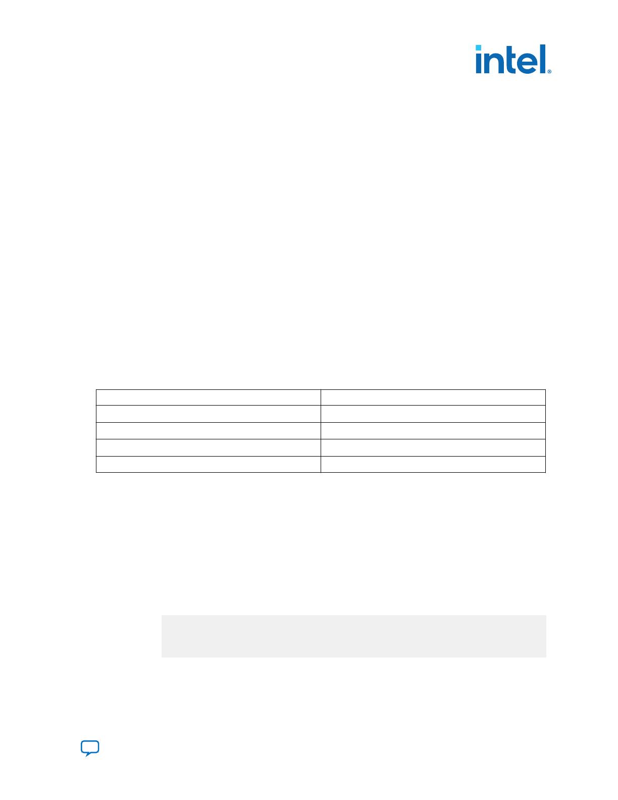
The following table lists the revision name and the revision type for each of the
revisions:
Table 4. Revision Names and Types
Revision Name Revision Type
blinking_led.qsf Partial Reconfiguration - Base
blinking_led_default.qsf Partial Reconfiguration - Persona Implementation
blinking_led_slow.qsf Partial Reconfiguration - Persona Implementation
blinking_led_empty.qsf Partial Reconfiguration - Persona Implementation
Setting the Base Revision Type
1. Click Project Revisions.
2. In Revision Name, select the blinking_led revision, and then click Set Current.
3. Click Apply. The blinking_led revision displays as the current revision.
4. To set the Revision Type for blinking_led, click Assignments Settings
General.
5. For Revision Type, select Partial Reconfiguration - Base, and then click OK.
6. Verify that the blinking_led.qsf now contains the following assignment:
##blinking_led.qsf
set_global_assignment -name REVISION_TYPE PR_BASE
AN 991: Partial Reconfiguration via Configuration Pins (External Host) Reference Design
750856 | 2022.11.14
Send Feedback AN 991: Partial Reconfiguration via Configuration Pins (External Host)
Reference Design: for Intel Agilex F-Series FPGA Development Board
13
Creating Implementation Revisions
1. To open the Revisions dialog box, click Project Revisions.
2. To create a new revision, double-click <<new revision>>.
3. In Revision name, specify blinking_led_default and select blinking_led
for Based on revision.
4. For the Revision type, select Partial Reconfiguration - Persona
Implementation.
Figure 8. Creating Revisions
5. Similarly, set the Revision type for blinking_led_slow and
blinking_led_empty revisions.
6. Verify that each .qsf file now contains the following assignment:
set_global_assignment -name REVISION_TYPE PR_IMPL
set_instance_assignment -name ENTITY_REBINDING \
place_holder -to u_blinking_led
where, place_holder is the default entity name for the newly created PR
implementation revision.
AN 991: Partial Reconfiguration via Configuration Pins (External Host) Reference Design
750856 | 2022.11.14
AN 991: Partial Reconfiguration via Configuration Pins (External Host)
Reference Design: for Intel Agilex F-Series FPGA Development Board Send Feedback
14
Figure 9. Project Revisions
Step 7: Compiling the Base Revision
1. To compile the base revision, click Processing Start Compilation.
Alternatively, the following command compiles the base revision:
quartus_sh --flow compile blinking_led -c blinking_led
2. Inspect the bitstream files that generate in the output_files directory.
Table 5. Generated Files
Name Type Description
blinking_led.sof Base programming file Used for full-chip base configuration
blinking_led.pr_partition.rbf PR bitstream file for base persona Used for partial reconfiguration of base
persona.
blinking_led_static.qdb .qdb database file Finalized database file used to import
the static region.
Related Information
"Floorplan the Partial Reconfiguration Design" in Intel Quartus Prime Pro Edition
User Guide: Partial Reconfiguration
"Applying Floorplan Constraints Incrementally" in Intel Quartus Prime Pro Edition
User Guide: Partial Reconfiguration
Step 8: Preparing PR Implementation Revisions
You must prepare the PR implementation revisions before you can compile and
generate the PR bitstream for device programming. This setup includes adding the
static region .qdb file as the source file for each implementation revision. In addition,
you must specify the corresponding entity of the PR region.
AN 991: Partial Reconfiguration via Configuration Pins (External Host) Reference Design
750856 | 2022.11.14
Send Feedback AN 991: Partial Reconfiguration via Configuration Pins (External Host)
Reference Design: for Intel Agilex F-Series FPGA Development Board
15
1. To set the current revision, click Project Revisions, select
blinking_led_default as the Revision name, and then click Set Current.
2. To verify the correct source for each implementation revision, click Project
Add/Remove Files in Project. The blinking_led.sv file appears in the file
list.
Figure 10. Files Page
3. Repeat steps 1 through 2 to verify the other implementation revision source files:
Implementation Revision Name Source File
blinking_led_default blinking_led.sv
blinking_led_empty blinking_led_empty.sv
blinking_led_slow blinking_led_slow.sv
4. To verify the .qdb file associated with the root partition, click Assignments
Design Partitions Window. Confirm that the Partition Database File specifies
the blinking_led_static.qdb file, or double-click the Partition Database
File cell to specify this file.
Alternatively, the following command assigns this file:
set_instance_assignment -name QDB_FILE_PARTITION \
blinking_led_static.qdb -to |
5. In the Entity Re-binding cell, specify the entity name of each PR partition that
you change in the implementation revision. For the blinking_led_default
implementation revision, the entity name is blinking_led. In this tutorial, you
overwrite the u_blinking_led instance from the base revision compile with the
new blinking_led entity.
Note: A placeholder entity rebinding assignment is added to the implementation
revision automatically. However, you must change the default entity name in
the assignment to an appropriate entity name for your design.
Implementation Revision Name Entity Re-binding
blinking_led_default blinking_led
blinking_led_slow blinking_led_slow
blinking_led_empty blinking_led_empty
AN 991: Partial Reconfiguration via Configuration Pins (External Host) Reference Design
750856 | 2022.11.14
AN 991: Partial Reconfiguration via Configuration Pins (External Host)
Reference Design: for Intel Agilex F-Series FPGA Development Board Send Feedback
16
Figure 11. Entity Rebinding
Verify that each of the following lines now exists in the appropriate .qsf:
##blinking_led_default.qsf
set_instance_assignment -name ENTITY_REBINDING blinking_led \
-to u_blinking_led
##blinking_led_slow.qsf
set_instance_assignment -name ENTITY_REBINDING blinking_led_slow \
-to u_blinking_led
##blinking_led_empty.qsf
set_instance_assignment -name ENTITY_REBINDING blinking_led_empty \
-to u_blinking_led
6. To compile the design, click Processing Start Compilation. Alternatively, the
following command compiles this project:
quartus_sh --flow compile blinking_led –c blinking_led_default
7. Repeat the above steps to prepare blinking_led_slow and
blinking_led_empty revisions:
quartus_sh --flow compile blinking_led –c blinking_led_slow
quartus_sh --flow compile blinking_led –c blinking_led_empty
Note: You can specify any Fitter specific settings that you want to apply during the
PR implementation compilation. Fitter specific settings impact only the fit of
the persona, without affecting the imported static region.
Step 9: Programming the Board
This tutorial uses an Intel Agilex F-Series FPGA development board on the bench,
outside of the PCIe* slot in your host machine. Before you program the board, ensure
that you have completed the following steps:
1. Connect the power supply to the Intel Agilex F-Series FPGA development board.
2. Connect the Intel FPGA Download Cable between your PC USB port and the Intel
FPGA Download Cable port on the development board.
To run the design on the Intel Agilex F-Series FPGA development board:
1. Open the Intel Quartus Prime software and click Tools Programmer.
2. In the Programmer, click Hardware Setup and select USB-Blaster.
3. Click Auto Detect and select the device, AGFB014R24AR0.
4. Click OK. The Intel Quartus Prime software detects and updates the Programmer
with the three FPGA devices on the board.
AN 991: Partial Reconfiguration via Configuration Pins (External Host) Reference Design
750856 | 2022.11.14
Send Feedback AN 991: Partial Reconfiguration via Configuration Pins (External Host)
Reference Design: for Intel Agilex F-Series FPGA Development Board
17
5. Select the AGFB014R24AR0 device, click Change File and load the
blinking_led_default.sof file.
6. Enable Program/Configure for blinking_led_default.sof file.
7. Click Start and wait for the progress bar to reach 100%.
8. Observe the LEDs on the board blinking at the same frequency as the original flat
design.
9. To program only the PR region, right-click the blinking_led_default.sof file
in the Programmer and click Add PR Programming File.
10. Select the blinking_led_slow.pr_partition.rbf file.
11. Disable Program/Configure for blinking_led_default.sof file.
12. Enable Program/Configure for blinking_led_slow.pr_partition.rbf file
and click Start. On the board, observe LED[0] and LED[1] continuing to blink.
When the progress bar reaches 100%, LED[2] and LED[3] blink slower.
13. To reprogram the PR region, right-click the .rbf file in the Programmer and click
Change PR Programing File.
14. Select the .rbf files for the other two personas to observe the behavior on the
board. Loading the blinking_led_default.rbf file causes the LEDs to blink at
a specific frequency, and loading the blinking_led_empty.rbf file causes the
LEDs to stay ON.
Figure 12. Programming the Intel Agilex F-Series FPGA Development Board
Add the .sof file to the device
Add the .rbf file to
program the PR region
Select the .rbf file to
re-program the PR region
AN 991: Partial Reconfiguration via Configuration Pins (External Host) Reference Design
750856 | 2022.11.14
AN 991: Partial Reconfiguration via Configuration Pins (External Host)
Reference Design: for Intel Agilex F-Series FPGA Development Board Send Feedback
18
Hardware Testing Flow
The following sequences describe the reference design hardware testing flow.
Figure 13. Intel Agilex Device External Host Hardware Setup
External Device (Helper FPGA) DUT FPGA
PR RegionSDM
Partial Reconfiguration
External Configuration
Controller Intel FPGA
IP
Your
External
Host
Design
busy
pr_done
pr_error
pr_request
out_clock
Avalon
Streaming
x8,x16,x32
Interface
Step 1: Program the Helper FPGA (External Host)
The following sequence describes programming the helper FPGA that operates as the
PR process external host:
1. Specify the Avalon streaming interface setting that corresponds with the mode
that you select (x8, x16, or x32).
2. Initialize the platform by programming the helper FPGA using the Intel Quartus
Prime Programmer and connected configuration cable.
3. Using the helper FPGA, read the CONF_DONE and AVST_READY signals.
CONF_DONE should be 0, AVST_READY should be 1. Logic high on this pin
indicates the SDM is ready to accept data from an external host. This output is
part of the SDM I/O.
Note: The CONF_DONE pin signals an external host that bitstream transfer is
successful. Use these signals only to monitor the full chip configuration
process. Refer to the Intel Agilex Configuration User Guide for more
information on this pin.
AN 991: Partial Reconfiguration via Configuration Pins (External Host) Reference Design
750856 | 2022.11.14
Send Feedback AN 991: Partial Reconfiguration via Configuration Pins (External Host)
Reference Design: for Intel Agilex F-Series FPGA Development Board
19
Step 2: Program the DUT FPGA with Full Chip SOF via External Host
The following sequence describes programming the DUT FPGA with the full chip SRAM
Object File (.sof) using the host Avalon streaming interface:
1. Write the full chip bitstream into the DDR4 external memory of the helper FPGA
(external host).
2. Configure the DUT FPGA with the full chip .sof using the Avalon streaming
interface (x8, x16, x32).
3. Read the status DUT FPGA configuration signals. CONF_DONE should be 1,
AVST_READY should be 0.
Figure 14. Timing Specifications: Partial Reconfiguration External Controller Intel FPGA
IP
Step 3: Program the DUT FPGA with the First Persona via External Host
1. Apply the freeze on the target PR region in the DUT FPGA.
2. Using the Intel Quartus Prime System Console, assert pr_request to start the
partial reconfiguration. AVST_READY should be 1.
3. Write the first PR persona bitstream into the DDR4 external memory of the helper
FPGA (external host).
4. Using Avalon streaming interface (x8, x16, x32), reconfigure the DUT FPGA with
the first persona bitstream.
5. To monitor the PR status, click Tools System Console to launch System
Console. In System Console, monitor the PR status:
pr_error is 2—reconfiguration in process.
pr_error is 3—reconfiguration is complete.
6. Apply unfreeze on the PR region in the DUT FPGA.
Note: If an error occurs during PR operation, such as failure in version checking or
authorization checking, the PR operation terminates.
Related Information
Intel Agilex Configuration User Guide
Intel Quartus Prime Pro Edition User Guide: Debug Tools
AN 991: Partial Reconfiguration via Configuration Pins (External Host) Reference Design
750856 | 2022.11.14
AN 991: Partial Reconfiguration via Configuration Pins (External Host)
Reference Design: for Intel Agilex F-Series FPGA Development Board Send Feedback
20
  • Page 1 1
  • Page 2 2
  • Page 3 3
  • Page 4 4
  • Page 5 5
  • Page 6 6
  • Page 7 7
  • Page 8 8
  • Page 9 9
  • Page 10 10
  • Page 11 11
  • Page 12 12
  • Page 13 13
  • Page 14 14
  • Page 15 15
  • Page 16 16
  • Page 17 17
  • Page 18 18
  • Page 19 19
  • Page 20 20
  • Page 21 21

Intel 750856 User guide

Type
User guide

Intel 750856, a partial reconfiguration reference design, empowers you to dynamically reconfigure portions of your FPGA while the rest of the design continues operating. Create multiple personas for a specific region without affecting other areas. This methodology shines in systems where various functions share the same FPGA resources. The included Partial Reconfiguration External Configuration Controller IP and simple PR region make it easy to get started. Unleash the flexibility of partial reconfiguration with Intel 750856.

Ask a question and I''ll find the answer in the document

Finding information in a document is now easier with AI