Page is loading ...

EZ-USB NX2LP-Flex™ Flexible USB NAND Flash Controller
CY7C68033/CY7C68034
Cypress Semiconductor Corporation • 198 Champion Court • San Jose, CA 95134-1709 • 408-943-2600
Document #: 001-04247 Rev. *D Revised September 21, 2006
CY7C68033/CY7C68034 Silicon Features
• Certified compliant for Bus- or Self-powered USB 2.0
operation (TID# 40490118)
• Single-chip, integrated USB 2.0 transceiver and smart SIE
• Ultra low power – 43 mA typical current draw in any mode
• Enhanced 8051 core
— Firmware runs from internal RAM, which is downloaded
from NAND flash at startup
— No external EEPROM required
• 15 KBytes of on-chip Code/Data RAM
— Default NAND firmware ~8 kB
— Default free space ~7 kB
• Four programmable BULK/INTERRUPT/ISOCHRONOUS
endpoints
— Buffering options: double, triple, and quad
• Additional programmable (BULK/INTERRUPT) 64-byte
endpoint
• SmartMedia Standard Hardware ECC generation with 1-bit
correction and 2-bit detection
• GPIF (General Programmable Interface)
— Allows direct connection to most parallel interfaces
— Programmable waveform descriptors and configuration
registers to define waveforms
— Supports multiple Ready (RDY) inputs and Control (CTL)
outputs
• 12 fully-programmable GPIO pins
• Integrated, industry-standard enhanced 8051
— 48-MHz, 24-MHz, or 12-MHz CPU operation
— Four clocks per instruction cycle
— Three counter/timers
— Expanded interrupt system
— Two data pointers
• 3.3V operation with 5V tolerant inputs
• Vectored USB interrupts and GPIF/FIFO interrupts
• Separate data buffers for the Set-up and Data portions of a
CONTROL transfer
• Integrated I
2
C™ controller, runs at 100 or 400 kHz
• Four integrated FIFOs
— Integrated glue logic and FIFOs lower system cost
— Automatic conversion to and from 16-bit buses
— Master or slave operation
— Uses external clock or asynchronous strobes
— Easy interface to ASIC and DSP ICs
• Available in space saving, 56-pin QFN package
CY7C68034 Only Silicon Features:
• Ideal for battery powered applications
— Suspend current: 100 μA (typ.)
CY7C68033 Only Silicon Features:
• Ideal for non-battery powered applications
— Suspend current: 300 μA (typ.)
x20
PLL
/0.5
/1.0
/2.0
8051 Core
12/24/48 MHz,
four clocks/cycle
V
CC
1.5k
D+
D–
Address (16)/Data Bus (8)
GPIF
CY
Smart
USB
1.1/2.0
Engine
USB
2.0
XCVR
Additional I/Os
CTL (3)
RDY (2)
8/16
ECC
NAND
Boot Logic
(ROM)
NX2LP-Flex
24 MHz
Ext. Xtal
Connected for
full-speed USB
Integrated full- and
high-speed XCVR
15 kB
RAM
General Programmable
I/F to ASIC/DSP or bus
standards such as 8-bit
NAND, EPP, etc.
4 kB
FIFO
Up to 96 MB/s burst rate
High-performance,
enhanced 8051 core
with low power options
‘Soft Configuration’ enables
easy firmware changes
FIFO and USB endpoint memory
(master or slave modes)
Enhanced USB core
simplifies 8051 code
I
2
C
Master
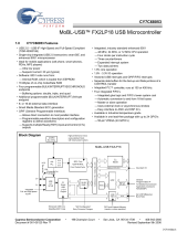
Block Diagram
[+] Feedback

CY7C68033/CY7C68034
Document #: 001-04247 Rev. *D Page 2 of 33
Default NAND Firmware Features
Because the NX2LP-Flex™ is intended for NAND
Flash-based USB mass storage applications, a default
firmware image is included in the development kit with the
following features:
• High (480-Mbps) or full (12-Mbps) speed USB support
• Both common NAND page sizes supported
— 512 bytes for up to 1 Gb capacity
— 2K bytes for up to 8 Gb capacity
• 12 configurable general-purpose I/O (GPIO) pins
— 2 dedicated chip enable (CE#) pins
— 6 configurable CE#/GPIO pins
• Up to 8 NAND Flash single-device (single-die) chips are
supported
• Up to 4 NAND Flash dual-device (dual-die) chips are
supported
• Compile option allows unused CE# pins to be config-
ured as GPIOs
— 4 dedicated GPIO pins
• Industry standard ECC NAND Flash correction
— 1-bit per 256-bit correction
— 2-bit error detection
• Industry standard (SmartMedia) page management for
wear leveling algorithm, bad block handling, and Physical
to Logical management.
• 8-bit NAND Flash interface support
• Support for 30-ns, 50-ns, and 100-ns NAND Flash timing
• Complies with the USB Mass Storage Class Specification
revision 1.0
The default firmware image implements a USB 2.0 NAND
Flash controller. This controller adheres to the Mass Storage
Class Bulk-Only Transport Specification. The USB port of the
NX2LP-Flex is connected to a host computer directly or via the
downstream port of a USB hub. Host software issues
commands and data to the NX2LP-Flex and receives status
and data from the NX2LP-Flex using standard USB protocol.
The default firmware image supports industry leading 8-bit
NAND Flash interfaces and both common NAND page sizes
of 512 and 2k bytes. Up to eight chip enable pins allow the
NX2LP-Flex to be connected to up to eight single- or four
dual-die NAND Flash chips.
Complete source code and documentation for the default
firmware image are included in the NX2LP-Flex development
kit to enable customization for meeting design requirements.
Additionally, compile options for the default firmware allow for
quick configuration of some features to decrease design effort
and increase time-to-market advantages.
Overview
Cypress Semiconductor Corporation’s (Cypress’s) EZ-USB
NX2LP-Flex (CY7C68033/CY7C68034) is a firmware-based,
programmable version of the EZ-USB NX2LP™
(CY7C68023/CY7C68024), which is a fixed-function,
low-power USB 2.0 NAND Flash controller. By integrating the
USB 2.0 transceiver, serial interface engine (SIE), enhanced
8051 microcontroller, and a programmable peripheral
interface in a single chip, Cypress has created a very
cost-effective solution that enables feature-rich NAND
Flash-based applications.
The ingenious architecture of NX2LP-Flex results in USB data
transfer rates of over 53 Mbytes per second, the
maximum-allowable USB 2.0 bandwidth, while still using a
low-cost 8051 microcontroller in a small 56-pin QFN package.
Because it incorporates the USB 2.0 transceiver, the
NX2LP-Flex is more economical, providing a smaller footprint
solution than external USB 2.0 SIE or transceiver implemen-
tations. With EZ-USB NX2LP-Flex, the Cypress Smart SIE
handles most of the USB 1.1 and 2.0 protocol, freeing the
embedded microcontroller for application-specific functions
and decreasing development time while ensuring USB
compatibility.
The General Programmable Interface (GPIF) and
Master/Slave Endpoint FIFO (8- or 16-bit data bus) provide an
easy and glueless interface to popular interfaces such as
UTOPIA, EPP, I
2
C, PCMCIA, and most DSP processors.
Applications
The NX2LP-Flex allows designers to add extra functionality to
basic NAND Flash mass storage designs, or to interface them
with other peripheral devices. Applications may include:
• NAND Flash-based GPS devices
• NAND Flash-based DVB video capture devices
• Wireless pointer/presenter tools with NAND Flash storage
• NAND Flash-based MPEG/TV conversion devices
• Legacy conversion devices with NAND Flash storage
• NAND Flash-based cameras
• NAND Flash mass storage device with biometric (e.g.,
fingerprint) security
• Home PNA devices with NAND Flash storage
• Wireless LAN with NAND Flash storage
• NAND Flash-based MP3 players
• LAN networking with NAND Flash storage
[+] Feedback

CY7C68033/CY7C68034
Document #: 001-04247 Rev. *D Page 3 of 33
Figure 1. Example DVB Block Diagram
Figure 2. Example GPS Block Diagram
The “Reference Designs” section of the Cypress web site
provides additional tools for typical USB 2.0 applications. Each
reference design comes complete with firmware source and
object code, schematics, and documentation. Please visit
http://www.cypress.com for more information.
Functional Overview
USB Signaling Speed
NX2LP-Flex operates at two of the three rates defined in the
USB Specification Revision 2.0, dated April 27, 2000:
• Full speed, with a signaling bit rate of 12 Mbps
• High speed, with a signaling bit rate of 480 Mbps.
NX2LP-Flex does not support the low-speed signaling mode
of 1.5 Mbps.
8051 Microprocessor
The 8051 microprocessor embedded in the NX2LP-Flex has
256 bytes of register RAM, an expanded interrupt system and
three timer/counters.
8051 Clock Frequency
NX2LP-Flex has an on-chip oscillator circuit that uses an
external 24-MHz (±100-ppm) crystal with the following charac-
teristics:
• Parallel resonant
• Fundamental mode
• 500-μW drive level
• 12-pF (5% tolerance) load capacitors.
An on-chip PLL multiplies the 24-MHz oscillator up to
480 MHz, as required by the transceiver/PHY, and internal
counters divide it down for use as the 8051 clock. The default
8051 clock frequency is 12 MHz. The clock frequency of the
8051 can be changed by the 8051 through the CPUCS
register, dynamically
Figure 3. Crystal Configuration.
Special Function Registers
Certain 8051 SFR addresses are populated to provide fast
access to critical NX2LP-Flex functions. These SFR additions
are shown in Table 1. Bold type indicates non-standard,
enhanced 8051 registers. The two SFR rows that end with ‘0’
and ‘8’ contain bit-addressable registers. The four I/O ports
A–D use the SFR addresses used in the standard 8051 for
ports 0–3, which are not implemented in NX2LP-Flex.
Because of the faster and more efficient SFR addressing, the
NX2LP-Flex I/O ports are not addressable in external RAM
space (using the MOVX instruction).
I
2
C Bus
NX2LP supports the I
2
C bus as a master only at 100-/400-kHz.
SCL and SDA pins have open-drain outputs and hysteresis
inputs. These signals must be pulled up to 3.3V, even if no I
2
C
device is connected. The I
2
C bus is disabled at startup and
only available for use after the initial NAND access.
LCD
NX2LP-
Flex
Buttons
DVB
Decoder
NAND Bank(s)
CE[7:0]
CTL
I/O
I/O
D+/-
I/O I/O
NAND-Based
DVB Unit
Audio / Video I/O
NX2LP-
Flex
Buttons
GPS
NAND Bank(s)
CE[7:0]
CTL
I/O
D+/-
I/O I/O
NAND-Based
GPS Unit
LCD
I/O
12 pf
12 pf
24 MHz
20 × PLL
C1
C2
12-pF capacitor values assumes a trace capacitance
of 3 pF per side on a four-layer FR4 PCA
[+] Feedback

CY7C68033/CY7C68034
Document #: 001-04247 Rev. *D Page 4 of 33
Buses
The NX2LP-Flex features an 8- or 16-bit ‘FIFO’ bidirectional
data bus, multiplexed on I/O ports B and D.
The default firmware image implements an 8-bit data bus in
GPIF Master mode. It is recommended that additional inter-
faces added to the default firmware image use this 8-bit data
bus.
Enumeration
During the start-up sequence, internal logic checks for the
presence of NAND Flash with valid firmware. If valid firmware
is found, the NX2LP-Flex loads it and operates according to
the firmware. If no NAND Flash is detected, or if no valid
firmware is found, the NX2LP-Flex uses the default values
from internal ROM space for manufacturing mode operation.
The two modes of operation are described in the section
”Normal Operation Mode” on page 5 and ”Manufacturing
Mode” on page 5.
Table 1. Special Function Registers
x8x 9x Ax Bx CxDxExFx
0
IOA IOB IOC IOD SCON1 PSW ACC B
1SP EXIF INT2CLR IOE SBUF1
2DPL0 MPAGE
INT4CLR OEA
3DPH0
OEB
4 DPL1 OEC
5 DPH1
OED
6 DPS
OEE
7PCON
8 TCON SCON0 IE IP T2CON EICON EIE EIP
9 TMOD SBUF0
ATL0AUTOPTRH1 EP2468STAT EP01STAT RCAP2L
BTL1AUTOPTRL1 EP24FIFOFLGS GPIFTRIG RCAP2H
CTH0RESERVED EP68FIFOFLGS TL2
DTH1AUTOPTRH2 GPIFSGLDATH TH2
E CKCON AUTOPTRL2 GPIFSGLDATLX
F RESERVED AUTOPTRSET-UP GPIFSGLDATLNOX
[+] Feedback

CY7C68033/CY7C68034
Document #: 001-04247 Rev. *D Page 5 of 33
Figure 4. NX2LP-Flex Enumeration Sequence
Normal Operation Mode
In Normal Operation Mode, the NX2LP-Flex behaves as a
USB 2.0 Mass Storage Class NAND Flash controller. This
includes all typical USB device states (powered, configured,
etc.). The USB descriptors are returned according to the data
stored in the configuration data memory area. Normal read
and write access to the NAND Flash is available in this mode.
Manufacturing Mode
In Manufacturing Mode, the NX2LP-Flex enumerates using
the default descriptors and configuration data that are stored
in internal ROM space. This mode allows for first-time
programming of the configuration data memory area, as well
as board-level manufacturing tests.
Default Silicon ID Values
To facilitate proper USB enumeration when no programmed
NAND Flash is present, the NX2LP-Flex has default silicon ID
values stored in ROM space. The default silicon ID values
should only be used for development purposes. Cypress
requires designers to use their own Vendor ID for final
products. A Vendor ID is obtained through registration with the
USB Implementor’s Forum (USB-IF). Also, if the NX2LP-Flex
is used as a mass storage class device, a unique USB serial
number is required for each device in order to comply with the
USB Mass Storage class specification.
Cypress provides all the software tools and drivers necessary
for properly programming and testing the NX2LP-Flex. Please
refer to the documentation in the development kit for more
information on these topics.
ReNumeration™
Cypress’s ReNumeration™ feature is used in conjunction with
the NX2LP-Flex manufacturing software tools to enable
first-time NAND programming. It is only available when used
in conjunction with the NX2LP-Flex Manufacturing tools, and
is not enabled during normal operation.
Bus-powered Applications
The NX2LP-Flex fully supports bus-powered designs by
enumerating with less than 100 mA, as required by the USB
2.0 specification.
Interrupt System
INT2 Interrupt Request and Enable Registers
NX2LP-Flex implements an autovector feature for INT2 and
INT4. There are 27 INT2 (USB) vectors, and 14 INT4
(FIFO/GPIF) vectors. See the EZ-USB Technical Reference
Manual (TRM) for more details.
USB-Interrupt Autovectors
The main USB interrupt is shared by 27 interrupt sources. To
save the code and processing time that normally would be
required to identify the individual USB interrupt source, the
NX2LP-Flex provides a second level of interrupt vectoring,
called Autovectoring. When a USB interrupt is asserted, the
NX2LP-Flex pushes the program counter onto its stack then
jumps to address 0x0500, where it expects to find a ‘jump’
instruction to the USB Interrupt service routine.
Developers familiar with Cypress’s programmable USB
devices should note that these interrupt vector values differ
from those used in other EZ-USB microcontrollers. This is due
to the additional NAND boot logic that is present in the
NX2LP-Flex ROM space. Also, these values are fixed and
cannot be changed in the firmware.
NAND Flash
Programmed?
Load Default
Descriptors and
Configuration Data
Manufacturing
Mode
Load Firmware
From NAND
Enumerate
According To
Firmware
Normal Operation
Mode
Start-up
Enumerate As
Unprogrammed
NX2LP-Flex
NAND Flash
Present?
No
Yes
Yes No
Table 2. Default Silicon ID Values
Default VID/PID/DID
Vendor ID 0x04B4 Cypress Semiconductor
Product ID 0x8613 EZ-USB
®
Default
Device release 0xAnnn Depends on chip revision
(nnn = chip revision, where first
silicon = 001)
[+] Feedback

CY7C68033/CY7C68034
Document #: 001-04247 Rev. *D Page 6 of 33
If Autovectoring is enabled (AV2EN = 1 in the INTSET-UP
register), the NX2LP-Flex substitutes its INT2VEC byte.
Therefore, if the high byte (‘page’) of a jump-table address is
preloaded at location 0x544, the automatically-inserted
INT2VEC byte at 0x545 will direct the jump to the correct
address out of the 27 addresses within the page.
FIFO/GPIF Interrupt (INT4)
Just as the USB Interrupt is shared among 27 individual
USB-interrupt sources, the FIFO/GPIF interrupt is shared
among 14 individual FIFO/GPIF sources. The FIFO/GPIF
Interrupt, like the USB Interrupt, can employ autovectoring.
Table 4 shows the priority and INT4VEC values for the 14
FIFO/GPIF interrupt sources.
Table 3. INT2 USB Interrupts
USB INTERRUPT TABLE FOR INT2
Priority INT2VEC Value Source Notes
1 0x500 SUDAV Setup Data Available
2 0x504 SOF Start of Frame (or microframe)
3 0x508 SUTOK Setup Token Received
4 0x50C SUSPEND USB Suspend request
5 0x510 USB RESET Bus reset
6 0x514 HISPEED Entered high speed operation
7 0x518 EP0ACK NX2LP ACK’d the CONTROL Handshake
8 0x51C Reserved
9 0x520 EP0-IN EP0-IN ready to be loaded with data
10 0x524 EP0-OUT EP0-OUT has USB data
11 0x528 EP1-IN EP1-IN ready to be loaded with data
12 0x52C EP1-OUT EP1-OUT has USB data
13 0x530 EP2 IN: buffer available. OUT: buffer has data
14 0x534 EP4 IN: buffer available. OUT: buffer has data
15 0x538 EP6 IN: buffer available. OUT: buffer has data
16 0x53C EP8 IN: buffer available. OUT: buffer has data
17 0x540 IBN IN-Bulk-NAK (any IN endpoint)
18 0x544 Reserved
19 0x548 EP0PING EP0 OUT was Pinged and it NAK’d
20 0x54C EP1PING EP1 OUT was Pinged and it NAK’d
21 0x550 EP2PING EP2 OUT was Pinged and it NAK’d
22 0x554 EP4PING EP4 OUT was Pinged and it NAK’d
23 0x558 EP6PING EP6 OUT was Pinged and it NAK’d
24 0x55C EP8PING EP8 OUT was Pinged and it NAK’d
25 0x560 ERRLIMIT Bus errors exceeded the programmed limit
26 0x564 Reserved
27 0x568 Reserved
28 0x56C Reserved
29 0x570 EP2ISOERR ISO EP2 OUT PID sequence error
30 0x574 EP4ISOERR ISO EP4 OUT PID sequence error
31 0x578 EP6ISOERR ISO EP6 OUT PID sequence error
32 0x57C EP8ISOERR ISO EP8 OUT PID sequence error
[+] Feedback

CY7C68033/CY7C68034
Document #: 001-04247 Rev. *D Page 7 of 33
If Autovectoring is enabled (AV4EN = 1 in the INTSET-UP
register), the NX2LP-Flex substitutes its INT4VEC byte.
Therefore, if the high byte (‘page’) of a jump-table address is
preloaded at location 0x554, the automatically-inserted
INT4VEC byte at 0x555 will direct the jump to the correct
address out of the 14 addresses within the page. When the
ISR occurs, the NX2LP-Flex pushes the program counter onto
its stack then jumps to address 0x553, where it expects to find
a ‘jump’ instruction to the ISR Interrupt service routine.
Reset and Wakeup
Reset Pin
The input pin RESET#, will reset the NX2LP-Flex when
asserted. This pin has hysteresis and is active LOW. When a
crystal is used as the clock source for the NX2LP-Flex, the
reset period must allow for the stabilization of the crystal and
the PLL. This reset period should be approximately 5 ms after
V
CC
has reached 3.0V. If the crystal input pin is driven by a
clock signal, the internal PLL stabilizes in 200 μs after V
CC
has
reached 3.0V
[1]
. Figure 5 shows a power-on reset condition
and a reset applied during operation. A power-on reset is
defined as the time reset is asserted while power is being
applied to the circuit. A powered reset is defined to be when
the NX2LP-Flex has previously been powered on and
operating and the RESET# pin is asserted.
Cypress provides an application note which describes and
recommends power on reset implementation and can be found
on the Cypress web site. For more information on reset imple-
mentation for the EZ-USB family of products visit the
http://www.cypress.com website.
Table 4. Individual FIFO/GPIF Interrupt Sources
Priority INT4VEC Value Source Notes
1 0x580 EP2PF Endpoint 2 Programmable Flag
2 0x584 EP4PF Endpoint 4 Programmable Flag
3 0x588 EP6PF Endpoint 6 Programmable Flag
4 0x58C EP8PF Endpoint 8 Programmable Flag
5 0x590 EP2EF Endpoint 2 Empty Flag
6 0x594 EP4EF Endpoint 4 Empty Flag
7 0x598 EP6EF Endpoint 6 Empty Flag
8 0x59C EP8EF Endpoint 8 Empty Flag
9 0x5A0 EP2FF Endpoint 2 Full Flag
10 0x5A4 EP4FF Endpoint 4 Full Flag
11 0x5A8 EP6FF Endpoint 6 Full Flag
12 0x5AC EP8FF Endpoint 8 Full Flag
13 0x5B0 GPIFDONE GPIF Operation Complete
14 0x5B4 GPIFWF GPIF Waveform
Note
1. If the external clock is powered at the same time as the CY7C68033/CY7C68034 and has a stabilization wait period, it must be added to the 200 μs.
Figure 5. Reset Timing Plots
V
IL
0V
3.3V
3.0V
T
RESET
V
CC
RESET#
Power-on Reset
T
RESET
V
CC
RESET#
V
IL
Powered Reset
3.3V
0V
[+] Feedback

CY7C68033/CY7C68034
Document #: 001-04247 Rev. *D Page 8 of 33
Wakeup Pins
The 8051 puts itself and the rest of the chip into a power-down
mode by setting PCON.0 = 1. This stops the oscillator and
PLL. When WAKEUP is asserted by external logic, the oscil-
lator restarts, after the PLL stabilizes, and then the 8051
receives a wakeup interrupt. This applies whether or not
NX2LP-Flex is connected to the USB.
The NX2LP-Flex exits the power-down (USB suspend) state
using one of the following methods:
• USB bus activity (if D+/D– lines are left floating, noise on
these lines may indicate activity to the NX2LP-Flex and
initiate a wakeup).
• External logic asserts the WAKEUP pin
• External logic asserts the PA3/WU2 pin.
The second wakeup pin, WU2, can also be configured as a
general purpose I/O pin. This allows a simple external R-C
network to be used as a periodic wakeup source. Note that
WAKEUP is, by default, active LOW.
Program/Data RAM
Internal ROM/RAM Size
The NX2LP-Flex has 1 kBytes ROM and 15 kBytes of internal
program/data RAM, where PSEN#/RD# signals are internally
ORed to allow the 8051 to access it as both program and data
memory. No USB control registers appear in this space.
Internal Code Memory
This mode implements the internal block of RAM (starting at
0x0500) as combined code and data memory, as shown in
Figure 6, below.
Only the internal and scratch pad RAM spaces have the
following access:
• USB download (only supported by the Cypress Manufac-
turing Tool)
• Setup data pointer
• NAND boot access.
Figure 6. Internal Code Memory
Register Addresses
Figure 7. Internal Register Addresses
Table 5. Reset Timing Values
Condition T
RESET
Power-on Reset with crystal 5 ms
Power-on Reset with external
clock source
200 μs + Clock stability time
Powered Reset 200 μs
*SUDPTR, USB download, NAND boot access
FFFF
E200
E1FF
E000
3FFF
0000
7.5 kBytes
USB registers
and 4 kBytes
FIFO buffers
(RD#, WR#)
512 Bytes RAM Data
(RD#, WR#)*
15 kBytes RAM
Code and Data
(PSEN#, RD#,
WR#)*
0500
1 kbyte ROM
FFFF
E800
E7BF
E740
E73F
E700
E6FF
E500
E4FF
E480
E47F
E400
E200
E1FF
E000
E3FF
EFFF
2 KBytes RESERVED
64 Bytes EP0 IN/OUT
64 Bytes RESERVED
8051 Addressable Registers
Reserved (128)
128 bytes GPIF Waveforms
512 bytes
8051 xdata RAM
F000
(512)
Reserved (512)
E780
64 Bytes EP1OUT
E77F
64 Bytes EP1IN
E7FF
E7C0
4 KBytes EP2-EP8
buffers
(8 x 512)
[+] Feedback

CY7C68033/CY7C68034
Document #: 001-04247 Rev. *D Page 9 of 33
Endpoint RAM
Size
• 3 × 64 bytes (Endpoints 0 and 1)
• 8 × 512 bytes (Endpoints 2, 4, 6, 8)
Organization
• EP0
— Bidirectional endpoint zero, 64-byte buffer
• EP1IN, EP1OUT
— 64-byte buffers, bulk or interrupt
• EP2,4,6,8
— Eight 512-byte buffers, bulk, interrupt, or isochronous.
— EP4 and EP8 can be double buffered, while EP2 and 6
can be either double, triple, or quad buffered.
For high-speed endpoint configuration options, see Figure 8.
Setup Data Buffer
A separate 8-byte buffer at 0xE6B8-0xE6BF holds the setup
data from a CONTROL transfer.
Endpoint Configurations (High-speed Mode)
Endpoints 0 and 1 are the same for every configuration.
Endpoint 0 is the only CONTROL endpoint, and endpoint 1 can
be either BULK or INTERRUPT. The endpoint buffers can be
configured in any 1 of the 12 configurations shown in the
vertical columns. When operating in full-speed BULK mode,
only the first 64 bytes of each buffer are used. For example, in
high-speed the max packet size is 512 bytes, but in full-speed
it is 64 bytes. Even though a buffer is configured to be a 512
byte buffer, in full-speed only the first 64 bytes are used. The
unused endpoint buffer space is not available for other opera-
tions. An example endpoint configuration would be:
EP2–1024 double buffered; EP6–512 quad buffered
(column 8 in Figure 8).
Figure 8. Endpoint Configuration
Default Full-Speed Alternate Settings
64
64
64
512
512
1024
1024
1024
1024
1024
1024
1024
512
512
512
512
512
512
512
512
512
512
EP2
EP2
EP2
EP6
EP6
EP8
EP8
EP0 IN&OUT
EP1 IN
EP1 OUT
1024
1024
EP6
1024
512
512
EP8
512
512
EP6
512
512
512
512
EP2
512
512
EP4
512
512
EP2
512
512
EP4
512
512
EP2
512
512
EP4
512
512
EP2
512
512
512
512
EP2
512
512
512
512
EP2
512
512
1024
EP2
1024
1024
EP2
1024
1024
EP2
1024
512
512
EP6
1024
1024
EP6
512
512
EP8
512
512
EP6
512
512
512
512
EP6
1024
1024
EP6
512
512
EP8
512
512
EP6
512
512
64
64
64
64
64
64
64
64
64
64
64
64
64
64
64
64
64
64
64
64
64
64
64
64
64
64
64
64
64
64
64
64
64
1
2
3
4
5
6
7
8
9
10
11
12
Table 6. Default Full-Speed Alternate Settings
[2, 3]
Alternate Setting 0 1 2 3
ep0 64 64 64 64
ep1out 0 64 bulk 64 int 64 int
ep1in 0 64 bulk 64 int 64 int
ep2 0 64 bulk out (2×) 64 int out (2×) 64 iso out (2×)
Notes
2. ‘0’ means ‘not implemented.’
3. ‘2×’ means ‘double buffered.’
[+] Feedback

CY7C68033/CY7C68034
Document #: 001-04247 Rev. *D Page 10 of 33
Default High-Speed Alternate Settings
External FIFO Interface
Architecture
The NX2LP-Flex slave FIFO architecture has eight 512-byte
blocks in the endpoint RAM that directly serve as FIFO
memories, and are controlled by FIFO control signals (such as
SLCS#, SLRD, SLWR, SLOE, PKTEND, and flags).
In operation, some of the eight RAM blocks fill or empty from
the SIE, while the others are connected to the I/O transfer
logic. The transfer logic takes two forms, the GPIF for internally
generated control signals, or the slave FIFO interface for
externally controlled transfers.
Master/Slave Control Signals
The NX2LP-Flex endpoint FIFOS are implemented as eight
physically distinct 256x16 RAM blocks. The 8051/SIE can
switch any of the RAM blocks between two domains, the USB
(SIE) domain and the 8051-I/O Unit domain. This switching is
done virtually instantaneously, giving essentially zero transfer
time between ‘USB FIFOS’ and ‘Slave FIFOS.’ Since they are
physically the same memory, no bytes are actually transferred
between buffers.
At any given time, some RAM blocks are filling/emptying with
USB data under SIE control, while other RAM blocks are
available to the 8051 and/or the I/O control unit. The RAM
blocks operate as single-port in the USB domain, and
dual-port in the 8051-I/O domain. The blocks can be
configured as single, double, triple, or quad buffered as previ-
ously shown.
The I/O control unit implements either an internal-master (M
for master) or external-master (S for Slave) interface.
In Master (M) mode, the GPIF internally controls
FIFOADR[1:0] to select a FIFO. The two RDY pins can be
used as flag inputs from an external FIFO or other logic if
desired. The GPIF can be run from an internally derived clock
(IFCLK), at a rate that transfers data up to 96 Megabytes/s
(48-MHz IFCLK with 16-bit interface).
In Slave (S) mode, the NX2LP-Flex accepts an internally
derived clock (IFCLK, max. frequency 48 MHz) and SLCS#,
SLRD, SLWR, SLOE, PKTEND signals from external logic.
Each endpoint can individually be selected for byte or word
operation by an internal configuration bit, and a Slave FIFO
Output Enable signal SLOE enables data of the selected
width. External logic must ensure that the output enable signal
is inactive when writing data to a slave FIFO. The slave
interface must operate asynchronously, where the SLRD and
SLWR signals act directly as strobes, rather than a clock
qualifier as in a synchronous mode. The signals SLRD, SLWR,
SLOE and PKTEND are gated by the signal SLCS#.
GPIF and FIFO Clock Rates
An 8051 register bit selects one of two frequencies for the
internally supplied interface clock: 30 MHz and 48 MHz. A bit
within the IFCONFIG register will invert the IFCLK signal.
The default NAND firmware image implements a 48-MHz
internally supplied interface clock. The NAND boot logic uses
the same configuration to implement 100-ns timing on the
NAND bus to support proper detection of all NAND Flash
types.
GPIF
The GPIF is a flexible 8- or 16-bit parallel interface driven by a
user-programmable finite state machine. It allows the
NX2LP-Flex to perform local bus mastering, and can
implement a wide variety of protocols such as 8-bit NAND
interface, printer parallel port, and Utopia. The default NAND
firmware and boot logic utilizes GPIF functionality to interface
with NAND Flash.
The GPIF on the NX2LP-Flex features three programmable
control outputs (CTL) and two general-purpose ready inputs
(RDY). The GPIF data bus width can be 8 or 16 bits. Because
ep4 0 64 bulk out (2×) 64 bulk out (2×) 64 bulk out (2×)
ep6 0 64 bulk in (2×) 64 int in (2×) 64 iso in (2×)
ep8 0 64 bulk in (2×) 64 bulk in (2×) 64 bulk in (2×)
Table 6. Default Full-Speed Alternate Settings
[2, 3]
(continued)
Note
4. Even though these buffers are 64 bytes, they are reported as 512 for USB 2.0 compliance. The user must never transfer packets larger than 64 bytes to EP1.
Table 7. Default High-Speed Alternate Settings
[2, 3]
Alternate Setting 0 1 2 3
ep0 64 64 64 64
ep1out 0 512 bulk
[4]
64 int 64 int
ep1in 0 512 bulk
[4]
64 int 64 int
ep2 0 512 bulk out (2×) 512 int out (2×) 512 iso out (2×)
ep4 0 512 bulk out (2×) 512 bulk out (2×) 512 bulk out (2×)
ep6 0 512 bulk in (2×) 512 int in (2×) 512 iso in (2×)
ep8 0 512 bulk in (2×) 512 bulk in (2×) 512 bulk in (2×)
[+] Feedback

CY7C68033/CY7C68034
Document #: 001-04247 Rev. *D Page 11 of 33
the default NAND firmware image implements an 8-bit data
bus and up to 8 chip enable pins on the GPIF ports, it is recom-
mended that designs based upon the default firmware image
use an 8-bit data bus as well.
Each GPIF vector defines the state of the control outputs, and
determines what state a ready input (or multiple inputs) must
be before proceeding. The GPIF vector can be programmed
to advance a FIFO to the next data value, advance an address,
etc. A sequence of the GPIF vectors make up a single
waveform that will be executed to perform the desired data
move between the NX2LP-Flex and the external device.
Three Control OUT Signals
The NX2LP-Flex exposes three control signals, CTL[2:0].
CTLx waveform edges can be programmed to make transi-
tions as fast as once per clock (20.8 ns using a 48-MHz clock).
Two Ready IN Signals
The 8051 programs the GPIF unit to test the RDY pins for
GPIF branching. The 56-pin package brings out two signals,
RDY[1:0].
Long Transfer Mode
In GPIF Master mode, the 8051 appropriately sets GPIF trans-
action count registers (GPIFTCB3, GPIFTCB2, GPIFTCB1, or
GPIFTCB0) for unattended transfers of up to 2
32
transactions.
The GPIF automatically throttles data flow to prevent under- or
over-flow until the full number of requested transactions
complete. The GPIF decrements the value in these registers
to represent the current status of the transaction.
ECC Generation
[5]
The NX2LP-Flex can calculate ECCs (Error-Correcting
Codes) on data that passes across its GPIF or Slave FIFO
interfaces. There are two ECC configurations:
• Two ECCs, each calculated over 256 bytes (SmartMedia
Standard)
• One ECC calculated over 512 bytes.
The two ECC configurations described below are selected by
the ECCM bit. The ECC can correct any one-bit error or detect
any two-bit error.
ECCM = 0
Two 3-byte ECCs, each calculated over a 256-byte block of
data. This configuration conforms to the SmartMedia Standard
and is used by both the NAND boot logic and default NAND
firmware image.
When any value is written to ECCRESET and data is then
passed across the GPIF or Slave FIFO interface, the ECC for
the first 256 bytes of data will be calculated and stored in
ECC1. The ECC for the next 256 bytes of data will be stored
in ECC2. After the second ECC is calculated, the values in the
ECCx registers will not change until ECCRESET is written
again, even if more data is subsequently passed across the
interface.
ECCM = 1
One 3-byte ECC calculated over a 512-byte block of data.
When any value is written to ECCRESET and data is then
passed across the GPIF or Slave FIFO interface, the ECC for
the first 512 bytes of data will be calculated and stored in
ECC1; ECC2 is unused. After the ECC is calculated, the value
in ECC1 will not change until ECCRESET is written again,
even if more data is subsequently passed across the interface
Autopointer Access
NX2LP-Flex provides two identical autopointers. They are
similar to the internal 8051 data pointers, but with an additional
feature: they can optionally increment after every memory
access. Also, the autopointers can point to any NX2LP-Flex
register or endpoint buffer space.
I
2
C Controller
NX2LP has one I
2
C port that the 8051, once running uses to
control external I
2
C devices. The I
2
C port operates in master
mode only. The I
2
C post is disabled at startup and only
available for use after the initial NAND access.
I
2
C Port Pins
The I
2
C pins SCL and SDA must have external 2.2-kΩ pull-up
resistors even if no EEPROM is connected to the NX2LP.
I
2
C Interface General-Purpose Access
The 8051 can control peripherals connected to the I
2
C bus
using the I
2
CTL and I
2
DATA registers. NX2LP provides I
2
C
master control only and is never an I
2
C slave.
Note
5. To use the ECC logic, the GPIF or Slave FIFO interface must be configured for byte-wide operation.
[+] Feedback

CY7C68033/CY7C68034
Document #: 001-04247 Rev. *D Page 12 of 33
Pin Assignments
Figure 9 and Figure 10 identify all signals for the 56-pin
NX2LP-Flex package.
Three modes of operation are available for the NX2LP-Flex:
Port mode, GPIF Master mode, and Slave FIFO mode. These
modes define the signals on the right edge of each column in
Figure 9. The right-most column details the signal functionality
from the default NAND firmware image, which actually utilizes
GPIF Master mode. The signals on the left edge of the ‘Port’
column are common to all modes of the NX2LP-Flex. The
8051 selects the interface mode using the IFCONFIG[1:0]
register bits. Port mode is the power-on default configuration.
Figure 10 details the pinout of the 56-pin package and lists pin
names for all modes of operation. Pin names with an asterisk
(*) feature programmable polarity.
Figure 9. Port and Signal Mapping
XTALIN
XTALOUT
RESET#
WAKEUP#
SCL
SDATA
DPLUS
DMINUS
→ RDY0
→ RDY1
← CTL0
← CTL1
← CTL2
↔ PA7
↔ PA6
↔ PA5
↔ PA4
↔ PA3/WU2
↔ PA2
↔ PA1/INT1#
↔ PA0/INT0#
↔ GPIO8
← GPIO9
↔ FD[15]
↔ FD[14]
↔ FD[13]
↔ FD[12]
↔ FD[11]
↔ FD[10]
↔ FD[9]
↔ FD[8]
↔ FD[7]
↔ FD[6]
↔ FD[5]
↔ FD[4]
↔ FD[3]
↔ FD[2]
↔ FD[1]
↔ FD[0]
→ SLRD
→ SLWR
← FLAGA
← FLAGB
← FLAGC
↔ FLAGD/SLCS#/PA7
↔ PKTEND
← FIFOADR1
↔ FIFOADR0
← PA3/WU2
← SLOE
← PA1/INT1#
↔ PA0/INT0#
↔ GPIO8
← GPIO9
↔ FD[15]
↔ FD[14]
↔ FD[13]
↔ FD[12]
↔ FD[11]
↔ FD[10]
↔ FD[9]
↔ FD[8]
↔ FD[7]
↔ FD[6]
↔ FD[5]
↔ FD[4]
↔ FD[3]
↔ FD[2]
↔ FD[1]
↔ FD[0]
PD7
PD6
PD5
PD4
PD3
PD2
PD1
PD0
PB7
PB6
PB5
PB4
PB3
PB2
PB1
PB0
PA7
PA6
PA5
PA4
WU2/PA3
PA2
INT1#/PA1
INTO#/PA0
GPIO8
GPIO9
Port GPIF Master Slave FIFO
Default NAND
↔ CE7#/GPIO7
↔ CE6#/GPIO6
↔ CE5#/GPIO5
↔ CE4#/GPIO4
↔ CE3#/GPIO3
↔ CE2#/GPIO2
↔ CE1#
↔ CE0#
↔ DD7
↔ DD6
↔ DD5
↔ DD4
↔ DD3
↔ DD2
↔ DD1
↔ DD0
→ R_B1#
→ R_B2#
← WE#
← RE0#
← RE1#
← GPIO1
← GPIO0
← WP_SW#
← WP_NF#
← LED2#
→ LED1#
↔ ALE
↔ CLE
↔ GPIO8
← GPIO9
Firmware Use
[+] Feedback

CY7C68033/CY7C68034
Document #: 001-04247 Rev. *D Page 13 of 33
Figure 10. CY7C68033/CY7C68034 56-pin QFN Pin Assignment
CY7C68033/CY7C68034
56-pin QFN
28
27
26
25
24
23
22
21
20
19
18
17
16
15
43
44
45
46
47
48
49
50
51
52
53
54
55
56
1
2
3
4
5
6
7
8
9
10
11
12
13
14
42
41
40
39
38
37
36
35
34
33
32
31
30
29
RESET#
GND
PA7/*FLAGD/SLCS#
PA6/*PKTEND
PA5/FIFOADR1
PA4/FIFOADR0
PA3/*WU2
PA2/*SLOE
PA1/INT1#
PA0/INT0#
VCC
CTL2/*FLAGC
CTL1/*FLAGB
CTL0/*FLAGA
RDY0/*SLRD
RDY1/*SLWR
AVCC
XTALOUT
XTALIN
AGND
AVCC
DPLUS
DMINUS
AGND
VCC
GND
GPIO8
RESERVED#
VCC
*WAKEUP
PD0/FD8
PD1/FD9
PD2/FD10
PD3/FD11
PD4/FD12
PD5/FD13
PD6/FD14
PD7/FD15
GND
GPIO9
VCC
GND
GND
VCC
GND
PB7/FD7
PB6/FD6
PB5/FD5
PB4/FD4
PB3/FD3
PB2/FD2
PB1/FD1
PB0/FD0
VCC
SDATA
SCL
[+] Feedback

CY7C68033/CY7C68034
Document #: 001-04247 Rev. *D Page 14 of 33
Table 8. NX2LP-Flex Pin Descriptions
[6]
56 QFN
Pin
Number
Default Pin
Name
NAND
Firmware
Usage
Pin
Type
Default
State
Description
9 DMINUS N/A I/O/Z Z USB D– Signal. Connect to the USB D– signal.
8 DPLUS N/A I/O/Z Z USB D+ Signal. Connect to the USB D+ signal.
42 RESET# N/A Input N/A Active LOW Reset. Resets the entire chip. See section ”Reset and
Wakeup” on page 7 for more details.
5 XTALIN N/A Input N/A Crystal Input. Connect this signal to a 24-MHz parallel-resonant,
fundamental mode crystal and load capacitor to GND.
It is also correct to drive XTALIN with an external 24-MHz square
wave derived from another clock source. When driving from an
external source, the driving signal should be a 3.3V square wave.
4 XTALOUT N/A Output N/A Crystal Output. Connect this signal to a 24-MHz parallel-resonant,
fundamental mode crystal and load capacitor to GND.
If an external clock is used to drive XTALIN, leave this pin open.
54 GPIO9 GPIO9 O/Z 12 MHz GPIO9 is a bidirectional IO port pin.
1 RDY0 or
SLRD
R_B1# Input N/A Multiplexed pin whose function is selected by IFCONFIG[1:0].
RDY0 is a GPIF input signal.
SLRD is the input-only read strobe with programmable polarity
(FIFOPINPOLAR[3]) for the slave FIFOs connected to FD[7:0] or
FD[15:0].
R_B1# is a NAND Ready/Busy input signal.
2 RDY1 or
SLWR
R_B2# Input N/A Multiplexed pin whose function is selected by IFCONFIG[1:0].
RDY1 is a GPIF input signal.
SLWR is the input-only write strobe with programmable polarity
(FIFOPINPOLAR[2]) for the slave FIFOs connected to FD[7:0] or
FD[15:0].
R_B2# is a NAND Ready/Busy input signal.
29 CTL0 or
FLAGA
WE# O/Z H Multiplexed pin whose function is selected by IFCONFIG[1:0].
CTL0 is a GPIF control output.
FLAGA is a programmable slave-FIFO output status flag signal.
Defaults to programmable for the FIFO selected by the
FIFOADR[1:0] pins.
WE# is the NAND write enable output signal.
30 CTL1 or
FLAGB
RE0# O/Z H Multiplexed pin whose function is selected by IFCONFIG[1:0].
CTL1 is a GPIF control output.
FLAGB is a programmable slave-FIFO output status flag signal.
Defaults to FULL for the FIFO selected by the FIFOADR[1:0] pins.
RE0# is a NAND read enable output signal.
31 CTL2 or
FLAGC
RE1# O/Z H Multiplexed pin whose function is selected by IFCONFIG[1:0].
CTL2 is a GPIF control output.
FLAGC is a programmable slave-FIFO output status flag signal.
Defaults to EMPTY for the FIFO selected by the FIFOADR[1:0] pins.
RE1# is a NAND read enable output signal.
Note
6. Unused inputs should not be left floating. Tie either HIGH or LOW as appropriate. Outputs should only be pulled up or down to ensure signals at power-up and i
n
standby. Note also that no pins should be driven while the device is powered down.
[+] Feedback

CY7C68033/CY7C68034
Document #: 001-04247 Rev. *D Page 15 of 33
13 GPIO8 GPIO8 I/O/Z I GPIO8: is a bidirectional IO port pin.
14 Reserved# N/A Input N/A Reserved. Connect to ground.
15 SCL N/A OD Z Clock for the I
2
C interface. Connect to VCC with a 2.2K resistor,
even if no I
2
C peripheral is attached.
16 SDATA N/A OD Z Data for the I
2
C interface. Connect to VCC with a 2.2K resistor, even
if no I
2
C peripheral is attached.
44 WAKEUP Unused Input N/A USB Wakeup. If the 8051 is in suspend, asserting this pin starts up
the oscillator and interrupts the 8051 to allow it to exit the suspend
mode. Holding WAKEUP asserted inhibits the EZ-USB chip from
suspending. This pin has programmable polarity, controlled by
WAKEUP[4].
Port A
33 PA0 or
INT0#
CLE I/O/Z I
(PA0)
Multiplexed pin whose function is selected by PORTACFG[0]
PA0 is a bidirectional IO port pin.
INT0# is the active-LOW 8051 INT0 interrupt input signal, which is
either edge triggered (IT0 = 1) or level triggered (IT0 = 0).
CLE is the NAND Command Latch Enable signal.
34 PA1 or
INT1#
ALE I/O/Z I
(PA1)
Multiplexed pin whose function is selected by PORTACFG[1]
PA1 is a bidirectional IO port pin.
INT1# is the active-LOW 8051 INT1 interrupt input signal, which is
either edge triggered (IT1 = 1) or level triggered (IT1 = 0).
ALE is the NAND Address Latch Enable signal.
35 PA2 or
SLOE
LED1# I/O/Z I
(PA2)
Multiplexed pin whose function is selected by IFCONFIG[1:0].
PA2 is a bidirectional IO port pin.
SLOE is an input-only output enable with programmable polarity
(FIFOPINPOLAR[4]) for the slave FIFOs connected to FD[7:0] or
FD[15:0].
LED1# is the data activity indicator LED sink pin.
36 PA3 or
WU2
LED2# I/O/Z I
(PA3)
Multiplexed pin whose function is selected by WAKEUP[7] and
OEA[3]
PA3 is a bidirectional I/O port pin.
WU2 is an alternate source for USB Wakeup, enabled by WU2EN
bit (WAKEUP[1]) and polarity set by WU2POL (WAKEUP[4]). If the
8051 is in suspend and WU2EN = 1, a transition on this pin starts
up the oscillator and interrupts the 8051 to allow it to exit the suspend
mode. Asserting this pin inhibits the chip from suspending, if
WU2EN = 1.
LED2# is the chip activity indicator LED sink pin.
37 PA4 or
FIFOADR0
WP_NF# I/O/Z I
(PA4)
Multiplexed pin whose function is selected by IFCONFIG[1:0].
PA4 is a bidirectional I/O port pin.
FIFOADR0 is an input-only address select for the slave FIFOs
connected to FD[7:0] or FD[15:0].
WP_NF# is the NAND write-protect control output signal.
38 PA5 or
FIFOADR1
WP_SW# I/O/Z I
(PA5)
Multiplexed pin whose function is selected by IFCONFIG[1:0].
PA5 is a bidirectional I/O port pin.
FIFOADR1 is an input-only address select for the slave FIFOs
connected to FD[7:0] or FD[15:0].
WP_SW# is the NAND write-protect switch input signal.
Table 8. NX2LP-Flex Pin Descriptions (continued)
[6]
56 QFN
Pin
Number
Default Pin
Name
NAND
Firmware
Usage
Pin
Type
Default
State
Description
[+] Feedback

CY7C68033/CY7C68034
Document #: 001-04247 Rev. *D Page 16 of 33
39 PA6 or
PKTEND
GPIO0
(Input)
I/O/Z I
(PA6)
Multiplexed pin whose function is selected by the IFCONFIG[1:0]
bits.
PA6 is a bidirectional I/O port pin.
PKTEND is an input used to commit the FIFO packet data to the
endpoint and whose polarity is programmable via FIFOPIN-
POLAR[5].
GPIO1 is a general purpose I/O signal.
40 PA7 or
FLAGD or
SLCS#
GPIO1
(Input)
I/O/Z I
(PA7)
Multiplexed pin whose function is selected by the IFCONFIG[1:0]
and PORTACFG[7] bits.
PA7 is a bidirectional I/O port pin.
FLAGD is a programmable slave-FIFO output status flag signal.
SLCS# gates all other slave FIFO enable/strobes
GPIO0 is a general purpose I/O signal.
Port B
18 PB0 or
FD[0]
DD0 I/O/Z I
(PB0)
Multiplexed pin whose function is selected by IFCONFIG[1:0].
PB0 is a bidirectional I/O port pin.
FD[0] is the bidirectional FIFO/GPIF data bus.
DD0 is a bidirectional NAND data bus signal.
19 PB1 or
FD[1]
DD1 I/O/Z I
(PB1)
Multiplexed pin whose function is selected by IFCONFIG[1:0].
PB1 is a bidirectional I/O port pin.
FD[1] is the bidirectional FIFO/GPIF data bus.
DD1 is a bidirectional NAND data bus signal.
20 PB2 or
FD[2]
DD2 I/O/Z I
(PB2)
Multiplexed pin whose function is selected by IFCONFIG[1:0].
PB2 is a bidirectional I/O port pin.
FD[2] is the bidirectional FIFO/GPIF data bus.
DD2 is a bidirectional NAND data bus signal.
21 PB3 or
FD[3]
DD3 I/O/Z I
(PB3)
Multiplexed pin whose function is selected by IFCONFIG[1:0].
PB3 is a bidirectional I/O port pin.
FD[3] is the bidirectional FIFO/GPIF data bus.
DD3 is a bidirectional NAND data bus signal.
22 PB4 or
FD[4]
DD4 I/O/Z I
(PB4)
Multiplexed pin whose function is selected by IFCONFIG[1:0].
PB4 is a bidirectional I/O port pin.
FD[4] is the bidirectional FIFO/GPIF data bus.
DD4 is a bidirectional NAND data bus signal.
23 PB5 or
FD[5]
DD5 I/O/Z I
(PB5)
Multiplexed pin whose function is selected by IFCONFIG[1:0].
PB5 is a bidirectional I/O port pin.
FD[5] is the bidirectional FIFO/GPIF data bus.
DD5 is a bidirectional NAND data bus signal.
24 PB6 or
FD[6]
DD6 I/O/Z I
(PB6)
Multiplexed pin whose function is selected by IFCONFIG[1:0].
PB6 is a bidirectional I/O port pin.
FD[6] is the bidirectional FIFO/GPIF data bus.
DD6 is a bidirectional NAND data bus signal.
25 PB7 or
FD[7]
DD7 I/O/Z I
(PB7)
Multiplexed pin whose function is selected by IFCONFIG[1:0].
PB7 is a bidirectional I/O port pin.
FD[7] is the bidirectional FIFO/GPIF data bus.
DD7 is a bidirectional NAND data bus signal.
PORT D
45 PD0 or
FD[8]
CE0# I/O/Z I
(PD0)
Multiplexed pin whose function is selected by the IFCONFIG[1:0]
and EPxFIFOCFG.0 (wordwide) bits.
FD[8] is the bidirectional FIFO/GPIF data bus.
CE0# is a NAND chip enable output signal.
Table 8. NX2LP-Flex Pin Descriptions (continued)
[6]
56 QFN
Pin
Number
Default Pin
Name
NAND
Firmware
Usage
Pin
Type
Default
State
Description
[+] Feedback

CY7C68033/CY7C68034
Document #: 001-04247 Rev. *D Page 17 of 33
46 PD1 or
FD[9]
CE1# I/O/Z I
(PD1)
Multiplexed pin whose function is selected by the IFCONFIG[1:0]
and EPxFIFOCFG.0 (wordwide) bits.
FD[9] is the bidirectional FIFO/GPIF data bus.
CE1# is a NAND chip enable output signal.
47 PD2 or
FD[10]
CE2# or GPIO2 I/O/Z I
(PD2)
Multiplexed pin whose function is selected by the IFCONFIG[1:0]
and EPxFIFOCFG.0 (wordwide) bits.
FD[10] is the bidirectional FIFO/GPIF data bus.
CE2# is a NAND chip enable output signal.
GPIO2 is a general purpose I/O signal.
48 PD3 or
FD[11]
CE3# or GPIO3 I/O/Z I
(PD3)
Multiplexed pin whose function is selected by the IFCONFIG[1:0]
and EPxFIFOCFG.0 (wordwide) bits.
FD[11] is the bidirectional FIFO/GPIF data bus.
CE3# is a NAND chip enable output signal.
GPIO3 is a general purpose I/O signal.
49 PD4 or
FD[12]
CE4# or GPIO4 I/O/Z I
(PD4)
Multiplexed pin whose function is selected by the IFCONFIG[1:0]
and EPxFIFOCFG.0 (wordwide) bits.
FD[12] is the bidirectional FIFO/GPIF data bus.
CE4# is a NAND chip enable output signal.
GPIO4 is a general purpose I/O signal.
50 PD5 or
FD[13]
CE5# or GPIO5 I/O/Z I
(PD5)
Multiplexed pin whose function is selected by the IFCONFIG[1:0]
and EPxFIFOCFG.0 (wordwide) bits.
FD[13] is the bidirectional FIFO/GPIF data bus.
CE5# is a NAND chip enable output signal.
GPIO5 is a general purpose I/O signal.
51 PD6 or
FD[14]
CE6# or GPIO6 I/O/Z I
(PD6)
Multiplexed pin whose function is selected by the IFCONFIG[1:0]
and EPxFIFOCFG.0 (wordwide) bits.
FD[14] is the bidirectional FIFO/GPIF data bus.
CE6# is a NAND chip enable output signal.
GPIO6 is a general purpose I/O signal.
52 PD7 or
FD[15]
CE7# or GPIO7 I/O/Z I
(PD7)
Multiplexed pin whose function is selected by the IFCONFIG[1:0]
and EPxFIFOCFG.0 (wordwide) bits.
FD[15] is the bidirectional FIFO/GPIF data bus.
CE7# is a NAND chip enable output signal.
GPIO7 is a general purpose I/O signal.
Power and Ground
3
7
AVCC N/A Power N/A Analog V
CC
. Connect this pin to 3.3V power source. This signal
provides power to the analog section of the chip.
6
10
AGND N/A Ground N/A Analog Ground. Connect to ground with as short a path as
possible.
11
17
27
32
43
55
VCC N/A Power N/A V
CC
. Connect to 3.3V power source.
12
26
28
41
53
56
GND N/A Ground N/A Ground.
Table 8. NX2LP-Flex Pin Descriptions (continued)
[6]
56 QFN
Pin
Number
Default Pin
Name
NAND
Firmware
Usage
Pin
Type
Default
State
Description
[+] Feedback

CY7C68033/CY7C68034
Document #: 001-04247 Rev. *D Page 18 of 33
Register Summary
NX2LP-Flex register bit definitions are described in the EZ-USB TRM in greater detail. Some registers that are listed here and in
the TRM do not apply to the NX2LP-Flex. They are kept here for consistency reasons only. Registers that do not apply to the
NX2LP-Flex should be left at their default power-up values.
Table 9. NX2LP-Flex Register Summary
Hex Size Name Description b7 b6 b5 b4 b3 b2 b1 b0 Default Access
GPIF Waveform Memories
E400 128 WAVEDATA GPIF Waveform
Descriptor 0, 1, 2, 3 data
D7 D6 D5 D4 D3 D2 D1 D0 xxxxxxxx RW
E480 128 reserved
GENERAL CONFIGURATION
E50D GPCR2 General Purpose Configu-
ration Register 2
reserved reserved reserved FULL_SPEE
D_ONLY
reserved reserved reserved reserved 00000000 R
E600 1 CPUCS CPU Control & Status 0 0 PORTCSTB CLKSPD1 CLKSPD0 CLKINV CLKOE 8051RES 00000010 rrbbbbbr
E601 1 IFCONFIG Interface Configuration
(Ports, GPIF, slave FIFOs)
1 3048MHZ 0 IFCLKPOL ASYNC GSTATE IFCFG1 IFCFG0 10000000 RW
E602 1 PINFLAGSAB
[7]
Slave FIFO FLAGA and
FLAGB Pin Configuration
FLAGB3 FLAGB2 FLAGB1 FLAGB0 FLAGA3 FLAGA2 FLAGA1 FLAGA0 00000000 RW
E603 1 PINFLAGSCD
[7]
Slave FIFO FLAGC and
FLAGD Pin Configuration
FLAGD3 FLAGD2 FLAGD1 FLAGD0 FLAGC3 FLAGC2 FLAGC1 FLAGC0 00000000 RW
E604 1 FIFORESET
[7]
Restore FIFOS to default
state
NAKALL 0 0 0 EP3 EP2 EP1 EP0 xxxxxxxx W
E605 1 BREAKPT Breakpoint Control 0 0 0 0 BREAK BPPULSE BPEN 0 00000000 rrrrbbbr
E606 1 BPADDRH Breakpoint Address H A15 A14 A13 A12 A11 A10 A9 A8 xxxxxxxx RW
E607 1 BPADDRL Breakpoint Address L A7 A6 A5 A4 A3 A2 A1 A0 xxxxxxxx RW
E608 1 UART230 230 Kbaud internally
generated ref. clock
0 0 0 0 0 0 230UART1 230UART0 00000000 rrrrrrbb
E609 1 FIFOPINPOLAR
[7]
Slave FIFO Interface pins
polarity
0 0 PKTEND SLOE SLRD SLWR EF FF 00000000 rrbbbbbb
E60A 1 REVID Chip Revision rv7 rv6 rv5 rv4 rv3 rv2 rv1 rv0 RevA
00000001
R
E60B 1 REVCTL
[7]
Chip Revision Control 0 0 0 0 0 0 dyn_out enh_pkt 00000000 rrrrrrbb
UDMA
E60C 1 GPIFHOLDAMOUNT MSTB Hold Time
(for UDMA)
0 0 0 0 0 0 HOLDTIME1 HOLDTIME0 00000000 rrrrrrbb
3 reserved
ENDPOINT CONFIGURATION
E610 1 EP1OUTCFG Endpoint 1-OUT
Configuration
VALID 0 TYPE1 TYPE0 0 0 0 0 10100000 brbbrrrr
E611 1 EP1INCFG Endpoint 1-IN
Configuration
VALID 0 TYPE1 TYPE0 0 0 0 0 10100000 brbbrrrr
E612 1 EP2CFG Endpoint 2 Configuration VALID DIR TYPE1 TYPE0 SIZE 0 BUF1 BUF0 10100010 bbbbbrbb
E613 1 EP4CFG Endpoint 4 Configuration VALID DIR TYPE1 TYPE0 0 0 0 0 10100000 bbbbrrrr
E614 1 EP6CFG Endpoint 6 Configuration VALID DIR TYPE1 TYPE0 SIZE 0 BUF1 BUF0 11100010 bbbbbrbb
E615 1 EP8CFG Endpoint 8 Configuration VALID DIR TYPE1 TYPE0 0 0 0 0 11100000 bbbbrrrr
2 reserved
E618 1 EP2FIFOCFG
[7]
Endpoint 2/slave FIFO
configuration
0 INFM1 OEP1 AUTOOUT AUTOIN ZEROLENIN 0 WORDWIDE 00000101 rbbbbbrb
E619 1 EP4FIFOCFG
[7]
Endpoint 4/slave FIFO
configuration
0 INFM1 OEP1 AUTOOUT AUTOIN ZEROLENIN 0 WORDWIDE 00000101 rbbbbbrb
E61A 1 EP6FIFOCFG
[7]
Endpoint 6/slave FIFO
configuration
0 INFM1 OEP1 AUTOOUT AUTOIN ZEROLENIN 0 WORDWIDE 00000101 rbbbbbrb
E61B 1 EP8FIFOCFG
[7]
Endpoint 8/slave FIFO
configuration
0 INFM1 OEP1 AUTOOUT AUTOIN ZEROLENIN 0 WORDWIDE 00000101 rbbbbbrb
E61C 4 reserved
E620 1 EP2AUTOINLENH
[7
Endpoint 2 AUTOIN
Packet Length H
0 0 0 0 0 PL10 PL9 PL8 00000010 rrrrrbbb
E621 1 EP2AUTOINLENL
[7]
Endpoint 2 AUTOIN
Packet Length L
PL7 PL6 PL5 PL4 PL3 PL2 PL1 PL0 00000000 RW
E622 1 EP4AUTOINLENH
[7]
Endpoint 4 AUTOIN
Packet Length H
0 0 0 0 0 0 PL9 PL8 00000010 rrrrrrbb
E623 1 EP4AUTOINLENL
[7]
Endpoint 4 AUTOIN
Packet Length L
PL7 PL6 PL5 PL4 PL3 PL2 PL1 PL0 00000000 RW
E624 1 EP6AUTOINLENH
[7]
Endpoint 6 AUTOIN
Packet Length H
0 0 0 0 0 PL10 PL9 PL8 00000010 rrrrrbbb
E625 1 EP6AUTOINLENL
[7]
Endpoint 6 AUTOIN
Packet Length L
PL7 PL6 PL5 PL4 PL3 PL2 PL1 PL0 00000000 RW
E626 1 EP8AUTOINLENH
[7]
Endpoint 8 AUTOIN
Packet Length H
0 0 0 0 0 0 PL9 PL8 00000010 rrrrrrbb
E627 1 EP8AUTOINLENL
[7]
Endpoint 8 AUTOIN
Packet Length L
PL7 PL6 PL5 PL4 PL3 PL2 PL1 PL0 00000000 RW
E628 1 ECCCFG ECC Configuration 0 0 0 0 0 0 0 ECCM 00000000 rrrrrrrb
Note
7. Read and writes to these registers may require synchronization delay, see the Technical Reference Manual for “Synchronization Delay.”
[+] Feedback

CY7C68033/CY7C68034
Document #: 001-04247 Rev. *D Page 19 of 33
E629 1 ECCRESET ECC Reset x x x x x x x x 00000000 W
E62A 1 ECC1B0 ECC1 Byte 0 Address LINE15 LINE14 LINE13 LINE12 LINE11 LINE10 LINE9 LINE8 00000000 R
E62B 1 ECC1B1 ECC1 Byte 1 Address LINE7 LINE6 LINE5 LINE4 LINE3 LINE2 LINE1 LINE0 00000000 R
E62C 1 ECC1B2 ECC1 Byte 2 Address COL5 COL4 COL3 COL2 COL1 COL0 LINE17 LINE16 00000000 R
E62D 1 ECC2B0 ECC2 Byte 0 Address LINE15 LINE14 LINE13 LINE12 LINE11 LINE10 LINE9 LINE8 00000000 R
E62E 1 ECC2B1 ECC2 Byte 1 Address LINE7 LINE6 LINE5 LINE4 LINE3 LINE2 LINE1 LINE0 00000000 R
E62F 1 ECC2B2 ECC2 Byte 2 Address COL5 COL4 COL3 COL2 COL1 COL0 0 0 00000000 R
E630
H.S.
1 EP2FIFOPFH
[7]
Endpoint 2/slave FIFO
Programmable Flag H
DECIS PKTSTAT IN:PKTS[2]
OUT:PFC12
IN:PKTS[1]
OUT:PFC11
IN:PKTS[0]
OUT:PFC10
0 PFC9 PFC8 10001000 bbbbbrbb
E630
F.S.
1 EP2FIFOPFH
[7]
Endpoint 2/slave FIFO
Programmable Flag H
DECIS PKTSTAT OUT:PFC12 OUT:PFC11 OUT:PFC10 0 PFC9 IN:PKTS[2]
OUT:PFC8
10001000 bbbbbrbb
E631
H.S.
1 EP2FIFOPFL
[7]
Endpoint 2/slave FIFO
Programmable Flag L
PFC7 PFC6 PFC5 PFC4 PFC3 PFC2 PFC1 PFC0 00000000 RW
E631
F.S
1 EP2FIFOPFL
[7]
Endpoint 2/slave FIFO
Programmable Flag L
IN:PKTS[1]
OUT:PFC7
IN:PKTS[0]
OUT:PFC6
PFC5 PFC4 PFC3 PFC2 PFC1 PFC0 00000000 RW
E632
H.S.
1 EP4FIFOPFH
[7]
Endpoint 4/slave FIFO
Programmable Flag H
DECIS PKTSTAT 0 IN: PKTS[1]
OUT:PFC10
IN: PKTS[0]
OUT:PFC9
0 0 PFC8 10001000 bbrbbrrb
E632
F.S
1 EP4FIFOPFH
[7]
Endpoint 4/slave FIFO
Programmable Flag H
DECIS PKTSTAT 0 OUT:PFC10 OUT:PFC9 0 0 PFC8 10001000 bbrbbrrb
E633
H.S.
1 EP4FIFOPFL
[7]
Endpoint 4/slave FIFO
Programmable Flag L
PFC7 PFC6 PFC5 PFC4 PFC3 PFC2 PFC1 PFC0 00000000 RW
E633
F.S
1 EP4FIFOPFL
[7]
Endpoint 4/slave FIFO
Programmable Flag L
IN: PKTS[1]
OUT:PFC7
IN: PKTS[0]
OUT:PFC6
PFC5 PFC4 PFC3 PFC2 PFC1 PFC0 00000000 RW
E634
H.S.
1 EP6FIFOPFH
[7]
Endpoint 6/slave FIFO
Programmable Flag H
DECIS PKTSTAT IN:PKTS[2]
OUT:PFC12
IN:PKTS[1]
OUT:PFC11
IN:PKTS[0]
OUT:PFC10
0 PFC9 PFC8 00001000 bbbbbrbb
E634
F.S
1 EP6FIFOPFH
[7]
Endpoint 6/slave FIFO
Programmable Flag H
DECIS PKTSTAT OUT:PFC12 OUT:PFC11 OUT:PFC10 0 PFC9 IN:PKTS[2]
OUT:PFC8
00001000 bbbbbrbb
E635
H.S.
1 EP6FIFOPFL
[7]
Endpoint 6/slave FIFO
Programmable Flag L
PFC7 PFC6 PFC5 PFC4 PFC3 PFC2 PFC1 PFC0 00000000 RW
E635
F.S
1 EP6FIFOPFL
[7]
Endpoint 6/slave FIFO
Programmable Flag L
IN:PKTS[1]
OUT:PFC7
IN:PKTS[0]
OUT:PFC6
PFC5 PFC4 PFC3 PFC2 PFC1 PFC0 00000000 RW
E636
H.S.
1 EP8FIFOPFH
[7]
Endpoint 8/slave FIFO
Programmable Flag H
DECIS PKTSTAT 0 IN: PKTS[1]
OUT:PFC10
IN: PKTS[0]
OUT:PFC9
0 0 PFC8 00001000 bbrbbrrb
E636
F.S
1 EP8FIFOPFH
[7]
Endpoint 8/slave FIFO
Programmable Flag H
DECIS PKTSTAT 0 OUT:PFC10 OUT:PFC9 0 0 PFC8 00001000 bbrbbrrb
E637
H.S.
1 EP8FIFOPFL
[7]
Endpoint 8/slave FIFO
Programmable Flag L
PFC7 PFC6 PFC5 PFC4 PFC3 PFC2 PFC1 PFC0 00000000 RW
E637
F.S
1 EP8FIFOPFL
[7]
Endpoint 8/slave FIFO
Programmable Flag L
IN: PKTS[1]
OUT:PFC7
IN: PKTS[0]
OUT:PFC6
PFC5 PFC4 PFC3 PFC2 PFC1 PFC0 00000000 RW
8 reserved
E640 1 EP2ISOINPKTS EP2 (if ISO) IN Packets
per frame (1-3)
AADJ 0 0 0 0 0 INPPF1 INPPF0 00000001 brrrrrbb
E641 1 EP4ISOINPKTS EP4 (if ISO) IN Packets
per frame (1-3)
AADJ 0 0 0 0 0 INPPF1 INPPF0 00000001 brrrrrrr
E642 1 EP6ISOINPKTS EP6 (if ISO) IN Packets
per frame (1-3)
AADJ 0 0 0 0 0 INPPF1 INPPF0 00000001 brrrrrbb
E643 1 EP8ISOINPKTS EP8 (if ISO) IN Packets
per frame (1-3)
AADJ 0 0 0 0 0 INPPF1 INPPF0 00000001 brrrrrrr
E644 4 reserved
E648 1 INPKTEND
[7]
Force IN Packet End Skip 0 0 0 EP3 EP2 EP1 EP0 xxxxxxxx W
E649 7 OUTPKTEND
[7]
Force OUT Packet End Skip 0 0 0 EP3 EP2 EP1 EP0 xxxxxxxx W
INTERRUPTS
E650 1 EP2FIFOIE
[7]
Endpoint 2 slave FIFO
Flag Interrupt Enable
0 0 0 0 EDGEPF PF EF FF 00000000 RW
E651 1 EP2FIFOIRQ
[7,8]
Endpoint 2 slave FIFO
Flag Interrupt Request
0 0 0 0 0 PF EF FF 00000000 rrrrrbbb
E652 1 EP4FIFOIE
[7]
Endpoint 4 slave FIFO
Flag Interrupt Enable
0 0 0 0 EDGEPF PF EF FF 00000000 RW
E653 1 EP4FIFOIRQ
[7,8]
Endpoint 4 slave FIFO
Flag Interrupt Request
0 0 0 0 0 PF EF FF 00000000 rrrrrbbb
E654 1 EP6FIFOIE
[7]
Endpoint 6 slave FIFO
Flag Interrupt Enable
0 0 0 0 EDGEPF PF EF FF 00000000 RW
E655 1 EP6FIFOIRQ
[7,8]
Endpoint 6 slave FIFO
Flag Interrupt Request
0 0 0 0 0 PF EF FF 00000000 rrrrrbbb
E656 1 EP8FIFOIE
[7]
Endpoint 8 slave FIFO
Flag Interrupt Enable
0 0 0 0 EDGEPF PF EF FF 00000000 RW
E657 1 EP8FIFOIRQ
[7,8]
Endpoint 8 slave FIFO
Flag Interrupt Request
0 0 0 0 0 PF EF FF 00000000 rrrrrbbb
E658 1 IBNIE IN-BULK-NAK Interrupt
Enable
0 0 EP8 EP6 EP4 EP2 EP1 EP0 00000000 RW
E659 1 IBNIRQ
[8]
IN-BULK-NAK interrupt
Request
0 0 EP8 EP6 EP4 EP2 EP1 EP0 00xxxxxx rrbbbbbb
E65A 1 NAKIE Endpoint Ping-NAK/IBN
Interrupt Enable
EP8 EP6 EP4 EP2 EP1 EP0 0 IBN 00000000 RW
Table 9. NX2LP-Flex Register Summary (continued)
Hex Size Name Description b7 b6 b5 b4 b3 b2 b1 b0 Default Access
Note
8. The register can only be reset, it cannot be set.
[+] Feedback

CY7C68033/CY7C68034
Document #: 001-04247 Rev. *D Page 20 of 33
E65B 1 NAKIRQ
[8]
Endpoint Ping-NAK/IBN
Interrupt Request
EP8 EP6 EP4 EP2 EP1 EP0 0 IBN xxxxxx0x bbbbbbrb
E65C 1 USBIE USB Int Enables 0 EP0ACK HSGRANT URES SUSP SUTOK SOF SUDAV 00000000 RW
E65D 1 USBIRQ
[8]
USB Interrupt Requests 0 EP0ACK HSGRANT URES SUSP SUTOK SOF SUDAV 0xxxxxxx rbbbbbbb
E65E 1 EPIE Endpoint Interrupt
Enables
EP8 EP6 EP4 EP2 EP1OUT EP1IN EP0OUT EP0IN 00000000 RW
E65F 1 EPIRQ
[8]
Endpoint Interrupt
Requests
EP8 EP6 EP4 EP2 EP1OUT EP1IN EP0OUT EP0IN 0 RW
E660 1 GPIFIE
[7]
GPIF Interrupt Enable 0 0 0 0 0 0 GPIFWF GPIFDONE 00000000 RW
E661 1 GPIFIRQ
[7]
GPIF Interrupt Request 0 0 0 0 0 0 GPIFWF GPIFDONE 000000xx RW
E662 1 USBERRIE USB Error Interrupt
Enables
ISOEP8 ISOEP6 ISOEP4 ISOEP2 0 0 0 ERRLIMIT 00000000 RW
E663 1 USBERRIRQ
[8]
USB Error Interrupt
Requests
ISOEP8 ISOEP6 ISOEP4 ISOEP2 0 0 0 ERRLIMIT 0000000x bbbbrrrb
E664 1 ERRCNTLIM USB Error counter and
limit
EC3 EC2 EC1 EC0 LIMIT3 LIMIT2 LIMIT1 LIMIT0 xxxx0100 rrrrbbbb
E665 1 CLRERRCNT Clear Error Counter EC3:0 x x x x x x x x xxxxxxxx W
E666 1 INT2IVEC Interrupt 2 (USB)
Autovector
0 I2V4 I2V3 I2V2 I2V1 I2V0 0 0 00000000 R
E667 1 INT4IVEC Interrupt 4 (slave FIFO &
GPIF) Autovector
1 0 I4V3 I4V2 I4V1 I4V0 0 0 10000000 R
E668 1 INTSET-UP Interrupt 2&4 setup 0 0 0 0 AV2EN 0 INT4SRC AV4EN 00000000 RW
E669 7 reserved
INPUT/OUTPUT
E670 1 PORTACFG I/O PORTA Alternate
Configuration
FLAGD SLCS 0 0 0 0 INT1 INT0 00000000 RW
E671 1 PORTCCFG I/O PORTC Alternate
Configuration
GPIFA7 GPIFA6 GPIFA5 GPIFA4 GPIFA3 GPIFA2 GPIFA1 GPIFA0 00000000 RW
E672 1 PORTECFG I/O PORTE Alternate
Configuration
GPIFA8 T2EX INT6 RXD1OUT RXD0OUT T2OUT T1OUT T0OUT 00000000 RW
E673 4 XTALINSRC XTALIN Clock Source 0 0 0 0 0 0 0 EXTCLK 00000000 rrrrrrrb
E677 1 reserved
E678 1 I2CS I
2
C Bus Control & Status START STOP LASTRD ID1 ID0 BERR ACK DONE 000xx000 bbbrrrrr
E679 1 I2DAT I
2
C Bus Data d7 d6 d5 d4 d3 d2 d1 d0 xxxxxxxx RW
E67A 1 I2CTL I
2
C Bus Control 0 0 0 0 0 0 STOPIE 400kHz 00000000 RW
E67B 1 XAUTODAT1 Autoptr1 MOVX access,
when APTREN=1
D7 D6 D5 D4 D3 D2 D1 D0 xxxxxxxx RW
E67C 1 XAUTODAT2 Autoptr2 MOVX access,
when APTREN=1
D7 D6 D5 D4 D3 D2 D1 D0 xxxxxxxx RW
UDMA CRC
E67D 1 UDMACRCH
[7]
UDMA CRC MSB CRC15 CRC14 CRC13 CRC12 CRC11 CRC10 CRC9 CRC8 01001010 RW
E67E 1 UDMACRCL
[7]
UDMA CRC LSB CRC7 CRC6 CRC5 CRC4 CRC3 CRC2 CRC1 CRC0 10111010 RW
E67F 1 UDMACRC-
QUALIFIER
UDMA CRC Qualifier QENABLE 0 0 0 QSTATE QSIGNAL2 QSIGNAL1 QSIGNAL0 00000000 brrrbbbb
USB CONTROL
E680 1 USBCS USB Control & Status HSM 0 0 0 DISCON NOSYNSOF RENUM SIGRSUME x0000000 rrrrbbbb
E681 1 SUSPEND Put chip into suspend x x x x x x x x xxxxxxxx W
E682 1 WAKEUPCS Wakeup Control & Status WU2 WU WU2POL WUPOL 0 DPEN WU2EN WUEN xx000101 bbbbrbbb
E683 1 TOGCTL Toggle Control Q S R IO EP3 EP2 EP1 EP0 x0000000 rrrbbbbb
E684 1 USBFRAMEH USB Frame count H 0 0 0 0 0 FC10 FC9 FC8 00000xxx R
E685 1 USBFRAMEL USB Frame count L FC7 FC6 FC5 FC4 FC3 FC2 FC1 FC0 xxxxxxxx R
E686 1 MICROFRAME Microframe count, 0-7 0 0 0 0 0 MF2 MF1 MF0 00000xxx R
E687 1 FNADDR USB Function address 0 FA6 FA5 FA4 FA3 FA2 FA1 FA0 0xxxxxxx R
E688 2 reserved
ENDPOINTS
E68A 1 EP0BCH
[7]
Endpoint 0 Byte Count H (BC15) (BC14) (BC13) (BC12) (BC11) (BC10) (BC9) (BC8) xxxxxxxx RW
E68B 1 EP0BCL
[7]
Endpoint 0 Byte Count L (BC7) BC6 BC5 BC4 BC3 BC2 BC1 BC0 xxxxxxxx RW
E68C 1 reserved
E68D 1 EP1OUTBC Endpoint 1 OUT Byte
Count
0 BC6 BC5 BC4 BC3 BC2 BC1 BC0 0xxxxxxx RW
E68E 1 reserved
E68F 1 EP1INBC Endpoint 1 IN Byte Count 0 BC6 BC5 BC4 BC3 BC2 BC1 BC0 0xxxxxxx RW
E690 1 EP2BCH
[7]
Endpoint 2 Byte Count H 0 0 0 0 0 BC10 BC9 BC8 00000xxx RW
E691 1 EP2BCL
[7]
Endpoint 2 Byte Count L BC7/SKIP BC6 BC5 BC4 BC3 BC2 BC1 BC0 xxxxxxxx RW
E692 2 reserved
E694 1 EP4BCH
[7]
Endpoint 4 Byte Count H 0 0 0 0 0 0 BC9 BC8 000000xx RW
E695 1 EP4BCL
[7]
Endpoint 4 Byte Count L BC7/SKIP BC6 BC5 BC4 BC3 BC2 BC1 BC0 xxxxxxxx RW
E696 2 reserved
E698 1 EP6BCH
[7]
Endpoint 6 Byte Count H 0 0 0 0 0 BC10 BC9 BC8 00000xxx RW
E699 1 EP6BCL
[7]
Endpoint 6 Byte Count L BC7/SKIP BC6 BC5 BC4 BC3 BC2 BC1 BC0 xxxxxxxx RW
E69A 2 reserved
E69C 1 EP8BCH
[7]
Endpoint 8 Byte Count H 0 0 0 0 0 0 BC9 BC8 000000xx RW
E69D 1 EP8BCL
[7]
Endpoint 8 Byte Count L BC7/SKIP BC6 BC5 BC4 BC3 BC2 BC1 BC0 xxxxxxxx RW
Table 9. NX2LP-Flex Register Summary (continued)
Hex Size Name Description b7 b6 b5 b4 b3 b2 b1 b0 Default Access
[+] Feedback
/