Page is loading ...

IQ Switch®
ProxSense® Series
Copyright © Azoteq (Pty) Ltd 2017.
IQS211AEV02 Quick start guide
Page 1 of 2
All Rights Reserved.
Revision 1.2
April 2017
IQS211AEV02 Quick start guide
Single Channel Capacitive Proximity/Touch Controller with movement detection
The IQS211A ProxSense® IC is a self-capacitance controller designed for applications where
an awake/activate on proximity/touch function is required. The IQS211A offers ultra-low power
options and uses movement detection for applications that require long term handling during
proximity/touch. The device can be configured via OTP (One Time Programmable) bits.
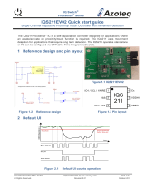
1 Reference design and pin layout
Figure 1.1 Pin Layout
Figure 1.2 IQS211AEV02
Table 1.1 Pin-out description
IQS211A in TSOT23-6
Pin
Name
Type
Function
1
IO1 / SCL / 1WIRE
Digital Input / Output
Multifunction IO1 / SCL / 1WIRE (I2C Debug Clock
signal / 1WIRE communication line)
2
VSS
Signal GND
3
IO2 / SDA
Digital Input / Output
Multifunction IO2 / SDA (I2C Debug Data output)
4
VREG
Regulator output
Requires external capacitor
5
VDDHI
Supply Input
Supply:1.8V – 3.3V
6
Cx
Sense electrode
Connect to conductive area intended for sensor
Figure 1.3 IQS211A Reference design
2 Ultra-low power configuration
For IQS211A 08000000 TSR devices (OTP Bank4: bit3 = 1 for VREG damping) the
IQS211AEV02 main board can be configured to connect IO2 to R3 = 680Ω grounding resistor.
This resistance is mandatory for the ultra-low power operational mode.
211
OUT
VSS
MOV_OUT &
RST/WAKE_IN
Cx
VDDHI
VREG
1
2
3
6
5
4
211
MOV_OUT
VSS
CONFIG_IN
Cx
VDDHI
VREG
1
2
3
6
5
4
211
OUT & MOV_PWM
VSS
RST/WAKE_IN
Cx
VDDHI
VREG
1
2
3
6
5
4
211
SCL
VSS
SDA
Cx
VDDHI
VREG
1
2
3
6
5
4
211
OUT & MOV_PWM
VSS
CONFIG_IN
Cx
VDDHI
VREG
1
2
3
6
5
4
000 -I2C
001 -Movement/Touch
010 - Movement/ Prox
011 - Movement/Input
100 - 1Wire + Mov
101 - 1Wire Short+Rdy
110 - I2C with reset indication
000 -I2C
110 -I2C with reset indication
001 -Movement/Touch (OUT)
010 - Movement/ Prox (OUT) 011 – Movement/Input
211
1Wire
VSS
MOV_OUT
Cx
VDDHI
VREG
1
2
3
6
5
4
001 -Movement/Touch (OUT)
010 - Movement/ Prox (OUT)
100 - 1Wire + Mov 101 - 1Wire Short+Rdy
211
1Wire
VSS
RDY
Cx
VDDHI
VREG
1
2
3
6
5
4
211
OUT
VSS
CONFIG_IN
Cx
VDDHI
VREG
1
2
3
6
5
4
xxx – OUT / Input
xxx – OUT&MOV / Rst&Wake xxx – OUT&MOV / Input
IQS
211A
IO1 / SCL / 1WIRE
VSS
IO2 / SDA
Cx
VDDHI
VREG
1
2
3
6
5
4
GND
C1
1uF
GND
C2
100pF
C4
100pF
C3
1uF
GND
VDDHI
GND
VREG
CX
R1
470R
IO1/SCL/DATA
IO2/SDA/EVENT
VDDHI
DS0
DS1
IO2/SDA/EVENT
IO1/SCL/DATA
GREEN
BLUE
IO2/SDA/EVENT
3
IO1/SCL/1WIRE
1
VREG
4
CX
6
GND
2
VDDHI
5
U1
IQS211A
C5
10pF
GND
R4
470R
R5
470R
VDDHI
R7
4k7
VDDHI
R6
4k7
IO1/SCL/DATA
IO2/SDA/EVENT
R2
40R

IQ Switch®
ProxSense® Series
Copyright © Azoteq (Pty) Ltd 2017
IQS211EV02 Quick start guide
Page 2 of 2
All Rights Reserved.
Revision 1.2
April 2017
Figure 2.1 IQS211A reference design (Ultra-low power)
3 Default UI
Different UI’s can be selected in the IQS211A GUI and can then be selected to run in
standalone mode.
The GUI is available for download from the Software & Tools section of azoteq.com and the
CT210 (sold separately) is used in conjunction with the GUI to select the different UI’s and
settings.
Using USBProg the IQS211A can be configured in different variations. Please note when
settings are programmed it is permanent.
GND
C1
1uF
GND
C2
100pF
C4
100pF
C3
1uF
GND
VDDHI
GND
VREG
CX
R1
470R
IO1/SCL/DATA
IO2/SDA/EVENT
VDDHI
DS1
IO1/SCL/DATA
IO2/SDA/EVENT
3
IO1/SCL/1WIRE
1
VREG
4
CX
6
GND
2
VDDHI
5
U1
IQS211A
C5
10pF
GND
R5
470R
R4
680R
IO2
GND
R4 required when
“VREG damping
on IO2” is selected
for lowest power
consumption
VDDHI
R5
10k
IO1/SCL/DATA
R2
40R
Set S1 to downward position for 1 wire communication OR
DMP (current dump) for ultra-low power consumption.
Set S1 to upward position for I2C and programming
Place a jumper pin for a halt charge / reseed input
command on IO1 (OTP option)
Place a jumper pin to connect IO2 to R3 = 680Ω resistor
for DMP option on S1
IQS211AEV02 Main PCB
/


