Broadcom Confidential ACFJ-3262-NexperiaGaN-RM100
10
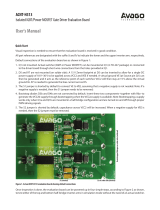
ACFJ-3262 Reference Manual Nexperia GAN039-650NBB Half-Bridge Evaluation Board
3.2 Gate Driver Circuit
The half-bridge evaluation board uses a dual-channel gate drive optocoupler U10, ACFJ-3262 to drive the GaN FETs
directly. The ACFJ-3262 is a basic gate driver optocoupler used to isolate and drive the GaN FETs. It has a rail-to-rail output
with 10A maximum output current to provide fast switching high voltage and driving current to turn-on and off the GaN
efficiently.
The ACFJ-3262 has a propagation delay of less than 95 ns. The very high CMR, common mode rejection of 100 kV/µs(min.)
is required to isolate high transient noise during the high frequency operation from causing erroneous outputs. It is certified
by UL1577 for up to VISO 5000VRMS/min and IEC 60747-5-5 for working voltage, VIORM up to 1230VPEAK.
The LED inputs of the gate driver use a split resistor network of 120Ω at the anode and cathode. This is to balance the input
impedance of the LEDs to achieve the high CMR of 100 kV/µs.
The ACFJ-3262 has a UVLO threshold voltage of 8.6V, suitable for 10V to 12V gate operation of the GaN FET
GAN039-650NBB. It has dual output, VOutP1 and VOutP2 to control the turning on and off of the GaN FET using external
15Ω gate resistors, Rgon and Rgoff. With the 12V supply, this translates to approximate 0.8A peak current to the gate of the
GaN FET.
Ferrite beads, FBL and FBH must be fitted in series with the gate of the GaN FET and should be located as close as possible
to the gate pin. Keep the gate-source loop as compact as possible to minimize the gate loop inductance. The Ferrite bead
damps the resonant circuit made up of the gate source loop inductance and the GaN FET input capacitance, thus providing
fast switching stability. Use BLM18PG300SN1D with an impedance of 30Ω at 100 MHz.
14V TVS diodes D9 and D10, can be used to clamp and protect the gate of the GaN FET and gate driver output. However,
the GaN FET does not require this diode for normal operation. The TVS diode must be selected carefully to prevent adverse
effect to the switching performance.
3.3 GaN FET Circuit
The half-bridge evaluation board uses two GaN FETs, Q1 for the high side switch and Q2 for the low side switch. The
GAN039-650NBB is a 650V, 33-mΩ normally-off GaN FET that combines Nexperia’s latest high-voltage GaN HEMT H2
technology and low-voltage silicon MOSFET technologies in a CCPAK1212 package.
Use a DC-link snubber, which consists of R17/R18/R19 and C33/C34/C35 to lower the Q factor of any resonance in the
HVDC bus. That resonance acts as a load on the high-gain amplifier, which is the GaN FET and can lead to instability. The
remaining capacitors, C4-6/C17/C24.C36–16 are high-frequency DC-link components, placed very close to the GaN FETs
for fast switching half-bridge operations.