
User Guide
Broadcom ACNT-H343-UG101
March 11, 2019
Application Circuit Description
The Broadcom
®
ACNT-H343 is an isolated gate driver that
provides 5A of output current in 15-mm/14.2-mm creepage
and clearance package. The voltage and high peak output
current supplied by this optocoupler make it ideally suited to
direct-drive the IGBT with ratings up to 1700V/120A. It is
also designed to drive different sizes of buffer stage that will
make the class of IGBT scalable. This ACNT-H343 device
provides a single isolation solution suitable for both low and
high power ratings of motor control and inverter applications
with working voltage as high as 2262 Vpk.
Quick Start
Visual inspect the ACNT-H343 evaluation board to make
sure it has been received in good condition.
The ACNT-H343 (IC1) is a 5A gate driver optocoupler
suitable for driving 1700V, 120A IGBT or power MOSFET
used in either power converters or motor drives. The
evaluation board can be used as a reference design to
provide necessary interface details between a PWM
controller and an IGBT/Power MOSFET. The ACNT-H343 is
a single-channel driver. For a dual-channel driver
configured in a totem-pole arrangement, stack two
evaluation board, one on top the other.
NOTE: The PCB used for this evaluation board is a
four-layer PCB, which is required to minimize the
output noise due to the 5A high output current at
50-kHz PWM switching signal.
Confirm that the default connections of the evaluation board
are as follows (see Figure 1):
1. R2 is not mounted. R2 (usually set to carry less than
10 percent of the LED current) can be mounted if
regulating the LED forward voltage V
F
is required (V
F
varies if the temperature drifts) when the input voltage
across CON1 pins is fixed.
2. J1 is not shorted by default. This J1 link, will short the V
E
and V
SS
terminals together if negative supply is not
needed. V
E
is also connected to the emitter/source
terminal of the IGBT/power MOSFET inside the board.
3. Q1 is not mounted by default. A suitable IGBT/power
MOSFET can be mounted here.
4. The CON1 connector allows for the connection of the
PWM input signal with Vpp of 5V.
5. The CON2 connector allows for the connection of
positive (across V
DD
and V
E
) and negative (across V
SS
and V
E
) supplies.
6. TP1 and TP2 test points monitor the output voltages at
pin-7 of the IC1 and the gate of Q1, respectively.
7. Two M3 holes allow for the evaluation board to be
mounted on external platform, such as a chassis.
ACNT-H343
5A Gate Drive Optocoupler Evaluation Board

Broadcom ACNT-H343-UG101
2
ACNT-H343 User Guide 5A Gate Drive Optocoupler Evaluation Board
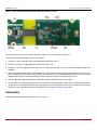
Figure 1: Actual ACNT-H343 Evaluation Board Showing Default Connections
No component is mounted on the solder side (bottom layer), so it is not shown in the figures.
To power up the evaluation board, perform these steps:
1. Connect a 1700V, 120A IGBT (with gate capacitance about 25 nF) at Q1.
2. Connect a 50 kHz +5V PWM signal with a 50 percent duty cycle
3. Connect a +15V DC supply across V
DD
and V
SS
. For verification purposes, short V
E
to V
SS
if the negative supply is not
available.
4. When the preceding steps have been performed, you can observe the output drive signal behavior at TP1 point, TP2
point, or both points. If the proper 1700V, 120A is not available yet, you can simulate the performance of the gate driving
signals of the board by connecting an external 25-nF capacitor across the G and E terminals of Q1.
5. The following sections describe how the evaluation board can be powered up in more detail.
6. You can stack two evaluation boards (from top to bottom) to form a half-bridge inverter arm by soldering S3 and S4 of
the top arm to S1 and S2 of the bottom arm, respectively. You can do this action if the HV bus voltage is not more than
1700V. For more information about this configuration, see Half-Bridge Inverter Configuration.
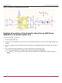
Schematics
Schematics of the evaluation board are as shown in Figure 2.
IC1
R2 J1 Q1 CON1 CON2
M3
M3
s1
s2
s3
s4
TP1 TP2

Broadcom ACNT-H343-UG101
3
ACNT-H343 User Guide 5A Gate Drive Optocoupler Evaluation Board
Figure 2: Schematics of the ACNT-H343 Evaluation Board
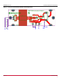
Practical Connections of the Evaluation Board Using IGBT/Power
MOSFET for an Actual Inverter Test
For connection details, see Figure 3.
1. Solder an actual IGBT at Q1.
2. Connect a +15V DC supply across V
DD
and V
SS
. For verification purposes, short V
E
to V
SS
if the negative supply is not
available.
3. C
onnect the signal output (up to 50 kHz) from the microcontroller to the PWM 5V signal input across pin IN1+ and IN1- of
CON1.
4. Use a multi-channel digital oscilloscope to monitor the waveforms at the following points:
a. The LED signal across the IN1+ and IN1- pins, which represents the input PWM signal.
b. V
OUT
across V
O
(TP1) and V
E
terminals, which is the output signal from the ACNT-H343 (a differential probe is
needed).

Broadcom ACNT-H343-UG101
4
ACNT-H343 User Guide 5A Gate Drive Optocoupler Evaluation Board
Figure 3: Connection of the Evaluation Board in Actual Applications
IN1+
IN1-
50kHz 5V PWM i/p Signal
COM
+15V
1700V 120A
IGBT


Broadcom ACNT-H343-UG101
6
ACNT-H343 User Guide 5A Gate Drive Optocoupler Evaluation Board
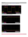
ATTENTION: Figure 6 shows the corresponding IN+ and Vo signals when J1 link is removed and A –5V supply is connected
to V
SS
terminal at CON2.
Figure 6: IN+ and Vo (TP1) Signals after Removing a J1 Short
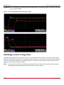
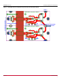
Half-Bridge Inverter Configuration
The ACNT-H343 evaluation board, as shown in Figure 1, accommodates an ACNT-H343 IC. Therefore, to drive top and
bottom arms of the half-bridge inverter, two evaluation boards are required. You can stack the two boards together as shown
in Figure 7 (with proper connections). This stacking allows you to easily test the performance of gate driver in an actual
application under real-life operating conditions.
NOTE: As can be seen on the board, the isolation circuitry (at the far left) is easily contained within a small area while
maintaining adequate spacing for good voltage isolation and easy assembly.

Broadcom ACNT-H343-UG101
7
ACNT-H343 User Guide 5A Gate Drive Optocoupler Evaluation Board
Figure 7: Half-Bridge Inverter Configuration by Connecting Two Evaluation Boards
g
IN1+
IN1-
IN2+
IN2 -
HVBus +
HVBus -
Soldering Connection
Soldering Connection
Connection
to load
-5V
PS1b
15 V
PS1a
-5V
PS2b
15 V
PS2a
From Microcontroller

Broadcom, the pulse logo, Connecting everything, Avago Technologies, Avago, and the A logo are among the trademarks
of Broadcom and/or its affiliates in the United States, certain other countries, and/or the EU.
Copyright © 2019 Broadcom. All Rights Reserved.
The term “Broadcom” refers to Broadcom Inc. and/or its subsidiaries. For more information, please visit www.broadcom.com.
Broadcom reserves the right to make changes without further notice to any products or data herein to improve reliability,
function, or design. Information furnished by Broadcom is believed to be accurate and reliable. However, Broadcom does
not assume any liability arising out of the application or use of this information, nor the application or use of any product or
circuit described herein, neither does it convey any license under its patent rights nor the rights of others.
-
 1
1
-
 2
2
-
 3
3
-
 4
4
-
 5
5
-
 6
6
-
 7
7
-
 8
8


Ask a question and I''ll find the answer in the document
Finding information in a document is now easier with AI
Related papers
-
Broadcom ACNU-3430 User guide
-
-
-
 Avago ACNT-H313, Isolated IGBT/Power MOSFET Gate Driver Evaluation Board - User's User manual
-
Broadcom ACFJ-3262 User guide
-
-
-
-
-

Other documents
-
Superlux PS2A User guide
-
Tote Vision Computer Monitor LCD-1700V User manual
-
Copystar CS-4035 User manual
-
Texas Instruments OPA2835DGS, OPA2836DGS EVM User guide
-
Sanyo SC-L180H User manual
-
-
 Avago ACPL-P349 User manual
-
-
Infineon EVAL3K3WTPPFCSICTOBO1 Operating instructions
-
