Page is loading ...

VC ADSR V2.0.3 - ASSEMBLY GUIDE – Rev. Feb 2022
THANKS FOR CHOOSING ONE OF OUR KITS!
This manual has been written taking into account the common issues that we often find people experience in our
workshops. The order in which the components are placed on the board is meant to make assembly as easy as possible.
Some steps are not obvious, so even if you're an experienced DIYer please read the steps thoroughly before starting. You
will be soldering both boards at the same time.
If this is your first project, please read this article before you start assembling the kit:
www.befaco.org/howto/
GOOD LUCK!
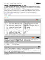
RESISTORS
It’s strongly recommended to measure the resistors with a multimeter. Color code might be hard to read with blue/green
background.
Qty
Value
Code
Name on PCB
19
100k
Brown, black, black, orange, brown
R4, R8, R9, R12, R13, R18, R102 R113, R114, R115, R116, R118,
R119, R121, R122, R125, R126, R128, R129
9
1k
Brown, black, black, brown, brown
R1, R21, R100, R101, R117, R120, R123, R124, R127
5
10k
Brown, black, black, red, brown
R10, R16, R19, R22, R104
4
2k2
Red, red, black, brown, brown
R3, R7, R20, R107
4
4K7
Yellow, violet, black, brown, brown
R2, R11, R17, R105
3
47k
Yellow, violet, black, red, brown
R106, R108, R112
3
3M
Orange, black, black, yellow, brown
R109, R110, R111
2
56k
Green, blue, black, red, brown
R15, R103
1
3k3
Orange, orange, black, brown, brown
R14
1
330k
Orange, orange, black, orange, brown
R5
1
1M
Brown, black, black, yellow, brown
R6
DIODES
Solder the diodes observing their polarity. The black or white line on the diode must match with the white line on the
diode symbol on the PCB silkscreen.
Qty
Value
Name on PCB
5
1N4148 (orange color)
D1, D2, D3, D4, D100
2
1N5817 (black color)
D5, D6
FERRITES
Solder the two ferrite beads by using a recycled resistor leg passed through each ferrite and proceed as if it were a
resistor. Ferrite beads don't have polarity.
Qty
Name on PCB
2
FER_1, FER_2
1

VC ADSR V2.0.3 - ASSEMBLY GUIDE – Rev. Feb 2022
ICs
First place the sockets (taking care to orientate them properly – the notch or dot on one end of the IC
should match the image on the silkscreen) and solder them into their correct positions.
Qty
Value
Name on PCB
1
DIP16
CD4052
4
DIP14
CD4073, CD4013, TL074/84, TL074/84
1
DIP8
TL072/82
CAPACITORS
Identifying capacitors can be quite tricky. Codes stated are indicative, please take a look at this guide for help identifying
capacitors: http://www.wikihow.com/Read-a-Capacitor
Qty
Value
Code
Name on PCB
13
100n
104
C1, C2, C4, C8, C9, C10, C11, C13, C14, C16, C17, C100, C101
2
1n
102
C7, C12
1
100p
101/100
C5
1
10n
10nK
C3
1
470n
.47 (or 473)
C15
1
2n2
2200 (red color)
C6
TRANSISTORS
Be sure they are orientated correctly. The curved and flat sides of the silkscreen outline of the transistor on the PCB must
match that of the transistor’s body.
Qty
Value
Name on PCB
4
2N3904
T2, T3, T5, T6
3
2N3906
T1, T4, T100
REGULATOR
Make sure the voltage regulator is positioned correctly with reference to the silkscreen outline on the PCB
Qty
Code
Name on PCB
1
78L05
IC2
ELECTROLYTIC CAPACITORS
Values are written on the side of the capacitor. Mind their polarity (The long leg of the capacitor is the positive (+)).
Qty
Value
Code
Name on PCB
2
10uf
10uf
C18, C19
2

VC ADSR V2.0.3 - ASSEMBLY GUIDE – Rev. Feb 2022
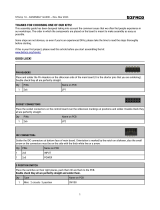
THIS IS A GOOD MOMENT TO SPLIT THE BOARDS APART.
SOCKET CONNECTORS
Place the socket connectors over the silkscreen markings at positions “TO_CON_1” & “TO_CON_2” on the
control board and solder. Double check they all are perfectly straight.
PIN HEADERS
Place and solder the pin headers at “CON_1” & “CON_2” on the main board, where the silkscreen indicates
(it is the shorter pins that you are soldering).Double check they all are perfectly straight.
POWER CONNECTOR
Solder the power connector at “POWER1”, ensuring it is facing out from the edge of the PCB. The small
arrow on the connectors must be on the side with the thick white line.
SPACERS
Secure the spacers onto Control PCB (through the holes with silver outlines) with the main body of the
spacer on the component side, and the nut on the opposite.
FADERS
Solder the faders on the PCB where it is indicated by the silkscreen.
Qty
Name on PCB
4
A_POT, D_POT, R_POT, S_POT
MECHANICAL COMPONENTS MOUNTING TIPS:
Now we will proceed to mount the jacks, potentiometer, switches and LEDs. This part of the assembly is
CRITICAL. Please take your time and read the following instructions carefully.
These components must NOT be soldered until they are placed on the PCB and fully attached to the front
panel.
There are two reasons for this:
The height of the panel components are not all the same. Because of this, if not attached properly
before soldering, they will not stay properly seated against the panel. This might cause mechanical
stress reducing their life expectancy and in the worst case cause them to break.
The second reason is that it is very difficult to align the components to the holes if the panel is not
positioned prior to soldering. In the case of the LEDs, they are almost impossible to set to the correct
height without reference to the front panel.
3

VC ADSR V2.0.3 - ASSEMBLY GUIDE – Rev. Feb 2022
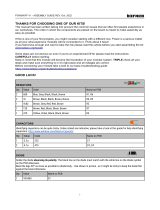
LEDs
Place the LEDs onto the PCB minding, their polarity, but don't solder them until the front panel is in place. This is the only
way to solder them in the right position.
The long leg is the positive and the short the negative. On the PCB the square pad indicates the negative side and there
is a + symbol to indicate the positive.
Qty
Name on PCB
5
L_0, L_A, L_D, L_R, L_S
POTENTIOMETER
Now place the potentiometer on the PCB. Do not place them all the way down, leave them loose and... don't solder them
yet!
Qty
Type
Name on PCB
1
Dual (6pin) B100K
SHAPE
TOGGLE SWITCH
Remove the two nuts and the tabbed washer from the toggle switches (if they are still on the switch). Discard one nut
and the tabbed washer, but keep one nut for securing to the front panel later. Place the toggle switches on the PCB but
don't solder them yet.
Qty
Type
Name on PCB
1
SPDT ON-ON Toggle
MODE
PUSH BUTTON
Remove the nut and the washer from the push button. Throw the washer away, it will not be used. Now fit the push button
onto the PCB but again...don’t solder it yet.
Qty
Type
Name on PCB
1
Red Cap OFF/ON Push-Button
M_TRIG
MINI-JACKS
Place all the mini-jacks onto the PCB ensuring they are on the silkscreen side, but don't solder yet.
Note: The two rows of 4x mini-jacks at the bottom of the control PCB will be orientated such that they face each other
with each opposite pair of mini-jacks sharing a solder point for their 3rd (outer) legs.
Caution: the switch nut and the jack nuts look the same, but they are not equally sized and will not fit in each others'
thread, so make sure to keep them separate!
4

VC ADSR V2.0.3 - ASSEMBLY GUIDE – Rev. Feb 2022
ICs
Next place the ICs in their respective sockets (again taking note of their orientation – the notch or dot on the top of the
IC must match that of the socket and silkscreen).
Qty
Value
Name on PCB
2
TL074
TL074/84, TL074/84
1
CD4013
CD4013
1
CD4052
CD4052
1
CD4073
CD4073
1
TL072
TL072/82
FRONT PANEL
Attach the front panel adjusting the parts one by one if necessary until they fit. At this point a pair of fine tweezers can
be helpful.
To finish:
- Secure the parts to the panel in this order: A) Mini-jacks B) Switch C) Pot D) Push button.
- Ensuring all of the above parts are flush with the panel then you can finally solder them!
- Next, adjust the LEDs so that they are flush with the panel and solder them.
- Connect the main PCB to the control PCB using the pin headers and by threading the M3 screws through the main
PCB and securing them to the spacers. The main PCB should be orientated so that the component side is facing towards
the front panel.
- Put the knob on the potentiometer and the red end-caps on the switches/faders.
- Connect the power ribbon cable: The red wire (-12V) on the power ribbon cable corresponds to pin number one on
the male power connector. The number one pin is indicated with a small triangle on the male power connector and a
white line on the main PCB. A white or black line (or “-12v”) marked on your power bus normally indicates the
corresponding pin.
ENJOY YOUR NEW BEFACO MODULE!
5

VC ADSR V2.0.3 - ASSEMBLY GUIDE – Rev. Feb 2022
6
/


