Page is loading ...

EVEN_VCO V0.3.3 - ASSEMBLY GUIDE – Rev. Oct 2022
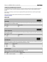
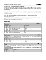
THANKS FOR CHOOSING ONE OF OUR KITS!
This manual has been written taking into account the common issues that we often find people experience in our
workshops. The order in which the components are placed on the board is meant to make assembly as easy as possible.
Some steps are not obvious, so even if you're an experienced DIYer please read the steps thoroughly before starting.
If this is your first project, please read this article before you start assembling the kit:
www.befaco.org/howto/
You will be soldering both boards at the same time. Please refer to page 7 for a component placing reference. Some
names could be small and difficult to spot.
RESISTORS
Color code can be difficult to identify, we strongly recommend to use a multimeter.
Qty
Value
Code
Name on PCB
13
100k
Brown, Black, Black, Orange, Brown
R16, R17, R18, R20, R22, R25, R27 (close to IC6), R30, R36, R45,
R108, R111, R112
9
10k
Brown, Black, Black, Red, Brown
R11 (close to D5), R31, R33, R35, R37, R38, R40, R120, R124
7
1K
Brown, Black, Black, Brown, Brown
R5, R41, R43, R101, R103, R104, R105
4
22k
Red, Red, Black, Red, Brown
R12, R15, R24, R44
2
1.5k
Brown, Green, Black, Brown, Brown
R9, R10 (close to T2)
2
3.3k
Orange, Orange, Black, Brown Brown
R100, R102
2
43k
Yellow, Orange, Black, Red, Brown
R29, R32
2
47k
Yellow, Purple, Black, Red, Brown
R21, R107
2
220k
Red, Red, Black, Orange, Brown
R23, R42
1
4Ω22
Yellow, red, red, silver, brown
R3 (place this resistor standing in order to fit in the PCB silkscreen)
1
270Ω
Red, Purple, Black, Black, Brown
R7
1
390Ω
Orange, White, Black, Black, Brown
R34
1
510Ω
Green, brown, black, black, brown
R4
1
2.2k
Red, Red, Black, Brown, Brown
R14
1
6k2
Blue, red, black, brown, brown
R1,
1
12k
Brown, Red, Black, Red, Brown
R106
1
20k
Red, Black, Black, Red, Brown
R28
1
36k
Orange, Blue, Black, Red, Brown
R109
1
82k
Grey, Red, Black, Red, Brown
R39
1
95k3
White, green, orange, red, brown
R6
1
130k
Brown, Orange, Black Orange, Brown
R114
1
150k
Brown, Green, Black, Orange, Brown
R8
1
200k
Red, Black, Black, Orange, Brown
R46
1
330k
Orange, Orange, Black, Orange, Brown
R13
1
430k
Yellow, Orange, Black, Orange, Brown
R26
1
820k
Gray, red, black, orange, brown
R2
1
2M
Red, Black, Black, Yellow, Brown
R19
1
50K 0.1%
Brown background “DALE 5002B”
R121
2
100K 0.1%
Brown background “DALE 1003B”
R110, R113
R115 – This resistor is no longer used so we must bridge the solder points with the leg of a resistor or wire.
1

EVEN_VCO V0.3.3 - ASSEMBLY GUIDE – Rev. Oct 2022
DIODES
Solder the diodes observing their polarity. The black or white line on the diode must match with the white line on the
diode symbol on the PCB silkscreen.
Qty
Value
Name on PCB
6
1N4148 (Orange)
D1, D2, D3, D4, D5, D8
2
1N5817 (Black)
D6, D7
2
BZX550 4V7
D100, D101
FERRITE
Solder the two ferrite beads by using a recycled resistor leg passed through each ferrite and proceed as if it were a
resistor. Ferrite beads don't have polarity.
Qty
Name on PCB
2
FERRITE+, FERRITE-
ICs
First place the sockets (taking care to orientate them properly – the notch or dot on one end of the IC should match the
image on the silkscreen) and solder them into their correct positions.
Next place the ICs in their respective sockets (again taking note of their orientation – the notch or dot on the top of the
IC must match that of the socket and silkscreen).
Qty
Value
Name on PCB
1
LM393
IC4
3
TL072
IC5, IC6, IC7
2
LF412
IC2, IC3
CAPACITORS
Identifying capacitors can be quite tricky. Codes stated are indicative, please take a look at this guide for help identifying
capacitors: http://www.wikihow.com/Read-a-Capacitor.
Qty
Value
Code
Name on PCB
C22 is no longer needed
12
100n
104
C2, C4, C5, C8, C10, C15, C17, C19, C20, C23, C25, C100
4
1n
102
C1, C3, C12, C101
3
10p
10
C13, C18, C26
2
680n
.68K63
C11, C24
2
47p
47
C6, C9
1
2.2n
2n2k100
C21
1
2.2n
2200 (red)
C7 (WIMA)
2

EVEN_VCO V0.3.3 - ASSEMBLY GUIDE – Rev. Oct 2022
ELECTROLYTIC CAPACITORS
Values are written on the side of the capacitor. Mind their polarity (The long leg of the capacitor is the positive (+)).
Qty
Value
Code
Name on PCB
2
10µF
10µF
C14, C16
TRANSISTORS
Be sure they are orientated correctly. The curved and flat sides of the silkscreen outline of the transistor
on the PCB must match that of the transistor’s body.
Qty
Value
Name on PCB
3
2n3904
T1, T3, T4
1
2n3906
T2
1
LM336
IC1
TRIMMERS
Solder the trimmers onto the PCB where the silkscreen indicates, with the screw facing out from the edge of the PCB.
Doublecheck trimmer values before sodlering!!
Qty
Value
Code
Name on PCB
3
10k
X 103
REF_ADJ, WIDTH (identifying text on opposite side of PCB), INIT
1
1k
X 102
V/OCT_LIN
SOCKET CONNECTORS
Place and solder the socket connectors on the control board at positions “TO_MAIN_A” & “T0_MAIN_B” . Double check
they all are perfectly straight.
PIN HEADERS
Place and solder the Pin Headers on the Main Board at “MAIN_A100” & “MAIN_B100” (it is the shorter pins that you are
soldering). Double check they all are perfectly straight.
POWER CONNECTOR
Solder the power connector at “POWER”, ensuring it is facing out from the edge of the PCB. The small arrow on the
connectors must be on the side with the thick white line.
3

EVEN_VCO V0.3.3 - ASSEMBLY GUIDE – Rev. Oct 2022
SPACERS
Secure the spacers onto the CONTROL PCB (through the two holes with silver outlines) with the main body of the spacer
on the component side, and the nut on the opposite.
FRONT PANEL COMPONENTS MOUNTING TIPS:
Now we will proceed to mount mechanical components. This part of the assembly is CRITICAL. Please take your time and
read the following instructions carefully.
These components must NOT be soldered until they are placed on the PCB and fully attached to the front panel.
There are two reasons for this:
The height of the panel components are not all the same. Because of this, if not attached properly before
soldering, they will not stay properly seated against the panel. This might cause mechanical stress reducing their
life expectancy and in the worst case cause them to break.
The second reason is that it is very difficult to align the components to the holes if the panel is not positioned
prior to soldering.
MINI-JACKS
Place all the mini-jacks onto the PCB ensuring they are on the silkscreen side, but don't solder yet.
POTENTIOMETERS
Place the potentiometers, making sure they do not go all the way down. They need to be flat against the panel. Do not
solder them yet!
Qty
Type
Name on PCB
2
Single (3pin)
FINE_TUNE, PW
ROTARY SWITCH
Cut and remove the locating lug. Place and solder the rotary switch “OCTAVE_SELECTOR” on the silkscreen side of the
PCB.
Once soldered, also cut the long central leg so it won't touch components on the other PCB.
Qty
Type
Name on PCB
1
Rotary Switch
OCTAVE_SELECTOR
4

EVEN_VCO V0.3.3 - ASSEMBLY GUIDE – Rev. Oct 2022
FRONT PANEL
Attach the front panel adjusting the parts one by one if necessary until they fit. At this point a pair of fine tweezers can
be helpful.
To finish:
- Screw in the parts in this order: A) Mini-jacks B) Pots
- Ensuring all of the above parts are flush with the panel then you can finally solder them!
- Connect the main PCB to the control PCB using the pin headers and by threading the M3 screws through the main
PCB and securing them to the spacers. The main PCB should be orientated so that the component side is facing
towards the front panel.
- Put the knobs on the potentiometers.
- Connect the power ribbon cable: The red wire (-12V) on the power ribbon cable corresponds to pin number one
on the male power connector. The number one pin is indicated with a small triangle on the male power connector and a
white line on the main PCB. A white or black line (or “-12v”) marked on your power bus normally indicates the
corresponding pin.
CALIBRATION
The tuning process is an iteration of successive approximations. We will try in each iteration to get closer to a perfect
tune.
First step will be to get TP_1 (located in control Board) to measure 1.5v using REF trimmer.
With the INIT trimmer and the TUNE potentiometer we will adjust the relationship between the actual pitch and the
values written in the front panel. If during the process the TUNE potentiometer is not enough, use the INIT trimmer to
bring the whole scale up/down.
With the WIDTH trimmer we will adjust the relationship between the actual pitch and the input voltage. Then, with the
V/OCT_LIN trimmer we will adjust the curve at the end of it's range is needed.
Follow the flow diagram on the next page to help you calibrate the EvenVCO:
5

EVEN_VCO V0.3.3 - ASSEMBLY GUIDE – Rev. Oct 2022
6

EVEN_VCO V0.3.3 - ASSEMBLY GUIDE – Rev. Oct 2022
7

EVEN_VCO V0.3.3 - ASSEMBLY GUIDE – Rev. Oct 2022
8
/


