
Preliminary User’s Manual
µ
µµ
µ
PD98502
Network Controller
Document No. S15543EJ1V0UM00 (1st edition)
Date Published December 2001 NS CP(K)
2001
Printed in Japan

Preliminary User’s Manual S15543EJ1V0UM
2
[MEMO]

Preliminary User’s Manual S15543EJ1V0UM
3
SUMMARY OF CONTENTS
CHAPTER 1 INTRODUCTION .................................................................................................................. 23
CHAPTER 2 V
R
4120A ............................................................................................................................... 57
CHAPTER 3 SYSTEM CONTROLLER ................................................................................................... 185
CHAPTER 4 ATM CELL PROCESSOR .................................................................................................. 229
CHAPTER 5 ETHERNET CONTROLLER............................................................................................... 277
CHAPTER 6 USB CONTROLLER .......................................................................................................... 309
CHAPTER 7 PCI CONTROLLER ............................................................................................................ 370
CHAPTER 8 UART .................................................................................................................................. 414
CHAPTER 9 TIMER ................................................................................................................................. 424
CHAPTER 10 MICRO WIRE.................................................................................................................... 427
APPENDIX A MIPS III INSTRUCTION SET DETAILS............................................................................ 431
APPENDIX B V
R
4120A COPROCESSOR 0 HAZARDS......................................................................... 590

Preliminary User’s Manual S15543EJ1V0UM
4
NOTES FOR CMOS DEVICES
1 PRECAUTION AGAINST ESD FOR SEMICONDUCTORS
Note:
Strong electric field, when exposed to a MOS device, can cause destruction of the gate oxide and
ultimately degrade the device operation. Steps must be taken to stop generation of static electricity
as much as possible, and quickly dissipate it once, when it has occurred. Environmental control
must be adequate. When it is dry, humidifier should be used. It is recommended to avoid using
insulators that easily build static electricity. Semiconductor devices must be stored and transported
in an anti-static container, static shielding bag or conductive material. All test and measurement
tools including work bench and floor should be grounded. The operator should be grounded using
wrist strap. Semiconductor devices must not be touched with bare hands. Similar precautions need
to be taken for PW boards with semiconductor devices on it.
2 HANDLING OF UNUSED INPUT PINS FOR CMOS
Note:
No connection for CMOS device inputs can be cause of malfunction. If no connection is provided
to the input pins, it is possible that an internal input level may be generated due to noise, etc., hence
causing malfunction. CMOS devices behave differently than Bipolar or NMOS devices. Input levels
of CMOS devices must be fixed high or low by using a pull-up or pull-down circuitry. Each unused
pin should be connected to V
DD
or GND with a resistor, if it is considered to have a possibility of
being an output pin. All handling related to the unused pins must be judged device by device and
related specifications governing the devices.
3 STATUS BEFORE INITIALIZATION OF MOS DEVICES
Note:
Power-on does not necessarily define initial status of MOS device. Production process of MOS
does not define the initial operation status of the device. Immediately after the power source is
turned ON, the devices with reset function have not yet been initialized. Hence, power-on does
not guarantee out-pin levels, I/O settings or contents of registers. Device is not initialized until the
reset signal is received. Reset operation must be executed immediately after power-on for devices
having reset function.

Preliminary User’s Manual S15543EJ1V0UM
5
VR4100, VR4102, VR4111, VR4120A, VR4300, VR4305, VR4310, VR4400, VR5000, VR10000, VR Series, VR4000
Series, V
R4100 Series, and EEPROM are trademarks of NEC Corporation.
Micro Wire is a trademark of National Semiconductor Corp.
iAPX is a trademark of Intel Corp.
DEC VAX is a trademark of Digital Equipment Corp.
UNIX is a registered trademark in the United States and other countries, licensed exclusively through
X/Open Company, Ltd.
Ethernet is a trademark of Xerox Corp.
MIPS is a trademark of MIPS Technologies, Inc.
• The information contained in this document is being issued in advance of the production cycle for the
device. The parameters for the device may change before final production or NEC Corporation, at its own
discretion, may withdraw the device prior to its production.
• Not all devices/types available in every country. Please check with local NEC representative for availability
and additional information.
• No part of this document may be copied or reproduced in any form or by any means without the prior written
consent of NEC Corporation. NEC Corporation assumes no responsibility for any errors which may appear in
this document.
• NEC Corporation does not assume any liability for infringement of patents, copyrights or other intellectual property
rights of third parties by or arising from use of a device described herein or any other liability arising from use
of such device. No license, either express, implied or otherwise, is granted under any patents, copyrights or other
intellectual property rights of NEC Corporation or others.
• Descriptions of circuits, software, and other related information in this document are provided for illustrative
purposes in semiconductor product operation and application examples. The incorporation of these circuits,
software, and information in the design of the customer's equipment shall be done under the full responsibility
of the customer. NEC Corporation assumes no responsibility for any losses incurred by the customer or third
parties arising from the use of these circuits, software, and information.
• While NEC Corporation has been making continuous effort to enhance the reliability of its semiconductor devices,
the possibility of defects cannot be eliminated entirely. To minimize risks of damage or injury to persons or
property arising from a defect in an NEC semiconductor device, customers must incorporate sufficient safety
measures in its design, such as redundancy, fire-containment, and anti-failure features.
• NEC devices are classified into the following three quality grades:
"Standard", "Special", and "Specific". The Specific quality grade applies only to devices developed based on a
customer designated "quality assurance program" for a specific application. The recommended applications of
a device depend on its quality grade, as indicated below. Customers must check the quality grade of each device
before using it in a particular application.
Standard: Computers, office equipment, communications equipment, test and measurement equipment,
audio and visual equipment, home electronic appliances, machine tools, personal electronic
equipment and industrial robots
Special: Transportation equipment (automobiles, trains, ships, etc.), traffic control systems, anti-disaster
systems, anti-crime systems, safety equipment and medical equipment (not specifically designed
for life support)
Specific: Aircraft, aerospace equipment, submersible repeaters, nuclear reactor control systems, life
support systems or medical equipment for life support, etc.
The quality grade of NEC devices is "Standard" unless otherwise specified in NEC's Data Sheets or Data Books.
If customers intend to use NEC devices for applications other than those specified for Standard quality grade,
they should contact an NEC sales representative in advance.
M5D 98. 12

6
Preliminary User’s Manual S15543EJ1V0UM
PREFACE
Readers This manual is intended for engineers who need to be familiar with the capability of
the
µ
PD98502 in order to develop application systems based on it.
Purpose The purpose of this manual is to help users understand the hardware capabilities
(listed below) of the
µ
PD98502.
Configuration This manual consists of the following chapters:
• Introduction
• VR
4120A CPU
• System controller
• ATM cell processor
• Ethernet controller
• USB controller
• PCI controller
• UART
• Timer
• Micro Wire
Guidance Readers of this manual should already have a general knowledge of electronics, logic
circuits, and microcomputers.
To gain an overall understanding of the function of the
µ
PD98502:
→ Read through all the chapters, in sequence.
To check the electrical characteristics of the
µ
PD98502:
→ Refer to the separate data sheet.
Notation This manual uses the following conventions:
Data bit significance: High-order bits on the left side;
low-order bits on the right side
Active low: XXXX_B (Pin and signal names are suffixed with _B.)
Note: Explanation of an indicated part of text
Caution: Information requiring the user’s special attention
Remark: Supplementary information
Numerical value: Binary ... xxxx or xxxxB
Decimal ... xxxx
Hexadecimal ... xxxxH
Related Document Use this manual in combination with the following document.
The related documents indicated in this publication may include preliminary versions.
However, preliminary versions are not marked as such.
•
µ
PD98502 Data Sheet: S15409E

Preliminary User’s Manual S15543EJ1V0UM
7
CONTENTS
CHAPTER 1 INTRODUCTION ............................................................................................................... 23
1.1 Features ...................................................................................................................................... 23
1.2 Ordering Information................................................................................................................. 23
1.3 System Configuration................................................................................................................ 24
1.4 Block Diagram (Summary)........................................................................................................ 25
1.5 Block Diagram (Detail)............................................................................................................... 26
1.5.1 V
R
4120A RISC processor core......................................................................................................26
1.5.2 IBUS ..............................................................................................................................................27
1.5.3 System controller...........................................................................................................................28
1.5.4 ATM cell processor........................................................................................................................29
1.5.5 Ethernet controller .........................................................................................................................30
1.5.6 USB controller ...............................................................................................................................31
1.5.7 PCI controller.................................................................................................................................32
1.6 Pin Configuration (Bottom View) .............................................................................................33
1.7 Pin Function ...............................................................................................................................37
1.7.1 Power supply .................................................................................................................................37
1.7.2 System PLL power supply .............................................................................................................37
1.7.3 USB PLL power supply..................................................................................................................37
1.7.4 System control interface ................................................................................................................38
1.7.5 Memory interface...........................................................................................................................39
1.7.6 PCI interface..................................................................................................................................41
1.7.7 ATM interface ................................................................................................................................43
1.7.8 Ethernet interface ..........................................................................................................................45
1.7.9 USB interface ................................................................................................................................46
1.7.10 UART interface ..............................................................................................................................47
1.7.11 Micro Wire interface.......................................................................................................................47
1.7.12 Parallel port interface.....................................................................................................................47
1.7.13 Boundary scan interface................................................................................................................47
1.7.14 I.C. – open .....................................................................................................................................48
1.7.15 I.C.– pull down...............................................................................................................................48
1.7.16 I.C. – pull down with resistor..........................................................................................................48
1.7.17 I.C. – pull up ..................................................................................................................................48
1.8 I/O Register Map......................................................................................................................... 49
1.9 Memory Map ............................................................................................................................... 53
1.10 Reset Configuration................................................................................................................... 54
1.11 Interrupts .................................................................................................................................... 55
1.12 Clock Control Unit ..................................................................................................................... 56
CHAPTER 2 V
R
4120A ............................................................................................................................ 57
2.1 Overview for V
R
4120A ............................................................................................................... 57
2.1.1 Internal block configuration............................................................................................................58
2.1.2 VR
4120A registers .........................................................................................................................59
2.1.3 V
R
4120A instruction set overview..................................................................................................60
2.1.4 Data formats and addressing.........................................................................................................61
2.1.5 Coprocessors (CP0) ......................................................................................................................63

8
Preliminary User’s Manual S15543EJ1V0UM
2.1.6 Floating-point unit (FPU)................................................................................................................64
2.1.7 CPU core memory management system (MMU) ...........................................................................65
2.1.8 Translation lookaside buffer (TLB).................................................................................................65
2.1.9 Operating modes ...........................................................................................................................65
2.1.10 Cache ............................................................................................................................................65
2.1.11 Instruction pipeline.........................................................................................................................66
2.2 MIPS III Instruction Set Summary.............................................................................................66
2.2.1 MIPS III ISA instruction formats .....................................................................................................66
2.2.2 Instruction classes .........................................................................................................................67
2.3 Pipeline........................................................................................................................................84
2.3.1 Pipeline stages ..............................................................................................................................84
2.3.2 Branch delay..................................................................................................................................87
2.3.3 Load delay .....................................................................................................................................87
2.3.4 Pipeline operation ..........................................................................................................................88
2.3.5 Interlock and exception handling ...................................................................................................94
2.3.6 Program compatibility ..................................................................................................................100
2.4 Memory Management System ................................................................................................101
2.1.1 Translation lookaside buffer (TLB)..............................................................................................101
2.1.2 Virtual address space ..................................................................................................................102
2.1.3 Physical address space ...............................................................................................................116
2.1.4 System control coprocessor.........................................................................................................117
2.1.5 CP0 registers ...............................................................................................................................119
2.5 Exception Processing.............................................................................................................129
2.5.1 Exception processing operation...................................................................................................129
2.5.2 Precision of exceptions................................................................................................................130
2.5.3 Exception processing registers ....................................................................................................130
2.1.4 Details of exceptions....................................................................................................................142
2.1.5 Exception processing and servicing flowcharts............................................................................158
2.2 Initialization Interface ..............................................................................................................165
2.2.1 Cold reset ....................................................................................................................................165
2.2.2 Soft reset .....................................................................................................................................165
2.2.3 V
R
4120A processor modes..........................................................................................................165
2.3 Cache Memory..........................................................................................................................168
2.3.1 Memory organization ...................................................................................................................168
2.3.2 Cache organization......................................................................................................................169
2.3.3 Cache operations.........................................................................................................................171
2.3.4 Cache states................................................................................................................................172
2.3.5 Cache state transition diagrams ..................................................................................................173
2.3.6 Cache data integrity.....................................................................................................................174
2.3.7 Manipulation of the caches by an external agent.........................................................................181
2.4 CPU Core Interrupts.................................................................................................................182
2.4.1 Non-maskable interrupt (NMI)......................................................................................................182
2.4.2 Ordinary interrupts .......................................................................................................................182
2.4.3 Software interrupts generated in CPU core .................................................................................182
2.4.4 Timer interrupt .............................................................................................................................182
2.4.5 Asserting interrupts ......................................................................................................................183

Preliminary User’s Manual S15543EJ1V0UM
9
CHAPTER 3 SYSTEM CONTROLLER............................................................................................... 185
3.1 Overview ................................................................................................................................... 185
3.1.1 CPU interface ..............................................................................................................................185
3.1.2 Memory interface.........................................................................................................................185
3.1.3 IBUS Interface .............................................................................................................................185
3.1.4 UART...........................................................................................................................................186
3.1.5 EEPROM .....................................................................................................................................186
3.1.6 Timer ...........................................................................................................................................186
3.1.7 Interrupt controller .......................................................................................................................186
3.1.8 DSU (Deadman’s SW Unit) .........................................................................................................186
3.1.9 System block diagram .................................................................................................................187
3.1.10 Data flow diagram........................................................................................................................188
3.2 Registers................................................................................................................................... 189
3.2.1 Register map ...............................................................................................................................189
3.2.2 S_GMR (General Mode Register) ...............................................................................................191
3.2.3 S_GSR (General Status Register)...............................................................................................191
3.2.4 S_ISR (Interrupt Status Register) ................................................................................................192
3.2.5 S_IMR (Interrupt Mask Register) .................................................................................................193
3.2.6 S_NSR (NMI Status Register) .....................................................................................................194
3.2.7 S_NER (NMI Enable Register) ....................................................................................................195
3.2.8 S_VER (Version Register) ...........................................................................................................195
3.2.9 S_IOR (IO Port Register).............................................................................................................196
3.2.10 S_WRCR (Warm Reset Control Register)...................................................................................197
3.2.11 S_WRSR (Warm Reset Status Register).....................................................................................198
3.2.12 S_PWCR (Power Control Register).............................................................................................199
3.2.13 S_PWSR (Power Status Register) ..............................................................................................200
3.3 CPU Interface ........................................................................................................................... 201
3.3.1 Overview......................................................................................................................................201
3.3.2 Data rate control ..........................................................................................................................201
3.3.3 Burst size control .........................................................................................................................201
3.3.4 Address decoding........................................................................................................................201
3.3.5 Endian conversion .......................................................................................................................201
3.3.6 I/O performance...........................................................................................................................203
3.4 Memory Interface ..................................................................................................................... 204
3.4.1 Overview......................................................................................................................................204
3.4.2 Memory regions...........................................................................................................................204
3.4.3 Memory signal connections .........................................................................................................205
3.4.4 Memory performance...................................................................................................................206
3.4.5 RMMDR (ROM Mode Register)...................................................................................................207
3.4.6 RMATR (ROM Access Timing Register)......................................................................................207
3.4.7 SDMDR (SDRAM Mode Register)...............................................................................................209
3.4.8 SDTSR (SDRAM Type Selection Register) .................................................................................210
3.4.9 SDPTR (SDRAM Precharge Timing Register).............................................................................211
3.4.10 SDRMR (SDRAM Refresh Mode Register) .................................................................................211
3.4.11 SDRCR (SDRAM Refresh Timer Count Register) .......................................................................212
3.4.12 MBCR (Memory Bus Control Register)........................................................................................212
3.4.13 Boot ROM....................................................................................................................................213
3.4.14 SDRAM........................................................................................................................................216

10
Preliminary User’s Manual S15543EJ1V0UM
3.4.15 SDRAM refresh............................................................................................................................219
3.4.16 Memory-to-CPU prefetch FIFO....................................................................................................219
3.4.17 CPU-to-memory write FIFO .........................................................................................................219
3.4.18 SDRAM memory initialization ......................................................................................................220
3.5 IBUS Interface...........................................................................................................................221
3.5.1 Overview......................................................................................................................................221
3.5.2 Endian Conversion on IBUS master ............................................................................................221
3.5.3 Endian Conversion on IBUS slave...............................................................................................222
3.5.4 ITCNTR (IBUS Timeout Timer Control Register) .........................................................................223
3.5.5 ITSETR (IBUS Timeout Timer Set Register)................................................................................223
3.6 DSU (Deadman’s SW Unit) ......................................................................................................224
3.6.1 Overview......................................................................................................................................224
3.6.2 DSUCNTR (DSU Control Register)..............................................................................................224
3.6.3 DSUSETR (DSU Time Set Register) ...........................................................................................224
3.6.4 DSUCLRR (DSU Clear Register).................................................................................................224
3.6.5 DSUTIMR (DSU Elapsed Time Register) ....................................................................................225
3.6.6 DSU register setting flow .............................................................................................................225
3.7 Endian Mode Software Issues ................................................................................................226
3.7.1 Overview......................................................................................................................................226
3.7.2 Endian modes..............................................................................................................................226
CHAPTER 4 ATM CELL PROCESSOR.............................................................................................229
4.1 Overview ...................................................................................................................................229
4.1.1 Function features .........................................................................................................................229
4.1.2 Block diagram of ATM cell processor...........................................................................................230
4.1.3 ATM cell processing operation overview......................................................................................232
4.2 Memory Space..........................................................................................................................236
4.2.1 Work RAM and register space .....................................................................................................237
4.2.2 Shared memory ...........................................................................................................................237
4.3 Interruption ...............................................................................................................................237
4.4 Registers for ATM Cell Processing ........................................................................................238
4.4.1 Register map ...............................................................................................................................238
4.4.2 A_GMR (General Mode Register)................................................................................................240
4.4.3 A_GSR (General Status Register) ...............................................................................................240
4.4.4 A_IMR (Interrupt Mask Register) .................................................................................................241
4.4.5 A_RQU (Receiving Queue Underrun Register) ...........................................................................242
4.4.6 A_RQA (Receiving Queue Alert Register) ...................................................................................242
4.4.7 A_VER (Version Register) ...........................................................................................................242
4.4.8 A_CMR (Command Register) ......................................................................................................242
4.4.9 A_CER (Command Extension Register) ......................................................................................242
4.4.10 A_MSA0 to A_MSA3 (Mailbox Start Address Register)...............................................................243
4.4.11 A_MBA0 to A_MBA3 (Mailbox Bottom Address Register) ...........................................................243
4.4.12 A_MTA0 to A_MTA3 (Mailbox Tail Address Register) .................................................................243
4.4.13 A_MWA0 to A_MWA3 (Mailbox Write Address Register) ............................................................244
4.4.14 A_RCC (Valid Received Cell Counter).........................................................................................244
4.4.15 A_TCC (Valid Transmitted Cell Counter) .....................................................................................244
4.4.16 A_RUEC (Receive Unprovisioned VPI/VCI Error Cell Counter)...................................................244
4.4.17 A_RIDC (Receive Internal Dropped Cell Counter).......................................................................244

Preliminary User’s Manual S15543EJ1V0UM
11
4.4.18 A_T1R (T1 Time Register)...........................................................................................................245
4.4.19 A_TSR (Time Stamp Register) ....................................................................................................245
4.4.20 A_IBBAR (IBUS Base Address Register) ....................................................................................245
4.4.21 A_INBAR (Instruction Base Address Register)............................................................................245
4.4.22 A_UMCMD (UTOPIA Management Interface Command Register) .............................................246
4.5 Data Structure .......................................................................................................................... 247
4.5.1 Tx buffer structure .......................................................................................................................247
4.5.2 Rx pool structure .........................................................................................................................250
4.6 Initialization .............................................................................................................................. 255
4.6.1 Before starting RISC core............................................................................................................255
4.6.2 After RISC core’s F/W is starting .................................................................................................256
4.7 Commands ...............................................................................................................................257
4.7.1 Set_Link_Rate command ............................................................................................................258
4.7.2 Open_Channel command............................................................................................................258
4.7.3 Close_Channel command ...........................................................................................................259
4.7.4 Tx_Ready command....................................................................................................................260
4.7.5 Add_Buffers command ................................................................................................................261
4.7.6 Indirect_Access command...........................................................................................................262
4.8 Operations ................................................................................................................................ 262
4.8.1 Work RAM usage ........................................................................................................................262
4.8.2 Transmission function..................................................................................................................263
4.8.3 Receiving function .......................................................................................................................270
4.8.4 Mailbox ........................................................................................................................................276
CHAPTER 5 ETHERNET CONTROLLER .......................................................................................... 277
5.1 Overview ................................................................................................................................... 277
5.1.1 Features ......................................................................................................................................277
5.1.2 Block diagram of Ethernet controller block ..................................................................................277
5.2 Registers................................................................................................................................... 279
5.2.1 Register map ...............................................................................................................................279
5.2.2 En_MACC1 (MAC Configuration Register 1)...............................................................................285
5.2.3 En_MACC2 (MAC Configuration Register 2)...............................................................................286
5.2.4 En_IPGT (Back-to-Back IPG Register)........................................................................................286
5.2.5 En_IPGR (Non Back-to-Back IPG Register)................................................................................286
5.2.6 En_CLRT (Collision Register)......................................................................................................287
5.2.7 En_LMAX (Maximum Packet Length Register) ...........................................................................287
5.2.8 En_RETX (Retry Count Register)................................................................................................287
5.2.9 En_LSA2 (Station Address Register 2)........................................................................................287
5.2.10 En_LSA1 (Station Address Register 1)........................................................................................287
5.2.11 En_PTVR (Pause Timer Value Read Register) ...........................................................................288
5.2.12 En_VLTP (VLAN Type Register) .................................................................................................288
5.2.13 En_MIIC (MII Configuration Register)..........................................................................................288
5.2.14 En_MCMD (MII Command Register)...........................................................................................288
5.2.15 En_MADR (MII Address Register)...............................................................................................289
5.2.16 En_MWTD (MII Write Data Register)...........................................................................................289
5.2.17 En_MRDD (MII Read Data Register)...........................................................................................289
5.2.18 En_MIND (MII Indicate Register).................................................................................................289
5.2.19 En_AFR (Address Filtering Register)...........................................................................................290

12
Preliminary User’s Manual S15543EJ1V0UM
5.2.20 En_HT1 (Hash Table Register 1).................................................................................................290
5.2.21 En_HT2 (Hash Table Register 2).................................................................................................290
5.2.22 En_CAR1 (Carry Register 1) .......................................................................................................291
5.2.23 En_CAR2 (Carry Register 2) .......................................................................................................292
5.2.24 En_CAM1 (Carry Register 1 Mask Register) ...............................................................................293
5.2.25 En_CAM2 (Carry Register 2 Mask Register) ...............................................................................294
5.2.26 En_TXCR (Transmit Configuration Register)...............................................................................294
5.2.27 En_TXFCR (Transmit FIFO Control Register) .............................................................................295
5.2.28 En_TXDPR (Transmit Descriptor Pointer) ...................................................................................296
5.2.29 En_RXCR (Receive Configuration Register) ...............................................................................296
5.2.30 En_RXFCR (Receive FIFO Control Register)..............................................................................297
5.2.31 En_RXDPR (Receive Descriptor Pointer)....................................................................................297
5.2.32 En_RXPDR (Receive Pool Descriptor Pointer)............................................................................298
5.2.33 En_CCR (Configuration Register)................................................................................................298
5.2.34 En_ISR (Interrupt Serves Register) .............................................................................................298
5.2.35 En_MSR (Mask Serves Register) ................................................................................................299
5.3 Operation ..................................................................................................................................300
5.3.1 Initialization ..................................................................................................................................300
5.3.2 Buffer structure for Ethernet Controller block...............................................................................300
5.3.3 Buffer descriptor format ...............................................................................................................301
5.3.4 Frame transmission .....................................................................................................................302
5.3.5 Frame reception...........................................................................................................................305
5.3.6 Address Filtering..........................................................................................................................307
CHAPTER 6 USB CONTROLLER ......................................................................................................309
6.1 Overview ...................................................................................................................................309
6.1.1 Features.......................................................................................................................................309
6.1.2 Internal block diagram..................................................................................................................310
6.2 Registers ...................................................................................................................................311
6.2.1 Register map ...............................................................................................................................311
6.2.2 U_GMR (USB General Mode Register) .......................................................................................313
6.2.3 U_VER (USB Frame Number/Version Register)..........................................................................313
6.2.4 U_GSR1 (USB General Status Register 1)..................................................................................314
6.2.5 U_IMR1 (USB Interrupt Mask Register 1)....................................................................................316
6.2.6 U_GSR2 (USB General Status Register 2)..................................................................................318
6.2.7 U_IMR2 (USB Interrupt Mask Register 2)....................................................................................319
6.2.8 U_EP0CR (USB EP0 Control Register) .......................................................................................320
6.2.9 U_EP1CR (USB EP1 Control Register) .......................................................................................321
6.2.10 U_EP2CR (USB EP2 Control Register) .......................................................................................321
6.2.11 U_EP3CR (USB EP3 Control Register) .......................................................................................322
6.2.12 U_EP4CR (USB EP4 Control Register) .......................................................................................323
6.2.13 U_EP5CR (USB EP5 Control Register) .......................................................................................324
6.2.14 U_EP6CR (USB EP6 Control Register) .......................................................................................324
6.2.15 U_CMR (USB Command Register)..............................................................................................325
6.2.16 U_CA (USB Command Extension Register) ................................................................................325
6.2.17 U_TEPSR (USB Tx EndPoint Status Register)............................................................................326
6.2.18 U_RP0IR (USB Rx Pool0 Information Register) ..........................................................................326
6.2.19 U_RP0AR (USB Rx Pool0 Address Register)..............................................................................327

Preliminary User’s Manual S15543EJ1V0UM
13
6.2.20 U_RP1IR (USB Rx Pool1 Information Register) ..........................................................................327
6.2.21 U_RP1AR (USB Rx Pool1 Address Register) .............................................................................327
6.2.22 U_RP2IR (USB Rx Pool2 Information Register) ..........................................................................328
6.2.23 U_RP2AR (USB Rx Pool2 Address Register) .............................................................................328
6.2.24 U_TMSA (USB Tx MailBox Start Address Register)....................................................................328
6.2.25 U_TMBA (USB Tx MailBox Bottom Address Register)................................................................328
6.2.26 U_TMRA (USB Tx MailBox Read Address Register)...................................................................328
6.2.27 U_TMWA (USB Tx MailBox Write Address Register)..................................................................329
6.2.28 U_RMSA (USB Rx MailBox Start Address Register)...................................................................329
6.2.29 U_RMBA (USB Rx MailBox Bottom Address Register) ...............................................................329
6.2.30 U_RMRA (USB Rx MailBox Read Address Register)..................................................................329
6.2.31 U_RMWA (USB Rx MailBox Write Address Register) .................................................................329
6.3 USB Attachment Sequence .................................................................................................... 330
6.4 Initialization .............................................................................................................................. 331
6.4.1 Receive pool settings...................................................................................................................332
6.4.2 Transmit/receive MailBox settings ...............................................................................................332
6.5 Data Transmit Function........................................................................................................... 334
6.5.1 Overview of transmit processing..................................................................................................334
6.5.2 Tx buffer configuration.................................................................................................................334
6.5.3 Data transmit modes....................................................................................................................337
6.5.4 VR
4120A processing at data transmitting ....................................................................................338
6.5.5 USB controller processing at data transmitting............................................................................341
6.5.6 Tx indication ................................................................................................................................343
6.6 Data Receive Function ............................................................................................................ 344
6.6.1 Overview of receive processing...................................................................................................344
6.6.2 Rx Buffer configuration ................................................................................................................345
6.6.3 Receive pool settings...................................................................................................................347
6.6.4 Data receive mode.......................................................................................................................348
6.6.5 VR
4120A receive processing .......................................................................................................351
6.6.6 USB controller receive processing...............................................................................................352
6.6.7 Detection of errors on USB..........................................................................................................358
6.6.8 Rx data corruption on Isochronous EndPoint ..............................................................................360
6.6.9 Rx FIFO overrun..........................................................................................................................361
6.6.10 Rx indication ................................................................................................................................362
6.7 Power Management ................................................................................................................. 364
6.7.1 Suspend ......................................................................................................................................364
6.7.2 Resume .......................................................................................................................................365
6.7.3 Remote wake up..........................................................................................................................366
6.8 Receiving SOF Packet .............................................................................................................367
6.8.1 Receiving SOF Packet and updating the Frame Number............................................................367
6.8.2 Updating Frame Number automatically .......................................................................................367
6.8.3 Checking if the skew of SOF arrival time is allowable of not........................................................367
6.9 Loopback Mode........................................................................................................................ 368
6.10 Example of Connection ...........................................................................................................369

14
Preliminary User’s Manual S15543EJ1V0UM
CHAPTER 7 PCI CONTROLLER .........................................................................................................370
7.1 Overview ...................................................................................................................................370
7.2 Bus Bridge Functions..............................................................................................................371
7.2.1 Internal bus to PCI transaction.....................................................................................................371
7.2.2 PCI to internal bus transaction.....................................................................................................376
7.2.3 Abnormal Termination..................................................................................................................381
7.2.4 Warning for Deadlocks.................................................................................................................382
7.3 PCI Power Management Interface ..........................................................................................383
7.3.1 Power state..................................................................................................................................383
7.3.2 Power management event ...........................................................................................................383
7.3.3 Power supply ...............................................................................................................................383
7.3.4 Power state transition ..................................................................................................................384
7.4 Functions in Host-mode ..........................................................................................................386
7.4.1 Generating configuration cycle ....................................................................................................386
7.4.2 PCI bus arbiter.............................................................................................................................388
7.4.3 Reset output ................................................................................................................................389
7.4.4 Interrupt input...............................................................................................................................389
7.5 Registers ...................................................................................................................................390
7.5.1 Register map ...............................................................................................................................390
7.5.2 P_PLBA (PCI Lower Base Address Register)..............................................................................391
7.5.3 P_IBBA (Internal Bus Base Address Register) ............................................................................391
7.5.4 P_VERR (Version Register).........................................................................................................391
7.5.5 P_PCAR (PCI Configuration Address Register) ..........................................................................392
7.5.6 P_PCDR (PCI Configuration Data Register)................................................................................392
7.5.7 P_IGSR (Internal Bus-side General Status Register) ..................................................................393
7.5.8 P_IIMR (Internal Bus Interrupt Mask Register) ............................................................................394
7.5.9 P_PGSR (PCI-side General Status Register) ..............................................................................395
7.5.10 P_IIMR (Internal Bus Interrupt Mask Register) ............................................................................396
7.5.11 P_PIMR (PCI Interrupt Mask Register) ........................................................................................397
7.5.12 P_HMCR (Host Mode Control Register) ......................................................................................398
7.5.13 P_PCDR (Power Consumption Data Register)............................................................................398
7.5.14 P_PDDR (Power Dissipation Data Register) ...............................................................................398
7.5.15 P_BCNT (Bridge Control Register) ..............................................................................................399
7.5.16 P_PPCR (PCI Power Control Register) .......................................................................................400
7.5.17 P_SWRR (Software Reset Register) ...........................................................................................400
7.5.18 P_RTMR (Retry Timer Register)..................................................................................................401
7.5.19 P_CONFIG (PCI Configuration Registers)...................................................................................401
7.2 Information for Software .........................................................................................................411
7.2.1 NIC mode.....................................................................................................................................411
7.2.2 Host mode ...................................................................................................................................412
CHAPTER 8 UART ...............................................................................................................................414
8.1 Overview ...................................................................................................................................414
8.2 UART Block Diagram ...............................................................................................................414
8.3 Registers ...................................................................................................................................415
8.3.1 Register map ...............................................................................................................................415
8.3.2 UARTRBR (UART Receiver data Buffer Register).......................................................................416
8.3.3 UARTTHR (UART Transmitter data Holding Register) ................................................................416

Preliminary User’s Manual S15543EJ1V0UM
15
8.3.4 UARTIER (UART Interrupt Enable Register)...............................................................................416
8.3.5 UARTDLL (UART Divisor Latch LSB Register) ...........................................................................416
8.3.6 UARTDLM (UART Divisor Latch MSB Register) .........................................................................417
8.3.7 UARTIIR (UART Interrupt ID Register)........................................................................................418
8.3.8 UARTFCR (UART FIFO Control Register) ..................................................................................419
8.3.9 UARTLCR (UART Line Control Register)....................................................................................420
8.3.10 UARTMCR (UART Modem Control Register)..............................................................................421
8.3.11 UARTLSR (UART Line Status Register)......................................................................................422
8.3.12 UARTMSR (UART Modem Status Register) ...............................................................................423
8.3.13 UARTSCR (UART Scratch Register)...........................................................................................423
CHAPTER 9 TIMER.............................................................................................................................. 424
9.1 Overview ................................................................................................................................... 424
9.2 Block Diagram.......................................................................................................................... 424
9.3 Registers................................................................................................................................... 425
9.3.1 Register map ...............................................................................................................................425
9.3.2 TMMR (Timer Mode Register) .....................................................................................................425
9.3.3 TM0CSR (Timer CH0 Count Set Register)..................................................................................426
9.3.4 TM1CSR (Timer CH1 Count Set Register)..................................................................................426
9.3.5 TM0CCR (Timer CH0 Current Count Register) ...........................................................................426
9.3.6 TM1CCR (Timer CH1 Current Count Register) ...........................................................................426
CHAPTER 10 MICRO WIRE ................................................................................................................. 427
10.1 Overview ...................................................................................................................................427
10.2 Operations ................................................................................................................................ 428
10.2.1 Data read at the power up load ...................................................................................................428
10.2.2 Accessing to EEPROM................................................................................................................428
10.3 Registers................................................................................................................................... 429
10.3.1 Register map ...............................................................................................................................429
10.3.2 ECCR (EEPROM Command Control Register) ...........................................................................429
10.3.3 ERDR (EEPROM Read Data Register) .......................................................................................429
10.3.4 MACAR1 (MAC Address Register 1)...........................................................................................429
10.3.5 MACAR2 (MAC Address Register 2)...........................................................................................429
10.3.6 MACAR3 (MAC Address Register 3)...........................................................................................430
APPENDIX A MIPS III INSTRUCTION SET DETAILS...................................................................... 431
A.1 Instruction Notation Conventions........................................................................................ 431
A.2 Load and Store Instructions ................................................................................................433
A.3 Jump and Branch Instructions............................................................................................434
A.4 System Control Coprocessor (CP0) Instructions.............................................................435
A.5 CPU Instruction....................................................................................................................... 435
A.6 CPU Instruction Opcode Bit Encoding.............................................................................. 588
APPENDIX B V
R
4120A COPROCESSOR 0 HAZARDS.................................................................... 590

16
Preliminary User’s Manual S15543EJ1V0UM
LIST OF FIGURES (1/5)
Figure No. Title Page
1-1 Examples of the
µ
PD98502 System Configuration ........................................................................................24
1-2 Block Diagram of the
µ
PD98502....................................................................................................................25
1-3 Block Diagram of V
R
4120A RISC Processor..................................................................................................26
1-4 Block Diagram of IBUS ..................................................................................................................................27
1-5 Block Diagram of System Controller ..............................................................................................................28
1-6 Block Diagram of ATM Cell Processor...........................................................................................................29
1-7 Block Diagram of Ethernet Controller.............................................................................................................30
1-8 Block Diagram of USB Controller...................................................................................................................31
1-9 Block Diagram of PCI Bus controller..............................................................................................................32
1-10 Memory Map..................................................................................................................................................53
1-11 Reset Configuration .......................................................................................................................................54
1-12 Interrupt Signal Connection............................................................................................................................55
1-13 Block Diagram of Clock Control Unit..............................................................................................................56
2-1 V
R
4120A Core Internal Block Diagram...........................................................................................................57
2-2 VR
4120A Registers ........................................................................................................................................59
2-3 CPU Instruction Formats (32-bit Length Instruction) ......................................................................................60
2-4 Little-Endian Byte Ordering in Word Data ......................................................................................................61
2-5 Little-Endian Byte Ordering in Double Word Data..........................................................................................61
2-6 Misaligned Word Accessing (Little-Endian)....................................................................................................62
2-7 CP0 Registers................................................................................................................................................63
2-8 MIPS III ISA CPU Instruction Formats ...........................................................................................................66
2-9 Pipeline Stages (MIPS III Instruction Mode)...................................................................................................84
2-10 Instruction Execution in the Pipeline ..............................................................................................................85
2-11 Pipeline Activities (MIPS III)...........................................................................................................................85
2-12 Branch Delay (In MIPS III Instruction Mode)..................................................................................................87
2-13 ADD Instruction Pipeline Activities (In MIPS III Instruction Mode)..................................................................88
2-14 JALR Instruction Pipeline Activities (In MIPS III Instruction Mode) ................................................................89
2-15 BEQ Instruction Pipeline Activities (In MIPS III Instruction Mode)..................................................................90
2-16 TLT Instruction Pipeline Activities ..................................................................................................................91
2-17 LW Instruction Pipeline Activities (In MIPS III Instruction Mode)....................................................................92
2-18 SW Instruction Pipeline Activities (In MIPS III Instruction Mode) ...................................................................93
2-19 Relationship among Interlocks, Exceptions, and Faults.................................................................................94
2-20 Exception Detection .......................................................................................................................................96
2-21 Data Cache Miss Stall....................................................................................................................................97
2-22 CACHE Instruction Stall.................................................................................................................................97
2-23 Load Data Interlock........................................................................................................................................98
2-24 MD Busy Interlock..........................................................................................................................................99
2-25 Virtual-to-Physical Address Translation .......................................................................................................102
2-26 32-bit Mode Virtual Address Translation ......................................................................................................104
2-27 64-bit Mode Virtual Address Translation ......................................................................................................105
2-28 User Mode Address Space ..........................................................................................................................106

Preliminary User’s Manual S15543EJ1V0UM
17
LIST OF FIGURES (2/5)
Figure No. Title Page
2-29 Supervisor Mode Address Space ................................................................................................................108
2-30 Kernel Mode Address Space .......................................................................................................................111
2-31
µ
PD98502 Physical Address Space ............................................................................................................116
2-32 CP0 Registers and TLB ...............................................................................................................................117
2-33 Format of a TLB Entry .................................................................................................................................118
2-34 Index Register..............................................................................................................................................119
2-35 Random Register.........................................................................................................................................119
2-36 EntryLo0 and EntryLo1 Registers................................................................................................................120
2-37 Page Mask Register ....................................................................................................................................121
2-38 Positions Indicated by Wired Register .........................................................................................................122
2-39 Wired Register.............................................................................................................................................122
2-40 EntryHi Register...........................................................................................................................................123
2-41 PRId Register ..............................................................................................................................................123
2-42 Config Register Format................................................................................................................................124
2-43 LLAddr Register...........................................................................................................................................125
2-44 TagLo Register ............................................................................................................................................125
2-45 TagHi Register.............................................................................................................................................125
2-46 TLB Address Translation .............................................................................................................................127
2-47 Context Register Format..............................................................................................................................131
2-48 BadVAddr Register Format..........................................................................................................................132
2-49 Count Register Format ................................................................................................................................132
2-50 Compare Register Format ...........................................................................................................................133
2-51 Status Register Format................................................................................................................................134
2-52 Status Register Diagnostic Status Field.......................................................................................................135
2-53 Cause Register Format................................................................................................................................136
2-54 EPC Register Format...................................................................................................................................138
2-55 WatchLo Register Format............................................................................................................................139
2-56 WatchHi Register Format ............................................................................................................................139
2-57 XContext Register Format ...........................................................................................................................140
2-58 Parity Error Register Format........................................................................................................................140
2-59 Cache Error Register Format.......................................................................................................................141
2-60 ErrorEPC Register Format...........................................................................................................................141
2-61 Common Exception Handling ......................................................................................................................159
2-62 TLB/XTLB Refill Exception Handling ...........................................................................................................161
2-63 Cold Reset Exception Handling ...................................................................................................................163
2-64 Soft Reset and NMI Exception Handling......................................................................................................164
2-65 Logical Hierarchy of Memory .......................................................................................................................168
2-66 Cache Support.............................................................................................................................................169
2-67 Instruction Cache Line Format.....................................................................................................................170
2-68 Data Cache Line Format..............................................................................................................................170
2-69 Cache Data and Tag Organization ..............................................................................................................171
2-70 Data Cache State Diagram..........................................................................................................................173

18
Preliminary User’s Manual S15543EJ1V0UM
LIST OF FIGURES (3/5)
Figure No. Title Page
2-71 Instruction Cache State Diagram .................................................................................................................173
2-72 Data Check Flow on Instruction Fetch .........................................................................................................174
2-73 Data Check Flow on Load Operations .........................................................................................................174
2-74 Data Check Flow on Store Operations.........................................................................................................175
2-75 Data Check Flow on Index_Invalidate Operations .......................................................................................175
2-76 Data Check Flow on Index_Writeback_Invalidate Operations .....................................................................176
2-77 Data Check Flow on Index_Load_Tag Operations ......................................................................................176
2-78 Data Check Flow on Index_Store_Tag Operations......................................................................................177
2-79 Data Check Flow on Create_Dirty Operations .............................................................................................177
2-80 Data Check Flow on Hit_Invalidate Operations............................................................................................178
2-81 Data Check Flow on Hit_Writeback_Invalidate Operations..........................................................................178
2-82 Data Check Flow on Fill Operations.............................................................................................................179
2-83 Data Check Flow on Hit_Writeback Operations...........................................................................................179
2-84 Writeback Flow ............................................................................................................................................180
2-85 Refill Flow ....................................................................................................................................................180
2-86 Writeback & Refill Flow ................................................................................................................................181
2-87 Non-maskable Interrupt Signal.....................................................................................................................182
2-88 Hardware Interrupt Signals ..........................................................................................................................183
2-89 Masking of Interrupt Request Signals ..........................................................................................................184
3-1 Bit and Byte Order of Endian Modes............................................................................................................227
3-2 Half-word Data Array Example.....................................................................................................................227
3-3 Word Data Array Example ...........................................................................................................................228
4-1 Block Diagram of ATM Cell Processor.........................................................................................................230
4-2 AAL-5 Sublayer and ATM Layer ..................................................................................................................232
4-3 AAL-5 Sublayer and ATM Layer ..................................................................................................................233
4-4 ATM Cell ......................................................................................................................................................234
4-5 LLC Encapsulation.......................................................................................................................................235
4-6 Memory Space from V
R
4120A and RISC Core ............................................................................................236
4-7 Work RAM and Register Space ...................................................................................................................237
4-8 Tx Packet.....................................................................................................................................................247
4-9 Tx Buffer Elements ......................................................................................................................................248
4-10 Tx Packet Descriptor....................................................................................................................................249
4-11 Tx Buffer Descriptor/Link Pointer .................................................................................................................250
4-12 Rx Pool Structure.........................................................................................................................................251
4-13 Rx Pool Descriptor/Rx Buffer Directory/Rx Buffer Descriptor/Rx Link Pointer..............................................252
4-14 Rx Pool Descriptor.......................................................................................................................................253
4-15 Rx Buffer Descriptor/ Link Pointer................................................................................................................254
4-16 Transfer of F/W............................................................................................................................................255
4-17 Instruction RAM and Instruction Cache........................................................................................................256
4-18 Set_Link_Rate Command............................................................................................................................258

Preliminary User’s Manual S15543EJ1V0UM
19
LIST OF FIGURES (4/5)
Figure No. Title Page
4-19 Open_Channel Command and Indication....................................................................................................258
4-20 Close_Channel Command and Indication ...................................................................................................259
4-21 Tx_Ready Command and Indication............................................................................................................260
4-22 Add_Buffers Command ...............................................................................................................................261
4-23 Indirect_Access Command..........................................................................................................................262
4-24 Work RAM Usage........................................................................................................................................263
4-25 Structure of the Transmit Queue..................................................................................................................265
4-26 Packet Info Structure ...................................................................................................................................265
4-27 Transmit Queue Packet Descriptor..............................................................................................................266
4-28 Tx VC Table.................................................................................................................................................267
4-29 Raw Cell with CRC-10 .................................................................................................................................269
4-30 Send Indication Format................................................................................................................................269
4-31 LLC Encapsulation Format ..........................................................................................................................270
4-32 Receive VC Table........................................................................................................................................271
4-33 Raw Cell Data Format .................................................................................................................................273
4-34 Receive Indication Format ...........................................................................................................................274
4-35 Mailbox Structure.........................................................................................................................................276
5-1 Block Diagram of Ethernet Controller ..........................................................................................................278
5-2 Tx FIFO Control Mechanism........................................................................................................................295
5-3 Rx FIFO Control Mechanism .......................................................................................................................297
5-4 Buffer Structure for Ethernet Block ..............................................................................................................300
5-5 Transmit Descriptor Format .........................................................................................................................301
5-6 Receive Descriptor Format ..........................................................................................................................301
5-7 Transmit Procedure .....................................................................................................................................304
5-8 Receive Procedure ......................................................................................................................................306
6-1 USB Controller Internal Configuration..........................................................................................................310
6-2 USB Attachment Sequence .........................................................................................................................330
6-3 Mailbox Configuration ..................................................................................................................................333
6-4 Division of Data into USB Packets...............................................................................................................334
6-5 Tx Buffer Configuration................................................................................................................................335
6-6 Configuration of Transmit Buffer Directory...................................................................................................336
6-7 V
R
4120A Processing at Data Transmitting ..................................................................................................338
6-8 Transmit Command Issue............................................................................................................................339
6-9 Transmit Status Register .............................................................................................................................340
6-10 USB Controller Transmit Operation Flow Chart...........................................................................................341
6-11 Transmit Indication Format ..........................................................................................................................343
6-12 Division of Data into USB Packets...............................................................................................................344
6-13 Receive Buffer Configuration.......................................................................................................................345
6-14 Receive Descriptor Configuration ................................................................................................................346
6-15 Buffer Directory Addition Command ............................................................................................................347

20
Preliminary User’s Manual S15543EJ1V0UM
LIST OF FIGURES (5/5)
Figure No. Title Page
6-16 Data Receiving in EndPoint0, EndPoint6.....................................................................................................349
6-17 EndPoint2, EndPoint4 Receive Normal Mode..............................................................................................349
6-18 EndPoint2, EndPoint4 Receive Assemble Mode .........................................................................................350
6-19 EndPoint2, EndPoint4 Receive Separate Mode...........................................................................................350
6-20 VR
4120A Receive Processing......................................................................................................................351
6-21 USB Controller Receive Operations (Normal Mode)....................................................................................352
6-22 USB Controller Receive Operations (Assemble Mode)................................................................................354
6-23 USB Controller Receive Operation Sequence (Separate Mode)..................................................................356
6-24 USB Timing Errors .......................................................................................................................................358
6-25 Example of Buffers Including Corrupted Data..............................................................................................361
6-26 Receive Indication Format ...........................................................................................................................362
6-27 Suspend Sequence......................................................................................................................................364
6-28 Resume Sequence ......................................................................................................................................365
6-29 Remote Wake Up Sequence........................................................................................................................366
6-30 Allowable Skew for SOF ..............................................................................................................................367
6-31 Data Flow in Loopback Mode.......................................................................................................................368
6-32 Example of Connection................................................................................................................................369
7-1 The PCI Controller Block Diagram ...............................................................................................................370
7-2 Posted Write Transaction from Internal Bus to PCI......................................................................................372
7-3 Non Posted Write Transaction from Internal Bus to PCI ..............................................................................373
7-4 Delayed Read Transaction from Internal Bus to PCI ...................................................................................374
7-5 Non Delayed Read Transaction from Internal Bus to PCI............................................................................375
7-6 Posted Write Transaction from PCI to Internal bus ......................................................................................377
7-7 Non Posted Write Transaction from PCI to Internal bus ..............................................................................378
7-8 Delayed Read Transaction from PCI to Internal bus....................................................................................379
7-9 Non Delayed Read Transaction from PCI to Internal bus ............................................................................380
7-10 The Sequence of the Transition by Issues from PCI-Host ...........................................................................384
7-11 The Sequence of the Transition by PME......................................................................................................385
7-12 The Content of P_PCAR Register for Type0 Configuration Cycle ...............................................................386
7-13 The Content of P_PCAR Register for Type1 Configuration Cycle ...............................................................386
7-14 An Example How to Connect AD [31:16] Signal Line to IDSEL Port............................................................388
7-15 Address Stepping for IDSEL ........................................................................................................................388
7-16 Arbitration in Alternating Mode.....................................................................................................................389
7-17 Arbitration in Rotating Mode.........................................................................................................................389
A-1 V
R
4120A Opcode Bit Encoding....................................................................................................................588
Page is loading ...
Page is loading ...
Page is loading ...
Page is loading ...
Page is loading ...
Page is loading ...
Page is loading ...
Page is loading ...
Page is loading ...
Page is loading ...
Page is loading ...
Page is loading ...
Page is loading ...
Page is loading ...
Page is loading ...
Page is loading ...
Page is loading ...
Page is loading ...
Page is loading ...
Page is loading ...
Page is loading ...
Page is loading ...
Page is loading ...
Page is loading ...
Page is loading ...
Page is loading ...
Page is loading ...
Page is loading ...
Page is loading ...
Page is loading ...
Page is loading ...
Page is loading ...
Page is loading ...
Page is loading ...
Page is loading ...
Page is loading ...
Page is loading ...
Page is loading ...
Page is loading ...
Page is loading ...
Page is loading ...
Page is loading ...
Page is loading ...
Page is loading ...
Page is loading ...
Page is loading ...
Page is loading ...
Page is loading ...
Page is loading ...
Page is loading ...
Page is loading ...
Page is loading ...
Page is loading ...
Page is loading ...
Page is loading ...
Page is loading ...
Page is loading ...
Page is loading ...
Page is loading ...
Page is loading ...
Page is loading ...
Page is loading ...
Page is loading ...
Page is loading ...
Page is loading ...
Page is loading ...
Page is loading ...
Page is loading ...
Page is loading ...
Page is loading ...
Page is loading ...
Page is loading ...
Page is loading ...
Page is loading ...
Page is loading ...
Page is loading ...
Page is loading ...
Page is loading ...
Page is loading ...
Page is loading ...
Page is loading ...
Page is loading ...
Page is loading ...
Page is loading ...
Page is loading ...
Page is loading ...
Page is loading ...
Page is loading ...
Page is loading ...
Page is loading ...
Page is loading ...
Page is loading ...
Page is loading ...
Page is loading ...
Page is loading ...
Page is loading ...
Page is loading ...
Page is loading ...
Page is loading ...
Page is loading ...
Page is loading ...
Page is loading ...
Page is loading ...
Page is loading ...
Page is loading ...
Page is loading ...
Page is loading ...
Page is loading ...
Page is loading ...
Page is loading ...
Page is loading ...
Page is loading ...
Page is loading ...
Page is loading ...
Page is loading ...
Page is loading ...
Page is loading ...
Page is loading ...
Page is loading ...
Page is loading ...
Page is loading ...
Page is loading ...
Page is loading ...
Page is loading ...
Page is loading ...
Page is loading ...
Page is loading ...
Page is loading ...
Page is loading ...
Page is loading ...
Page is loading ...
Page is loading ...
Page is loading ...
Page is loading ...
Page is loading ...
Page is loading ...
Page is loading ...
Page is loading ...
Page is loading ...
Page is loading ...
Page is loading ...
Page is loading ...
Page is loading ...
Page is loading ...
Page is loading ...
Page is loading ...
Page is loading ...
Page is loading ...
Page is loading ...
Page is loading ...
Page is loading ...
Page is loading ...
Page is loading ...
Page is loading ...
Page is loading ...
Page is loading ...
Page is loading ...
Page is loading ...
Page is loading ...
Page is loading ...
Page is loading ...
Page is loading ...
Page is loading ...
Page is loading ...
Page is loading ...
Page is loading ...
Page is loading ...
Page is loading ...
Page is loading ...
Page is loading ...
Page is loading ...
Page is loading ...
Page is loading ...
Page is loading ...
Page is loading ...
Page is loading ...
Page is loading ...
Page is loading ...
Page is loading ...
Page is loading ...
Page is loading ...
Page is loading ...
Page is loading ...
Page is loading ...
Page is loading ...
Page is loading ...
Page is loading ...
Page is loading ...
Page is loading ...
Page is loading ...
Page is loading ...
Page is loading ...
Page is loading ...
Page is loading ...
Page is loading ...
Page is loading ...
Page is loading ...
Page is loading ...
Page is loading ...
Page is loading ...
Page is loading ...
Page is loading ...
Page is loading ...
Page is loading ...
Page is loading ...
Page is loading ...
Page is loading ...
Page is loading ...
Page is loading ...
Page is loading ...
Page is loading ...
Page is loading ...
Page is loading ...
Page is loading ...
Page is loading ...
Page is loading ...
Page is loading ...
Page is loading ...
Page is loading ...
Page is loading ...
Page is loading ...
Page is loading ...
Page is loading ...
Page is loading ...
Page is loading ...
Page is loading ...
Page is loading ...
Page is loading ...
Page is loading ...
Page is loading ...
Page is loading ...
Page is loading ...
Page is loading ...
Page is loading ...
Page is loading ...
Page is loading ...
Page is loading ...
Page is loading ...
Page is loading ...
Page is loading ...
Page is loading ...
Page is loading ...
Page is loading ...
Page is loading ...
Page is loading ...
Page is loading ...
Page is loading ...
Page is loading ...
Page is loading ...
Page is loading ...
Page is loading ...
Page is loading ...
Page is loading ...
Page is loading ...
Page is loading ...
Page is loading ...
Page is loading ...
Page is loading ...
Page is loading ...
Page is loading ...
Page is loading ...
Page is loading ...
Page is loading ...
Page is loading ...
Page is loading ...
Page is loading ...
Page is loading ...
Page is loading ...
Page is loading ...
Page is loading ...
Page is loading ...
Page is loading ...
Page is loading ...
Page is loading ...
Page is loading ...
Page is loading ...
Page is loading ...
Page is loading ...
Page is loading ...
Page is loading ...
Page is loading ...
Page is loading ...
Page is loading ...
Page is loading ...
Page is loading ...
Page is loading ...
Page is loading ...
Page is loading ...
Page is loading ...
Page is loading ...
Page is loading ...
Page is loading ...
Page is loading ...
Page is loading ...
Page is loading ...
Page is loading ...
Page is loading ...
Page is loading ...
Page is loading ...
Page is loading ...
Page is loading ...
Page is loading ...
Page is loading ...
Page is loading ...
Page is loading ...
Page is loading ...
Page is loading ...
Page is loading ...
Page is loading ...
Page is loading ...
Page is loading ...
Page is loading ...
Page is loading ...
Page is loading ...
Page is loading ...
Page is loading ...
Page is loading ...
Page is loading ...
Page is loading ...
Page is loading ...
Page is loading ...
Page is loading ...
Page is loading ...
Page is loading ...
Page is loading ...
Page is loading ...
Page is loading ...
Page is loading ...
Page is loading ...
Page is loading ...
Page is loading ...
Page is loading ...
Page is loading ...
Page is loading ...
Page is loading ...
Page is loading ...
Page is loading ...
Page is loading ...
Page is loading ...
Page is loading ...
Page is loading ...
Page is loading ...
Page is loading ...
Page is loading ...
Page is loading ...
Page is loading ...
Page is loading ...
Page is loading ...
Page is loading ...
Page is loading ...
Page is loading ...
Page is loading ...
Page is loading ...
Page is loading ...
Page is loading ...
Page is loading ...
Page is loading ...
Page is loading ...
Page is loading ...
Page is loading ...
Page is loading ...
Page is loading ...
Page is loading ...
Page is loading ...
Page is loading ...
Page is loading ...
Page is loading ...
Page is loading ...
Page is loading ...
Page is loading ...
Page is loading ...
Page is loading ...
Page is loading ...
Page is loading ...
Page is loading ...
Page is loading ...
Page is loading ...
Page is loading ...
Page is loading ...
Page is loading ...
Page is loading ...
Page is loading ...
Page is loading ...
Page is loading ...
Page is loading ...
Page is loading ...
Page is loading ...
Page is loading ...
Page is loading ...
Page is loading ...
Page is loading ...
Page is loading ...
Page is loading ...
Page is loading ...
Page is loading ...
Page is loading ...
Page is loading ...
Page is loading ...
Page is loading ...
Page is loading ...
Page is loading ...
Page is loading ...
Page is loading ...
Page is loading ...
Page is loading ...
Page is loading ...
Page is loading ...
Page is loading ...
Page is loading ...
Page is loading ...
Page is loading ...
Page is loading ...
Page is loading ...
Page is loading ...
Page is loading ...
Page is loading ...
Page is loading ...
Page is loading ...
Page is loading ...
Page is loading ...
Page is loading ...
Page is loading ...
Page is loading ...
Page is loading ...
Page is loading ...
Page is loading ...
Page is loading ...
Page is loading ...
Page is loading ...
Page is loading ...
Page is loading ...
Page is loading ...
Page is loading ...
Page is loading ...
Page is loading ...
Page is loading ...
Page is loading ...
Page is loading ...
Page is loading ...
Page is loading ...
Page is loading ...
Page is loading ...
Page is loading ...
Page is loading ...
Page is loading ...
Page is loading ...
Page is loading ...
Page is loading ...
Page is loading ...
Page is loading ...
Page is loading ...
Page is loading ...
Page is loading ...
Page is loading ...
Page is loading ...
Page is loading ...
Page is loading ...
Page is loading ...
Page is loading ...
Page is loading ...
Page is loading ...
Page is loading ...
Page is loading ...
Page is loading ...
Page is loading ...
Page is loading ...
Page is loading ...
Page is loading ...
Page is loading ...
Page is loading ...
Page is loading ...
Page is loading ...
Page is loading ...
Page is loading ...
Page is loading ...
Page is loading ...
Page is loading ...
Page is loading ...
Page is loading ...
Page is loading ...
Page is loading ...
Page is loading ...
Page is loading ...
Page is loading ...
Page is loading ...
Page is loading ...
Page is loading ...
Page is loading ...
Page is loading ...
Page is loading ...
Page is loading ...
Page is loading ...
Page is loading ...
Page is loading ...
Page is loading ...
Page is loading ...
Page is loading ...
Page is loading ...
Page is loading ...
Page is loading ...
Page is loading ...
Page is loading ...
Page is loading ...
Page is loading ...
Page is loading ...
Page is loading ...
Page is loading ...
Page is loading ...
Page is loading ...
Page is loading ...
Page is loading ...
Page is loading ...
Page is loading ...
Page is loading ...
Page is loading ...
Page is loading ...
Page is loading ...
Page is loading ...
Page is loading ...
Page is loading ...
Page is loading ...
Page is loading ...
Page is loading ...
Page is loading ...
Page is loading ...
Page is loading ...
Page is loading ...
Page is loading ...
Page is loading ...
Page is loading ...
Page is loading ...
Page is loading ...
Page is loading ...
Page is loading ...
Page is loading ...
Page is loading ...
Page is loading ...
Page is loading ...
Page is loading ...
Page is loading ...
Page is loading ...
Page is loading ...
Page is loading ...
Page is loading ...
Page is loading ...
Page is loading ...
Page is loading ...
Page is loading ...
Page is loading ...
Page is loading ...
Page is loading ...
Page is loading ...
Page is loading ...
Page is loading ...
Page is loading ...
Page is loading ...
Page is loading ...
Page is loading ...
Page is loading ...
Page is loading ...
Page is loading ...
Page is loading ...
Page is loading ...
Page is loading ...
Page is loading ...
Page is loading ...
Page is loading ...
Page is loading ...
Page is loading ...
Page is loading ...
Page is loading ...
Page is loading ...
Page is loading ...
Page is loading ...
Page is loading ...
-
 1
1
-
 2
2
-
 3
3
-
 4
4
-
 5
5
-
 6
6
-
 7
7
-
 8
8
-
 9
9
-
 10
10
-
 11
11
-
 12
12
-
 13
13
-
 14
14
-
 15
15
-
 16
16
-
 17
17
-
 18
18
-
 19
19
-
 20
20
-
 21
21
-
 22
22
-
 23
23
-
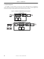 24
24
-
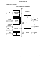 25
25
-
 26
26
-
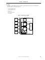 27
27
-
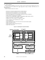 28
28
-
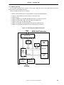 29
29
-
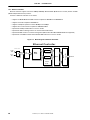 30
30
-
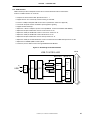 31
31
-
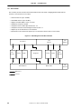 32
32
-
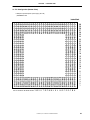 33
33
-
 34
34
-
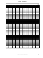 35
35
-
 36
36
-
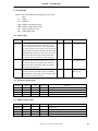 37
37
-
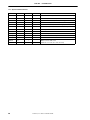 38
38
-
 39
39
-
 40
40
-
 41
41
-
 42
42
-
 43
43
-
 44
44
-
 45
45
-
 46
46
-
 47
47
-
 48
48
-
 49
49
-
 50
50
-
 51
51
-
 52
52
-
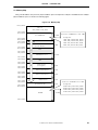 53
53
-
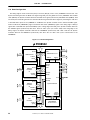 54
54
-
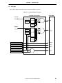 55
55
-
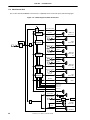 56
56
-
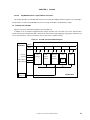 57
57
-
 58
58
-
 59
59
-
 60
60
-
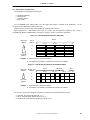 61
61
-
 62
62
-
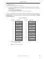 63
63
-
 64
64
-
 65
65
-
 66
66
-
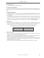 67
67
-
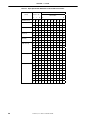 68
68
-
 69
69
-
 70
70
-
 71
71
-
 72
72
-
 73
73
-
 74
74
-
 75
75
-
 76
76
-
 77
77
-
 78
78
-
 79
79
-
 80
80
-
 81
81
-
 82
82
-
 83
83
-
 84
84
-
 85
85
-
 86
86
-
 87
87
-
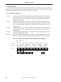 88
88
-
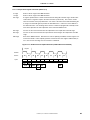 89
89
-
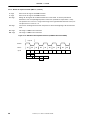 90
90
-
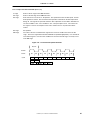 91
91
-
 92
92
-
 93
93
-
 94
94
-
 95
95
-
 96
96
-
 97
97
-
 98
98
-
 99
99
-
 100
100
-
 101
101
-
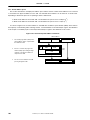 102
102
-
 103
103
-
 104
104
-
 105
105
-
 106
106
-
 107
107
-
 108
108
-
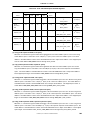 109
109
-
 110
110
-
 111
111
-
 112
112
-
 113
113
-
 114
114
-
 115
115
-
 116
116
-
 117
117
-
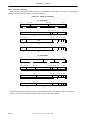 118
118
-
 119
119
-
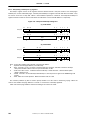 120
120
-
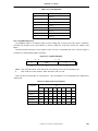 121
121
-
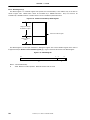 122
122
-
 123
123
-
 124
124
-
 125
125
-
 126
126
-
 127
127
-
 128
128
-
 129
129
-
 130
130
-
 131
131
-
 132
132
-
 133
133
-
 134
134
-
 135
135
-
 136
136
-
 137
137
-
 138
138
-
 139
139
-
 140
140
-
 141
141
-
 142
142
-
 143
143
-
 144
144
-
 145
145
-
 146
146
-
 147
147
-
 148
148
-
 149
149
-
 150
150
-
 151
151
-
 152
152
-
 153
153
-
 154
154
-
 155
155
-
 156
156
-
 157
157
-
 158
158
-
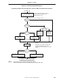 159
159
-
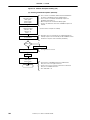 160
160
-
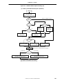 161
161
-
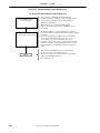 162
162
-
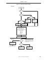 163
163
-
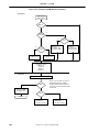 164
164
-
 165
165
-
 166
166
-
 167
167
-
 168
168
-
 169
169
-
 170
170
-
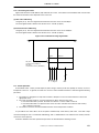 171
171
-
 172
172
-
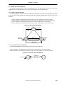 173
173
-
 174
174
-
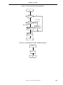 175
175
-
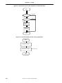 176
176
-
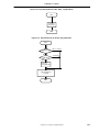 177
177
-
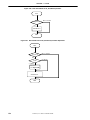 178
178
-
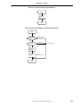 179
179
-
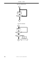 180
180
-
 181
181
-
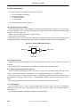 182
182
-
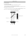 183
183
-
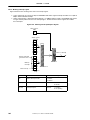 184
184
-
 185
185
-
 186
186
-
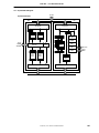 187
187
-
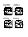 188
188
-
 189
189
-
 190
190
-
 191
191
-
 192
192
-
 193
193
-
 194
194
-
 195
195
-
 196
196
-
 197
197
-
 198
198
-
 199
199
-
 200
200
-
 201
201
-
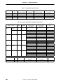 202
202
-
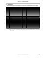 203
203
-
 204
204
-
 205
205
-
 206
206
-
 207
207
-
 208
208
-
 209
209
-
 210
210
-
 211
211
-
 212
212
-
 213
213
-
 214
214
-
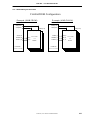 215
215
-
 216
216
-
 217
217
-
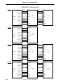 218
218
-
 219
219
-
 220
220
-
 221
221
-
 222
222
-
 223
223
-
 224
224
-
 225
225
-
 226
226
-
 227
227
-
 228
228
-
 229
229
-
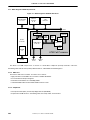 230
230
-
 231
231
-
 232
232
-
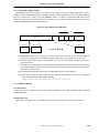 233
233
-
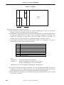 234
234
-
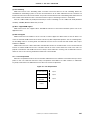 235
235
-
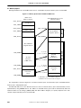 236
236
-
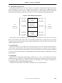 237
237
-
 238
238
-
 239
239
-
 240
240
-
 241
241
-
 242
242
-
 243
243
-
 244
244
-
 245
245
-
 246
246
-
 247
247
-
 248
248
-
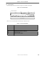 249
249
-
 250
250
-
 251
251
-
 252
252
-
 253
253
-
 254
254
-
 255
255
-
 256
256
-
 257
257
-
 258
258
-
 259
259
-
 260
260
-
 261
261
-
 262
262
-
 263
263
-
 264
264
-
 265
265
-
 266
266
-
 267
267
-
 268
268
-
 269
269
-
 270
270
-
 271
271
-
 272
272
-
 273
273
-
 274
274
-
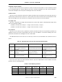 275
275
-
 276
276
-
 277
277
-
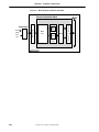 278
278
-
 279
279
-
 280
280
-
 281
281
-
 282
282
-
 283
283
-
 284
284
-
 285
285
-
 286
286
-
 287
287
-
 288
288
-
 289
289
-
 290
290
-
 291
291
-
 292
292
-
 293
293
-
 294
294
-
 295
295
-
 296
296
-
 297
297
-
 298
298
-
 299
299
-
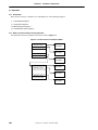 300
300
-
 301
301
-
 302
302
-
 303
303
-
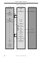 304
304
-
 305
305
-
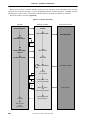 306
306
-
 307
307
-
 308
308
-
 309
309
-
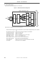 310
310
-
 311
311
-
 312
312
-
 313
313
-
 314
314
-
 315
315
-
 316
316
-
 317
317
-
 318
318
-
 319
319
-
 320
320
-
 321
321
-
 322
322
-
 323
323
-
 324
324
-
 325
325
-
 326
326
-
 327
327
-
 328
328
-
 329
329
-
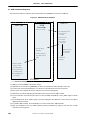 330
330
-
 331
331
-
 332
332
-
 333
333
-
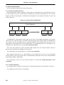 334
334
-
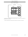 335
335
-
 336
336
-
 337
337
-
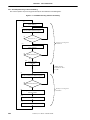 338
338
-
 339
339
-
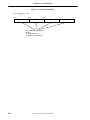 340
340
-
 341
341
-
 342
342
-
 343
343
-
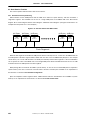 344
344
-
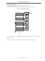 345
345
-
 346
346
-
 347
347
-
 348
348
-
 349
349
-
 350
350
-
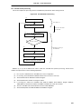 351
351
-
 352
352
-
 353
353
-
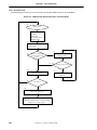 354
354
-
 355
355
-
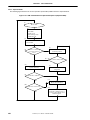 356
356
-
 357
357
-
 358
358
-
 359
359
-
 360
360
-
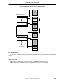 361
361
-
 362
362
-
 363
363
-
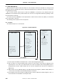 364
364
-
 365
365
-
 366
366
-
 367
367
-
 368
368
-
 369
369
-
 370
370
-
 371
371
-
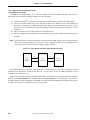 372
372
-
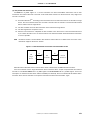 373
373
-
 374
374
-
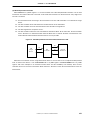 375
375
-
 376
376
-
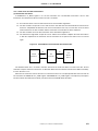 377
377
-
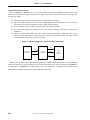 378
378
-
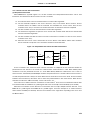 379
379
-
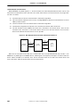 380
380
-
 381
381
-
 382
382
-
 383
383
-
 384
384
-
 385
385
-
 386
386
-
 387
387
-
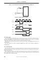 388
388
-
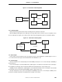 389
389
-
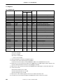 390
390
-
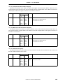 391
391
-
 392
392
-
 393
393
-
 394
394
-
 395
395
-
 396
396
-
 397
397
-
 398
398
-
 399
399
-
 400
400
-
 401
401
-
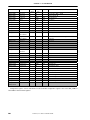 402
402
-
 403
403
-
 404
404
-
 405
405
-
 406
406
-
 407
407
-
 408
408
-
 409
409
-
 410
410
-
 411
411
-
 412
412
-
 413
413
-
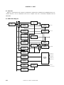 414
414
-
 415
415
-
 416
416
-
 417
417
-
 418
418
-
 419
419
-
 420
420
-
 421
421
-
 422
422
-
 423
423
-
 424
424
-
 425
425
-
 426
426
-
 427
427
-
 428
428
-
 429
429
-
 430
430
-
 431
431
-
 432
432
-
 433
433
-
 434
434
-
 435
435
-
 436
436
-
 437
437
-
 438
438
-
 439
439
-
 440
440
-
 441
441
-
 442
442
-
 443
443
-
 444
444
-
 445
445
-
 446
446
-
 447
447
-
 448
448
-
 449
449
-
 450
450
-
 451
451
-
 452
452
-
 453
453
-
 454
454
-
 455
455
-
 456
456
-
 457
457
-
 458
458
-
 459
459
-
 460
460
-
 461
461
-
 462
462
-
 463
463
-
 464
464
-
 465
465
-
 466
466
-
 467
467
-
 468
468
-
 469
469
-
 470
470
-
 471
471
-
 472
472
-
 473
473
-
 474
474
-
 475
475
-
 476
476
-
 477
477
-
 478
478
-
 479
479
-
 480
480
-
 481
481
-
 482
482
-
 483
483
-
 484
484
-
 485
485
-
 486
486
-
 487
487
-
 488
488
-
 489
489
-
 490
490
-
 491
491
-
 492
492
-
 493
493
-
 494
494
-
 495
495
-
 496
496
-
 497
497
-
 498
498
-
 499
499
-
 500
500
-
 501
501
-
 502
502
-
 503
503
-
 504
504
-
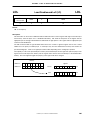 505
505
-
 506
506
-
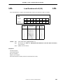 507
507
-
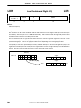 508
508
-
 509
509
-
 510
510
-
 511
511
-
 512
512
-
 513
513
-
 514
514
-
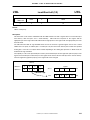 515
515
-
 516
516
-
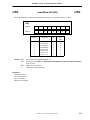 517
517
-
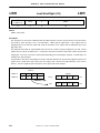 518
518
-
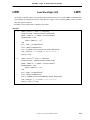 519
519
-
 520
520
-
 521
521
-
 522
522
-
 523
523
-
 524
524
-
 525
525
-
 526
526
-
 527
527
-
 528
528
-
 529
529
-
 530
530
-
 531
531
-
 532
532
-
 533
533
-
 534
534
-
 535
535
-
 536
536
-
 537
537
-
 538
538
-
 539
539
-
 540
540
-
 541
541
-
 542
542
-
 543
543
-
 544
544
-
 545
545
-
 546
546
-
 547
547
-
 548
548
-
 549
549
-
 550
550
-
 551
551
-
 552
552
-
 553
553
-
 554
554
-
 555
555
-
 556
556
-
 557
557
-
 558
558
-
 559
559
-
 560
560
-
 561
561
-
 562
562
-
 563
563
-
 564
564
-
 565
565
-
 566
566
-
 567
567
-
 568
568
-
 569
569
-
 570
570
-
 571
571
-
 572
572
-
 573
573
-
 574
574
-
 575
575
-
 576
576
-
 577
577
-
 578
578
-
 579
579
-
 580
580
-
 581
581
-
 582
582
-
 583
583
-
 584
584
-
 585
585
-
 586
586
-
 587
587
-
 588
588
-
 589
589
-
 590
590
-
 591
591
-
 592
592
-
 593
593
-
 594
594
-
 595
595


NEC Network Cables uPD98502 User manual
- Type
- User manual
- This manual is also suitable for
Ask a question and I''ll find the answer in the document
Finding information in a document is now easier with AI
Related papers
Other documents
-
NXP MPC8541E Reference guide
-
NXP MPC8560ADS Reference guide
-
NXP MPC8247 Reference guide
-
NXP MPC8275 Reference guide
-
-
Freescale Semiconductor MPC8265 User manual
-
Freescale Semiconductor MSC8144E Reference guide
-
NXP K60_100 Reference guide
-
-