
User’s Manual
µ
PD789488
µ
PD789489
µ
PD78F9488
µ
PD78F9489
µ
PD789489 Subseries
8-Bit Single-Chip Microcontrollers
Printed in Japan
Document No. U15331EJ4V1UD00 (4th edition)
Date Published July 2005 NS CP(K)
©

2 User’s Manual U15331EJ4V1UD
[MEMO]

User’s Manual U15331EJ4V1UD 3
1
2
3
4
VOLTAGE APPLICATION WAVEFORM AT INPUT PIN
Waveform distortion due to input noise or a reflected wave may cause malfunction. If the input of the
CMOS device stays in the area between V
IL (MAX) and VIH (MIN) due to noise, etc., the device may
malfunction. Take care to prevent chattering noise from entering the device when the input level is fixed,
and also in the transition period when the input level passes through the area between V
IL (MAX) and
V
IH (MIN).
HANDLING OF UNUSED INPUT PINS
Unconnected CMOS device inputs can be cause of malfunction. If an input pin is unconnected, it is
possible that an internal input level may be generated due to noise, etc., causing malfunction. CMOS
devices behave differently than Bipolar or NMOS devices. Input levels of CMOS devices must be fixed
high or low by using pull-up or pull-down circuitry. Each unused pin should be connected to V
DD or GND
via a resistor if there is a possibility that it will be an output pin. All handling related to unused pins must
be judged separately for each device and according to related specifications governing the device.
PRECAUTION AGAINST ESD
A strong electric field, when exposed to a MOS device, can cause destruction of the gate oxide and
ultimately degrade the device operation. Steps must be taken to stop generation of static electricity as
much as possible, and quickly dissipate it when it has occurred. Environmental control must be
adequate. When it is dry, a humidifier should be used. It is recommended to avoid using insulators that
easily build up static electricity. Semiconductor devices must be stored and transported in an anti-static
container, static shielding bag or conductive material. All test and measurement tools including work
benches and floors should be grounded. The operator should be grounded using a wrist strap.
Semiconductor devices must not be touched with bare hands. Similar precautions need to be taken for
PW boards with mounted semiconductor devices.
STATUS BEFORE INITIALIZATION
Power-on does not necessarily define the initial status of a MOS device. Immediately after the power
source is turned ON, devices with reset functions have not yet been initialized. Hence, power-on does
not guarantee output pin levels, I/O settings or contents of registers. A device is not initialized until the
reset signal is received. A reset operation must be executed immediately after power-on for devices
with reset functions.
POWER ON/OFF SEQUENCE
In the case of a device that uses different power supplies for the internal operation and external
interface, as a rule, switch on the external power supply after switching on the internal power supply.
When switching the power supply off, as a rule, switch off the external power supply and then the
internal power supply. Use of the reverse power on/off sequences may result in the application of an
overvoltage to the internal elements of the device, causing malfunction and degradation of internal
elements due to the passage of an abnormal current.
The correct power on/off sequence must be judged separately for each device and according to related
specifications governing the device.
INPUT OF SIGNAL DURING POWER OFF STATE
Do not input signals or an I/O pull-up power supply while the device is not powered. The current
injection that results from input of such a signal or I/O pull-up power supply may cause malfunction and
the abnormal current that passes in the device at this time may cause degradation of internal elements.
Input of signals during the power off state must be judged separately for each device and according to
related specifications governing the device.
NOTES FOR CMOS DEVICES
5
6

4 User’s Manual U15331EJ4V1UD
EEPROM and FIP are trademarks of NEC Electronics Corporation.
Windows and Windows NT are either registered trademarks or trademarks of Microsoft Corporation in the
United States and/or other countries.
PC/AT is a trademark of International Business Machines Corporation.
HP9000 series 700 and HP-UX are trademarks of Hewlett-Packard Company.
SPARCstation is a trademark of SPARC International, Inc.
Solaris and SunOS are trademarks of Sun Microsystems, Inc.
These commodities, technology or software, must be exported in accordance
with the export administration regulations of the exporting country.
Diversion contrary to the law of that country is prohibited.

User’s Manual U15331EJ4V1UD 5
The information in this document is current as of July, 2005. The information is subject to change
without notice. For actual design-in, refer to the latest publications of NEC Electronics data sheets or
data books, etc., for the most up-to-date specifications of NEC Electronics products. Not all
products and/or types are available in every country. Please check with an NEC Electronics sales
representative for availability and additional information.
No part of this document may be copied or reproduced in any form or by any means without the prior
written consent of NEC Electronics. NEC Electronics assumes no responsibility for any errors that may
appear in this document.
NEC Electronics does not assume any liability for infringement of patents, copyrights or other intellectual
property rights of third parties by or arising from the use of NEC Electronics products listed in this document
or any other liability arising from the use of such products. No license, express, implied or otherwise, is
granted under any patents, copyrights or other intellectual property rights of NEC Electronics or others.
Descriptions of circuits, software and other related information in this document are provided for illustrative
purposes in semiconductor product operation and application examples. The incorporation of these
circuits, software and information in the design of a customer's equipment shall be done under the full
responsibility of the customer. NEC Electronics assumes no responsibility for any losses incurred by
customers or third parties arising from the use of these circuits, software and information.
While NEC Electronics endeavors to enhance the quality, reliability and safety of NEC Electronics products,
customers agree and acknowledge that the possibility of defects thereof cannot be eliminated entirely. To
minimize risks of damage to property or injury (including death) to persons arising from defects in NEC
Electronics products, customers must incorporate sufficient safety measures in their design, such as
redundancy, fire-containment and anti-failure features.
NEC Electronics products are classified into the following three quality grades: "Standard", "Special" and
"Specific".
The "Specific" quality grade applies only to NEC Electronics products developed based on a customer-
designated "quality assurance program" for a specific application. The recommended applications of an NEC
Electronics product depend on its quality grade, as indicated below. Customers must check the quality grade of
each NEC Electronics product before using it in a particular application.
The quality grade of NEC Electronics products is "Standard" unless otherwise expressly specified in NEC
Electronics data sheets or data books, etc. If customers wish to use NEC Electronics products in applications
not intended by NEC Electronics, they must contact an NEC Electronics sales representative in advance to
determine NEC Electronics' willingness to support a given application.
(Note)
•
•
•
•
•
•
M8E 02. 11-1
(1)
(2)
"NEC Electronics" as used in this statement means NEC Electronics Corporation and also includes its
majority-owned subsidiaries.
"NEC Electronics products" means any product developed or manufactured by or for NEC Electronics (as
defined above).
Computers, office equipment, communications equipment, test and measurement equipment, audio
and visual equipment, home electronic appliances, machine tools, personal electronic equipment
and industrial robots.
Transportation equipment (automobiles, trains, ships, etc.), traffic control systems, anti-disaster
systems, anti-crime systems, safety equipment and medical equipment (not specifically designed
for life support).
Aircraft, aerospace equipment, submersible repeaters, nuclear reactor control systems, life
support systems and medical equipment for life support, etc.
"Standard":
"Special":
"Specific":

6 User’s Manual U15331EJ4V1UD
Regional Information
•
Device availability
•
Ordering information
•
Product release schedule
•
Availability of related technical literature
•
Development environment specifications (for example, specifications for third-party tools and
components, host computers, power plugs, AC supply voltages, and so forth)
•
Network requirements
In addition, trademarks, registered trademarks, export restrictions, and other legal issues may also vary
from country to country.
[GLOBAL SUPPORT]
http://www.necel.com/en/support/support.html
NEC Electronics America, Inc. (U.S.)
Santa Clara, California
Tel: 408-588-6000
800-366-9782
NEC Electronics Hong Kong Ltd.
Hong Kong
Tel: 2886-9318
NEC Electronics Hong Kong Ltd.
Seoul Branch
Seoul, Korea
Tel: 02-558-3737
NEC Electronics Shanghai Ltd.
Shanghai, P.R. China
Tel: 021-5888-5400
NEC Electronics Taiwan Ltd.
Taipei, Taiwan
Tel: 02-2719-2377
NEC Electronics Singapore Pte. Ltd.
Novena Square, Singapore
Tel: 6253-8311
J05.6
N
EC Electronics (Europe) GmbH
Duesseldorf, Germany
Tel: 0211-65030
•
Sucursal en España
Madrid, Spain
Tel: 091-504 27 87
Vélizy-Villacoublay, France
Tel: 01-30-67 58 00
•
Succursale Française
•
Filiale Italiana
Milano, Italy
Tel: 02-66 75 41
•
Branch The Netherlands
Eindhoven, The Netherlands
Tel: 040-265 40 10
•
Tyskland Filial
Taeby, Sweden
Tel: 08-63 87 200
•
United Kingdom Branch
Milton Keynes, UK
Tel: 01908-691-133
Some information contained in this document may vary from country to country. Before using any NEC
Electronics product in your application, pIease contact the NEC Electronics office in your country to
obtain a list of authorized representatives and distributors. They will verify:

User’s Manual U15331EJ4V1UD 7
Major Revisions in This Edition
Page Description
Throughout Change of descriptions of
µ
PD789489, 78F9489
• Change of status from under development to development completed
• Change of the subseries name to “
µ
PD789489 subseries”
pp.31 to 33 Update of 1.5 78K/0S Series Lineup to latest version
p.123 Modification of Figure 7-2 Block Diagram of Timer 50
p.124 Modification of Figure 7-3 Block Diagram of Timer 60
Modification of Figure 7-5 Block Diagram of Output control circuit (Timer 60) p.126
Addition of descriptions in 7.2 (2) 8-bit compare register 60
p.127 Addition of descriptions in 7.2 (4) 8-bit H width compare registers 60 and 61
p.136 Modification of Figure 7-11 8-bit Timing of Interval Timer Operation with 8-Bit Resolution (Basic Operation)
p.137 Modification of Figure 7-13. Timing of Interval Timer Operation with 8-Bit Resolution (When CRnm Is Set to
FFH)
p.140 Modification of Figure 7-17. Timing of Operation of External Event Counter with 8-Bit Resolution
p.150 Addition of descriptions of setting sequence in 7.4.3 Operation as carrier generator
p.151 Modification of Figure 7-22. Timing of Carrier Generator Operation (When CR60 = N, CRH60 = M (M > N))
p.152 Modification of Figure 7-23. Timing of Carrier Generator Operation (When CR60 = N, CRH60 = M (M < N))
p.153 Modification of Figure 7-24. Timing of Carrier Generator Operation (When CR60 = CRH60 = N)
pp.154 to
157
Modification of the mode name in 7.4.4 PWM output mode operation (timer 50)
pp.158, 159 Modification of the mode name in 7.4.5 PPG output mode operation (timer 60 and 61)
p.160 Modification of (1) Error on starting timer in 7.5 Cautions on Using 8-Bit Timers 50, 60, and 61
p.174 Modification of Figure 10-1. Block Diagram of 10-bit A/D converter
p.182 Modification of (1) Current consumption in standby mode in 10.5 Cautions Related to 10-Bit A/D Converter
p.187 Modification of Figure 11-1. Block Diagram of Serial Interface 20
p.190 Addition of Caution in Figure 11-3 Format of Serial Operation Mode Register 20
p.194 Modification of Cautions in Figure 11-6 Format of Baud Rate Generator Control Register 20
pp.195, 203 Modification of Caution in Table 11-3 and 11-5. Example of Relationship Between System Clock and Baud
Rate
p.222 Modification of descriptions in Figure 12-4. Format of Automatic Data Transmit/Receive Interval
Specification Register 0
pp.342 to
361
Addition of formal specifications of
µ
PD789489 and 78F9489 in CHAPTER 22 ELECTRICAL SPECIFICATIONS
(
µ
PD789488, 78F9488, 789489, 78F9489)
pp.366, 367 Addition of recommended conditions for
µ
PD789489 and 78F9489 in CHAPTER 25 RECOMMENDED
SOLDERING CONDITIONS
Major Revisions in Modified Edition (U15331EJ4V1UD00)
Throughout Addition of the lead-free products
pp.254, 257 Modification of descriptions of the voltage boost wait time in CHAPTER 13 LCD CONTROLLER/DRIVER
pp.328 Modification of Figure 19-9. Wiring Example for Flash Writing Adapter with 3-Wire Serial I/O with
Handshake
The mark shows major revised points.

8 User’s Manual U15331EJ4V1UD
INTRODUCTION
Target Readers This manual is intended for user engineers who wish to understand the functions of
the
µ
PD789489 Subseries and design and develop application systems and programs
for these devices.
Target products:
•
µ
PD789489 Subseries:
µ
PD789488, 789489, 78F9488, 78F9489
Purpose This manual is intended to give users an understanding of the functions described in
the Organization below.
Organization Two manuals are available for the
µ
PD789489 Subseries:
This manual and the instruction manual (common to the 78K/0S Series).
µ
PD789489 Subseries
User’s Manual
78K/0S Series
User’s Manual
Instructions
• Pin functions
• Internal block functions
• Interrupts
• Other on-chip peripheral functions
• Electrical specifications
• CPU function
• Instruction set
• Instruction description
How to Use This Manual It is assumed that the readers of this manual have general knowledge of electrical
engineering, logic circuits, and microcontrollers.
• To understand the overall functions of the
µ
PD789489 Subseries
→ Read this manual in the order of the CONTENTS.
• How to read register formats
→ The name of a bit whose number is enclosed with <> is reserved in the
assembler and is defined as an sfr variable by the #pragma sfr directive for the
C compiler.
• To learn the detailed functions of a register whose register name is known
→ See APPENDIX C REGISTER INDEX.
• To learn the details of the instruction functions of the 78K/0S series
→ Refer to 78K/0S Series Instructions User’s Manual (U11047E) separately
available.
• To learn about the electrical specifications of the
µ
PD789489 Subseries
→ Refer to CHAPTER 22 ELECTRICAL SPECIFICATIONS (
µ
PD789488,
78F9488, 789489, 78F9489)

User’s Manual U15331EJ4V1UD 9
Conventions Data significance: Higher digits on the left and lower digits on the right
Active low representation: xxx (overscore over pin or signal name)
Note: Footnote for item marked with Note in the text
Caution: Information requiring particular attention
Remark: Supplementary information
Numerical representation: Binary ... xxxx or xxxxB
Decimal ... xxxx
Hexadecimal ... xxxxH
Related Documents The related documents indicated in this publication may include preliminary versions.
However, preliminary versions are not marked as such.
Documents Related to Devices
Document Name Document No.
µ
PD789489 Subseries User’s Manual This manual
78K/0S Series Instructions User’s Manual U11047E
Documents Related to Development Software Tools (User’s Manuals)
Document Name Document No.
Operation U17391E
Language U17390E
RA78K0S Assembler Package
Structured Assembly Language U17389E
Operation U16654E CC78K0S C Compiler
Language U16655E
Operation U17246E SM+ System Simulator
User Open Interface U17247E
Operation U16768E SM78K Series Ver. 2.52 System Simulator
External Part User Open Interface Specification U15802E
ID78K0S-NS Ver. 2.52 Integrated Debugger Operation U16584E
PM plus Ver.5.20 U16934E
Documents Related to Development Tools (Hardware) (User’s Manuals)
Document Name Document No.
IE-78K0S-NS In-Circuit Emulator U13549E
IE-78K0S-NS-A In-Circuit Emulator U15207E
IE-789488-NS-EM1 Emulation Board U16492E
Caution The related documents listed above are subject to change without notice. Be sure to use the latest
version of each document for designing.

10 User’s Manual U15331EJ4V1UD
Documents Related to Flash Memory Writing
Document Name Document No.
PG-FP3 Flash Memory Programmer User’s Manual U13502E
PG-FP4 Flash Memory Programmer User’s Manual U15260E
Other Related Documents
Document Name Document No.
SEMICONDUCTOR SELECTION GUIDE - Products and Packages - X13769X
Semiconductor Device Mount Manual Note
Quality Grades on NEC Semiconductor Devices C11531E
NEC Semiconductor Device Reliability/Quality Control System C10983E
Guide to Prevent Damage for Semiconductor Devices by Electrostatic Discharge (ESD) C11892E
Note See the “Semiconductor Device Mount Manual” website (http://www.necel.com/pkg/en/mount/index.html)
Caution The related documents listed above are subject to change without notice. Be sure to use the
latest version of each document for designing.

User’s Manual U15331EJ4V1UD 11
CONTENTS
CHAPTER 1 GENERAL .......................................................................................................................... 26
1.1 Features ......................................................................................................................................26
1.2 Applications ...............................................................................................................................26
1.3 Ordering Information ................................................................................................................. 27
1.4 Pin Configuration (Top View) ................................................................................................... 28
1.5 78K/0S Series Lineup ................................................................................................................31
1.6 Block Diagram............................................................................................................................34
1.7 Overview of Functions .............................................................................................................. 35
CHAPTER 2 PIN FUNCTIONS............................................................................................................... 37
2.1 List of Pin Functions .................................................................................................................37
2.2 Description of Pin Functions....................................................................................................40
2.2.1 P00 to P07 (Port 0) ....................................................................................................................... 40
2.2.2 P10, P11 (Port 1) .......................................................................................................................... 40
2.2.3 P20 to P25 (Port 2) ....................................................................................................................... 40
2.2.4 P30 to P34 (Port 3) ....................................................................................................................... 41
2.2.5 P50 to P53 (Port 5) ....................................................................................................................... 41
2.2.6 P60 to P67 (Port 6) ....................................................................................................................... 42
2.2.7 P70 to P73 (Port 7) ....................................................................................................................... 42
2.2.8 P80 to P87 (Port 8) ....................................................................................................................... 42
2.2.9 S0 to S27 ...................................................................................................................................... 42
2.2.10 COM0 to COM3 ............................................................................................................................ 42
2.2.11 V
LC0 to VLC2 ................................................................................................................................... 42
2.2.12 CAPH, CAPL................................................................................................................................. 42
2.2.13 RESET.......................................................................................................................................... 43
2.2.14 X1, X2 ........................................................................................................................................... 43
2.2.15 XT1, XT2....................................................................................................................................... 43
2.2.16 AV
DD.............................................................................................................................................. 43
2.2.17 AV
SS .............................................................................................................................................. 43
2.2.18 V
DD ................................................................................................................................................ 43
2.2.19 V
SS ................................................................................................................................................ 43
2.2.20 V
PP (flash memory version only).................................................................................................... 43
2.2.21 IC0 (mask ROM version only) ....................................................................................................... 44
2.3 Pin I/O Circuits and Recommended Connection of Unused Pins ........................................45
CHAPTER 3 CPU ARCHITECTURE......................................................................................................48
3.1 Memory Space............................................................................................................................48
3.1.1 Internal program memory space ................................................................................................... 52
3.1.2 Internal data memory space.......................................................................................................... 53
3.1.3 Special function register (SFR) area ............................................................................................. 53

12 User’s Manual U15331EJ4V1UD
3.1.4 Data memory addressing ..............................................................................................................54
3.2 Processor Registers ..................................................................................................................58
3.2.1 Control registers............................................................................................................................58
3.2.2 General-purpose registers.............................................................................................................61
3.2.3 Special function registers (SFRs).................................................................................................. 62
3.3 Instruction Address Addressing ..............................................................................................66
3.3.1 Relative addressing.......................................................................................................................66
3.3.2 Immediate addressing................................................................................................................... 67
3.3.3 Table indirect addressing ..............................................................................................................68
3.3.4 Register addressing ......................................................................................................................68
3.4 Operand Address Addressing ..................................................................................................69
3.4.1 Direct addressing .......................................................................................................................... 69
3.4.2 Short direct addressing .................................................................................................................70
3.4.3 Special function register (SFR) addressing ...................................................................................71
3.4.4 Register addressing ......................................................................................................................72
3.4.5 Register indirect addressing.......................................................................................................... 73
3.4.6 Based addressing ......................................................................................................................... 74
3.4.7 Stack addressing........................................................................................................................... 74
CHAPTER 4 PORT FUNCTIONS ...........................................................................................................75
4.1 Port Functions............................................................................................................................75
4.2 Port Configuration .....................................................................................................................76
4.2.1 Port 0 ............................................................................................................................................ 77
4.2.2 Port 1 ............................................................................................................................................ 78
4.2.3 Port 2 ............................................................................................................................................ 79
4.2.4 Port 3 ............................................................................................................................................ 84
4.2.5 Port 5 ............................................................................................................................................ 86
4.2.6 Port 6 ............................................................................................................................................ 87
4.2.7 Port 7 ............................................................................................................................................ 89
4.2.8 Port 8 ............................................................................................................................................ 90
4.3 Registers Controlling Port Function ........................................................................................91
4.4 Port Function Operation............................................................................................................94
4.4.1 Writing to I/O port ..........................................................................................................................94
4.4.2 Reading from I/O port.................................................................................................................... 94
4.4.3 Arithmetic operation of I/O port ..................................................................................................... 94
CHAPTER 5 CLOCK GENERATOR ......................................................................................................95
5.1 Clock Generator Functions.......................................................................................................95
5.2 Clock Generator Configuration ................................................................................................95
5.3 Registers Controlling Clock Generator ...................................................................................98
5.4 System Clock Oscillators........................................................................................................101
5.4.1 Main system clock oscillator........................................................................................................ 101
5.4.2 Subsystem clock oscillator ..........................................................................................................102
5.4.3 Example of incorrect resonator connection ................................................................................. 103
5.4.4 Divider circuit...............................................................................................................................104

User’s Manual U15331EJ4V1UD 13
5.4.5 When subsystem clock is not used ............................................................................................. 104
5.4.6 Subsystem clock ×4 multiplication circuit .................................................................................... 104
5.5 Clock Generator Operation.....................................................................................................105
5.6 Changing Setting of System Clock and CPU Clock .............................................................106
5.6.1 Time required for switching between system clock and CPU clock............................................. 106
5.6.2 Switching between system clock and CPU clock ........................................................................ 107
CHAPTER 6 16-BIT TIMER 20............................................................................................................108
6.1 16-Bit Timer 20 Functions.......................................................................................................108
6.2 16-Bit Timer 20 Configuration ................................................................................................108
6.3 Registers Controlling 16-Bit Timer 20 ...................................................................................110
6.4 16-Bit Timer 20 Operation .......................................................................................................113
6.4.1 Operation as timer interrupt ........................................................................................................ 113
6.4.2 Operation as timer output............................................................................................................ 115
6.4.3 Capture operation ....................................................................................................................... 116
6.4.4 16-bit timer counter 20 readout ................................................................................................... 117
6.5 Cautions on Using 16-Bit Timer 20 ........................................................................................118
6.5.1 Restrictions when rewriting 16-bit compare register 20............................................................... 118
CHAPTER 7 8-BIT TIMERS 50, 60, AND 61 ...................................................................................120
7.1 Functions of 8-Bit Timers 50, 60, and 61 ...............................................................................120
7.2 Configuration of 8-Bit Timers 50, 60, and 61 ........................................................................122
7.3 Control Registers for 8-Bit Timers 50, 60, and 61 ................................................................128
7.4 Operation of 8-Bit Timers 50, 60, and 61 ............................................................................... 134
7.4.1 Operation as 8-bit timer counter.................................................................................................. 134
7.4.2 Operation as 16-bit timer counter................................................................................................ 143
7.4.3 Operation as carrier generator .................................................................................................... 150
7.4.4 PWM output mode operation (timer 50) ...................................................................................... 154
7.4.5 PPG output mode operation (timer 60 and timer 61)................................................................... 158
7.5 Cautions on Using 8-Bit Timers 50, 60, and 61.....................................................................160
CHAPTER 8 WATCH TIMER ...............................................................................................................161
8.1 Watch Timer Functions ...........................................................................................................161
8.2 Configuration of Watch Timer ................................................................................................162
8.3 Control Registers for Watch Timer ........................................................................................163
8.4 Watch Timer Operation ...........................................................................................................165
8.4.1 Operation as watch timer ............................................................................................................ 165
8.4.2 Operation as interval timer .......................................................................................................... 165
CHAPTER 9 WATCHDOG TIMER .......................................................................................................167
9.1 Watchdog Timer Functions ....................................................................................................167
9.2 Watchdog Timer Configuration ..............................................................................................168
9.3 Watchdog Timer Control Registers .......................................................................................169
9.4 Watchdog Timer Operation.....................................................................................................171

14 User’s Manual U15331EJ4V1UD
9.4.1 Operation as watchdog timer ...................................................................................................... 171
9.4.2 Operation as interval timer ..........................................................................................................172
CHAPTER 10 10-BIT A/D CONVERTER ............................................................................................173
10.1 10-Bit A/D Converter Functions..............................................................................................173
10.2 10-Bit A/D Converter Configuration .......................................................................................173
10.3 10-Bit A/D Converter Control Registers ................................................................................176
10.4 10-Bit A/D Converter Operation..............................................................................................178
10.4.1 Basic operation of 10-bit A/D converter....................................................................................... 178
10.4.2 Input voltage and conversion result............................................................................................. 179
10.4.3 Operation mode of 10-bit A/D converter...................................................................................... 181
10.5 Cautions Related to 10-Bit A/D Converter.............................................................................182
CHAPTER 11 SERIAL INTERFACE 20 ..............................................................................................186
11.1 Serial Interface 20 Functions ..................................................................................................186
11.2 Serial Interface 20 Configuration............................................................................................186
11.3 Serial Interface 20 Control Registers.....................................................................................190
11.4 Serial Interface 20 Operation ..................................................................................................197
11.4.1 Operation stop mode................................................................................................................... 197
11.4.2 Asynchronous serial interface (UART) mode ..............................................................................199
11.4.3 3-wire serial I/O mode .................................................................................................................211
CHAPTER 12 SERIAL INTERFACE 1A0 ...........................................................................................216
12.1 Function of Serial Interface 1A0 .............................................................................................216
12.2 Configuration of Serial Interface 1A0.....................................................................................217
12.3 Control Registers for Serial Interface 1A0 ............................................................................219
12.4 Serial Interface 1A0 Operation................................................................................................224
12.4.1 Operation stop mode................................................................................................................... 224
12.4.2 3-wire serial I/O mode .................................................................................................................225
12.4.3 3-wire serial I/O mode with automatic transmit/receive function.................................................. 230
CHAPTER 13 LCD CONTROLLER/DRIVER.......................................................................................250
13.1 LCD Controller/Driver Functions............................................................................................250
13.2 LCD Controller/Driver Configuration .....................................................................................250
13.3 Registers Controlling LCD Controller/Driver ........................................................................253
13.4 Setting LCD Controller/Driver.................................................................................................257
13.5 LCD Display Data Memory ......................................................................................................257
13.6 Common and Segment Signals ..............................................................................................258
13.7 Display Modes ..........................................................................................................................260
13.7.1 Three-time-slice display example................................................................................................260
13.7.2 Four-time-slice display example.................................................................................................. 263
13.8 Supplying LCD Drive Voltages VLC0, VLC1, and VLC2 .............................................................266
CHAPTER 14 MULTIPLIER ..................................................................................................................267

User’s Manual U15331EJ4V1UD 15
14.1 Multiplier Function...................................................................................................................267
14.2 Multiplier Configuration ..........................................................................................................267
14.3 Multiplier Control Register......................................................................................................269
14.4 Multiplier Operation .................................................................................................................270
CHAPTER 15 REMOTE CONTROLLER RECEIVER (
µ
PD789489, 78F9489 ONLY)......................271
15.1 Remote Controller Receiver Functions .................................................................................271
15.2 Remote Controller Receiver Configuration........................................................................... 271
15.3 Registers to Control Remote Controller Receiver................................................................277
15.4 Operation of Remote Controller Receiver ............................................................................. 279
15.4.1 Format of type A reception mode................................................................................................ 279
15.4.2 Operation flow of type A reception mode .................................................................................... 279
15.4.3 Timing ......................................................................................................................................... 281
15.4.4 Compare register setting............................................................................................................. 283
15.4.5 Error interrupt generation timing ................................................................................................. 285
15.4.6 Noise elimination......................................................................................................................... 287
CHAPTER 16 INTERRUPT FUNCTIONS ............................................................................................290
16.1 Interrupt Function Types.........................................................................................................290
16.2 Interrupt Sources and Configuration.....................................................................................290
16.3 Registers Controlling Interrupt Function ..............................................................................294
16.4 Interrupt Servicing Operation .................................................................................................301
16.4.1 Non-maskable interrupt request acknowledgment operation ...................................................... 301
16.4.2 Maskable interrupt request acknowledgment operation .............................................................. 303
16.4.3 Multiple interrupt servicing .......................................................................................................... 304
16.4.4 Putting interrupt requests on hold ............................................................................................... 306
CHAPTER 17 STANDBY FUNCTION..................................................................................................307
17.1 Standby Function and Configuration ....................................................................................307
17.1.1 Standby function ......................................................................................................................... 307
17.1.2 Register controlling standby function .......................................................................................... 308
17.2 Standby Function Operation...................................................................................................309
17.2.1 HALT mode................................................................................................................................. 309
17.2.2 STOP mode ................................................................................................................................ 312
CHAPTER 18 RESET FUNCTION .......................................................................................................315
CHAPTER 19 FLASH MEMORY VERSION .......................................................................................319
19.1 Flash Memory Characteristics................................................................................................320
19.1.1 Programming environment.......................................................................................................... 320
19.1.2 Communication mode ................................................................................................................. 321
19.1.3 On-board pin processing............................................................................................................. 324
19.1.4 Connection of adapter for flash writing........................................................................................ 327
19.2 Cautions on
µ
PD78F9488 and 78F9489 ................................................................................. 330

16 User’s Manual U15331EJ4V1UD
CHAPTER 20 MASK OPTIONS ...........................................................................................................331
CHAPTER 21 INSTRUCTION SET ......................................................................................................332
21.1 Operation ..................................................................................................................................332
21.1.1 Operand identifiers and description methods .............................................................................. 332
21.1.2 Description of “Operation” column............................................................................................... 333
21.1.3 Description of “Flag” column ....................................................................................................... 333
21.2 Operation List...........................................................................................................................334
21.3 Instructions Listed by Addressing Type ...............................................................................339
CHAPTER 22 ELECTRICAL SPECIFICATIONS (
µ
PD789488, 78F9488, 789489, 78F9489) ..........342
CHAPTER 23 CHARACTERISTICS CURVES OF LCD CONTROLLER/DRIVER ..............................362
CHAPTER 24 PACKAGE DRAWINGS.................................................................................................364
CHAPTER 25 RECOMMENDED SOLDERING CONDITIONS...........................................................366
APPENDIX A DEVELOPMENT TOOLS...............................................................................................369
A.1 Software Package ....................................................................................................................371
A.2 Language Processing Software .............................................................................................371
A.3 Control Software ......................................................................................................................372
A.4 Flash Memory Writing Tools ...................................................................................................372
A.5 Debugging Tools (Hardware)..................................................................................................373
A.6 Debugging Tools (Software) ...................................................................................................374
APPENDIX B NOTES ON TARGET SYSTEM DESIGN ...................................................................375
APPENDIX C REGISTER INDEX .........................................................................................................379
C.1 Register Index (Register Names in Alphabetic Order) .........................................................379
C.2 Register Index (Register Symbols Alphabetic Order) ..........................................................382
APPENDIX D REVISION HISTORY ......................................................................................................385

User’s Manual U15331EJ4V1UD 17
LIST OF FIGURES (1/6)
Figure No. Title Page
2-1 I/O Circuit Types ..........................................................................................................................................46
3-1 Memory Map (
µ
PD789488)..........................................................................................................................48
3-2 Memory Map (
µ
PD78F9488)........................................................................................................................49
3-3 Memory Map (
µ
PD789489)..........................................................................................................................50
3-4 Memory Map (
µ
PD78F9489)........................................................................................................................51
3-5 Data Memory Addressing (
µ
PD789488) ......................................................................................................54
3-6 Data Memory Addressing (
µ
PD78F9488) ....................................................................................................55
3-7 Data Memory Addressing (
µ
PD789489) ......................................................................................................56
3-8 Data Memory Addressing (
µ
PD78F9489) ....................................................................................................57
3-9 Program Counter Configuration ...................................................................................................................58
3-10 Program Status Word Configuration ............................................................................................................58
3-11 Stack Pointer Configuration .........................................................................................................................60
3-12 Data to Be Saved to Stack Memory .............................................................................................................60
3-13 Data to Be Restored from Stack Memory.....................................................................................................60
3-14 General-Purpose Register Configuration .....................................................................................................61
4-1 Port Types....................................................................................................................................................75
4-2 Block Diagram of P00 to P07 .......................................................................................................................77
4-3 Block Diagram of P10 and P11 ....................................................................................................................78
4-4 Block Diagram of P20 ..................................................................................................................................79
4-5 Block Diagram of P21 ..................................................................................................................................80
4-6 Block Diagram of P22 and P25 ....................................................................................................................81
4-7 Block Diagram of P23 ..................................................................................................................................82
4-8 Block Diagram of P24 ..................................................................................................................................83
4-9 Block Diagram of P30 to P33 .......................................................................................................................84
4-10 Block Diagram of P34 ..................................................................................................................................85
4-11 Block Diagram of P50 to P53 .......................................................................................................................86
4-12 Block Diagram of P60 to P67 .......................................................................................................................87
4-13 Block Diagram of P70 to P73 .......................................................................................................................89
4-14 Block Diagram of P80 to P87 .......................................................................................................................90
4-15 Port Mode Register Format..........................................................................................................................91
4-16 Format of Pull-Up Resistor Option Registers ...............................................................................................93
4-17 Port Function Register Format .....................................................................................................................93
5-1 Clock Generator Block Diagram (
µ
PD789488, 789489)...............................................................................96
5-2 Clock Generator Block Diagram (
µ
PD78F9488, 78F9489) ..........................................................................97
5-3 Format of Processor Clock Control Register................................................................................................98
5-4 Format of Subclock Oscillation Mode Register.............................................................................................99

18 User’s Manual U15331EJ4V1UD
LIST OF FIGURES (2/6)
Figure No. Title Page
5-5 Format of Subclock Control Register............................................................................................................99
5-6 Subclock Selection Register Format ..........................................................................................................100
5-7 External Circuit of Main System Clock Oscillator........................................................................................101
5-8 External Circuit of Subsystem Clock Oscillator...........................................................................................102
5-9 Examples of Incorrect Resonator Connection ............................................................................................103
5-10 Switching Between System Clock and CPU Clock.....................................................................................107
6-1 Block Diagram of 16-Bit Timer 20 ..............................................................................................................109
6-2 Format of 16-Bit Timer Mode Control Register 20......................................................................................111
6-3 Format of Port Mode Register 3 .................................................................................................................112
6-4 Settings of 16-Bit Timer Mode Control Register 20 for Timer Interrupt Operation......................................113
6-5 Timing of Timer Interrupt Operation ...........................................................................................................114
6-6 Settings of 16-Bit Timer Mode Control Register 20 for Timer Output Operation ........................................115
6-7 Timer Output Timing ..................................................................................................................................115
6-8 Settings of 16-Bit Timer Mode Control Register 20 for Capture Operation.................................................116
6-9 Capture Operation Timing (with Both Edges of CPT20 Pin Specified) .......................................................116
6-10 16-Bit Timer Counter 20 Readout Timing...................................................................................................117
7-1 Block Diagram of 24-Bit Event Counter......................................................................................................121
7-2 Block Diagram of Timer 50.........................................................................................................................123
7-3 Block Diagram of Timer 60.........................................................................................................................124
7-4 Block Diagram of Timer 61.........................................................................................................................125
7-5 Block Diagram of Output Controller (Timer 60) ..........................................................................................126
7-6 Format of 8-Bit Timer Mode Control Register 50 .......................................................................................128
7-7 Format of 8-Bit Timer Mode Control Register 60........................................................................................130
7-8 Format of Carrier Generator Output Control Register 60 ...........................................................................131
7-9 Format of 8-Bit Timer Mode Control Register 61........................................................................................132
7-10 Format of Port Mode Register 3 .................................................................................................................133
7-11 Timing of Interval Timer Operation with 8-Bit Resolution (Basic Operation)...............................................136
7-12 Timing of Interval Timer Operation with 8-Bit Resolution (When CRnm Is Set to 00H)..............................136
7-13 Timing of Interval Timer Operation with 8-Bit Resolution (When CRnm Is Set to FFH)..............................137
7-14 Timing of Interval Timer Operation with 8-Bit Resolution (When CRnm Changes from N to M (N < M))....137
7-15 Timing of Interval Timer Operation with 8-Bit Resolution (When CRnm Changes from N to M (N > M))....138
7-16 Timing of Interval Timer Operation with 8-Bit Resolution (When Timer 60 Match Signal Is Selected
for Timer 50 Count Clock) ..........................................................................................................................139
7-17 Timing of Operation of External Event Counter with 8-Bit Resolution ........................................................140
7-18 Timing of Square-Wave Output with 8-Bit Resolution ................................................................................142
7-19 Timing of Interval Timer Operation with 16-Bit Resolution .........................................................................145
7-20 Timing of External Event Counter Operation with 16-Bit Resolution ..........................................................147

User’s Manual U15331EJ4V1UD 19
LIST OF FIGURES (3/6)
Figure No. Title Page
7-21 Timing of Square-Wave Output with 16-Bit Resolution ..............................................................................149
7-22 Timing of Carrier Generator Operation (When CR60 = N, CRH60 = M (M > N))........................................151
7-23 Timing of Carrier Generator Operation (When CR60 = N, CRH60 = M (M < N))........................................152
7-24 Timing of Carrier Generator Operation (When CR60 = CRH60 = N) .........................................................153
7-25 Operation Timing in PWM Output Mode (When Rising Edge Is Selected).................................................154
7-26 Operation Timing When Overwriting CR50 (When Rising Edge Is Selected).............................................155
7-27 Operation Timing in PWM Output Mode (When Both Edges Are Selected)...............................................156
7-28 Operation Timing in PWM Output Mode (When Both Edges Are Selected)
(When CR50 Is Overwritten) ......................................................................................................................157
7-29 PPG Output Mode Timing (Basic Operation) .............................................................................................159
7-30 PPG Output Mode Timing (When CR6m and CRH6m Are Overwritten)....................................................159
7-31 Case in Which Error of 1.5 Clocks (Max.) Occurs......................................................................................160
7-32 Timing of Operation as External Event Counter (8-Bit Resolution) ............................................................160
8-1 Block Diagram of Watch Timer ..................................................................................................................161
8-2 Format of Watch Timer Mode Control Register..........................................................................................163
8-3 Format of Watch Timer Interrupt Time Selection Register .........................................................................164
8-4 Watch Timer/Interval Timer Operation Timing ...........................................................................................166
9-1 Block Diagram of Watchdog Timer.............................................................................................................168
9-2 Format of Watchdog Timer Clock Selection Register.................................................................................169
9-3 Format of Watchdog Timer Mode Register ................................................................................................170
10-1 Block Diagram of 10-Bit A/D Converter......................................................................................................174
10-2 Format of A/D Converter Mode Register 0.................................................................................................176
10-3 Format of Analog Input Channel Specification Register 0..........................................................................177
10-4 Basic Operation of 10-Bit A/D Converter....................................................................................................179
10-5 Relationship Between Analog Input Voltage and A/D Conversion Result ..................................................180
10-6 Software-Started A/D Conversion ..............................................................................................................181
10-7 How to Reduce Current Consumption in Standby Mode ............................................................................182
10-8 Conversion Result Read Timing (if Conversion Result Is Undefined) ........................................................183
10-9 Conversion Result Read Timing (if Conversion Result Is Normal) .............................................................183
10-10 Analog Input Pin Handling..........................................................................................................................184
10-11 A/D Conversion End Interrupt Request Generation Timing........................................................................185
10-12 AV
DD Pin Handling......................................................................................................................................185
11-1 Block Diagram of Serial Interface 20..........................................................................................................187
11-2 Bock Diagram of Baud Rate Generator 20.................................................................................................188
11-3 Format of Serial Operation Mode Register 20............................................................................................190

20 User’s Manual U15331EJ4V1UD
LIST OF FIGURES (4/6)
Figure No. Title Page
11-4 Format of Asynchronous Serial Interface Mode Register 20 ......................................................................191
11-5 Format of Asynchronous Serial Interface Status Register 20.....................................................................193
11-6 Format of Baud Rate Generator Control Register 20 .................................................................................194
11-7 Format of Asynchronous Serial Interface Transmit/Receive Data..............................................................204
11-8 Asynchronous Serial Interface Transmission Completion Interrupt Timing ................................................206
11-9 Asynchronous Serial Interface Reception Completion Interrupt Timing .....................................................207
11-10 Receive Error Timing..................................................................................................................................208
11-11 3-Wire Serial I/O Mode Timing...................................................................................................................214
12-1 Block Diagram of Serial Interface 1A0........................................................................................................217
12-2 Format of Serial Operation Mode Register 1A0 .........................................................................................220
12-3 Format of Automatic Data Transmit/Receive Control Register 0................................................................221
12-4 Format of Automatic Data Transmit/Receive Interval Specification Register 0 ..........................................222
12-5 3-Wire Serial I/O Mode Timing ...................................................................................................................227
12-6 Circuit of Switching in Transfer Bit Order ...................................................................................................229
12-7 Basic Transmit/Receive Mode Operation Timing .......................................................................................236
12-8 Basic Transmit/Receive Mode Flowchart ...................................................................................................237
12-9 Buffer RAM Operation in 6-Byte Transmission/Reception (in Basic Transmit/Receive Mode) ..................238
12-10 Basic Transmit Mode Operation Timing .....................................................................................................240
12-11 Basic Transmit Mode Flowchart .................................................................................................................241
12-12 Buffer RAM Operation in 6-Byte Transmission (in Basic Transmit Mode) ..................................................242
12-13 Repeat Transmit Mode Operation Timing ..................................................................................................244
12-14 Repeat Transmit Mode Flowchart ..............................................................................................................245
12-15 Buffer RAM Operation in 6-Byte Transmission (in Repeat Transmit Mode) ...............................................246
12-16 Automatic Transmission/Reception Suspension and Restart.....................................................................248
12-17 Interval Time of Automatic Transmission/Reception ..................................................................................249
13-1 Correspondence with LCD Display RAM....................................................................................................251
13-2 LCD Controller/Driver Block Diagram.........................................................................................................252
13-3 Format of LCD Display Mode Register 0....................................................................................................254
13-4 Format of LCD Clock Control Register 0 ....................................................................................................255
13-5 Format of LCD Voltage Boost Control Register 0.......................................................................................256
13-6 Relationship Between LCD Display Data Memory Contents and Segment/Common Outputs
(When Using S16 to S27)...........................................................................................................................257
13-7 Common Signal Waveforms.......................................................................................................................259
13-8 Voltages and Phases of Common and Segment Signals ...........................................................................259
13-9 Three-Time-Slice LCD Display Pattern and Electrode Connections...........................................................260
13-10 Example of Connecting Three-Time-Slice LCD Panel................................................................................261
13-11 Three-Time-Slice LCD Drive Waveform Examples (1/3 Bias Method) .......................................................262
Page is loading ...
Page is loading ...
Page is loading ...
Page is loading ...
Page is loading ...
Page is loading ...
Page is loading ...
Page is loading ...
Page is loading ...
Page is loading ...
Page is loading ...
Page is loading ...
Page is loading ...
Page is loading ...
Page is loading ...
Page is loading ...
Page is loading ...
Page is loading ...
Page is loading ...
Page is loading ...
Page is loading ...
Page is loading ...
Page is loading ...
Page is loading ...
Page is loading ...
Page is loading ...
Page is loading ...
Page is loading ...
Page is loading ...
Page is loading ...
Page is loading ...
Page is loading ...
Page is loading ...
Page is loading ...
Page is loading ...
Page is loading ...
Page is loading ...
Page is loading ...
Page is loading ...
Page is loading ...
Page is loading ...
Page is loading ...
Page is loading ...
Page is loading ...
Page is loading ...
Page is loading ...
Page is loading ...
Page is loading ...
Page is loading ...
Page is loading ...
Page is loading ...
Page is loading ...
Page is loading ...
Page is loading ...
Page is loading ...
Page is loading ...
Page is loading ...
Page is loading ...
Page is loading ...
Page is loading ...
Page is loading ...
Page is loading ...
Page is loading ...
Page is loading ...
Page is loading ...
Page is loading ...
Page is loading ...
Page is loading ...
Page is loading ...
Page is loading ...
Page is loading ...
Page is loading ...
Page is loading ...
Page is loading ...
Page is loading ...
Page is loading ...
Page is loading ...
Page is loading ...
Page is loading ...
Page is loading ...
Page is loading ...
Page is loading ...
Page is loading ...
Page is loading ...
Page is loading ...
Page is loading ...
Page is loading ...
Page is loading ...
Page is loading ...
Page is loading ...
Page is loading ...
Page is loading ...
Page is loading ...
Page is loading ...
Page is loading ...
Page is loading ...
Page is loading ...
Page is loading ...
Page is loading ...
Page is loading ...
Page is loading ...
Page is loading ...
Page is loading ...
Page is loading ...
Page is loading ...
Page is loading ...
Page is loading ...
Page is loading ...
Page is loading ...
Page is loading ...
Page is loading ...
Page is loading ...
Page is loading ...
Page is loading ...
Page is loading ...
Page is loading ...
Page is loading ...
Page is loading ...
Page is loading ...
Page is loading ...
Page is loading ...
Page is loading ...
Page is loading ...
Page is loading ...
Page is loading ...
Page is loading ...
Page is loading ...
Page is loading ...
Page is loading ...
Page is loading ...
Page is loading ...
Page is loading ...
Page is loading ...
Page is loading ...
Page is loading ...
Page is loading ...
Page is loading ...
Page is loading ...
Page is loading ...
Page is loading ...
Page is loading ...
Page is loading ...
Page is loading ...
Page is loading ...
Page is loading ...
Page is loading ...
Page is loading ...
Page is loading ...
Page is loading ...
Page is loading ...
Page is loading ...
Page is loading ...
Page is loading ...
Page is loading ...
Page is loading ...
Page is loading ...
Page is loading ...
Page is loading ...
Page is loading ...
Page is loading ...
Page is loading ...
Page is loading ...
Page is loading ...
Page is loading ...
Page is loading ...
Page is loading ...
Page is loading ...
Page is loading ...
Page is loading ...
Page is loading ...
Page is loading ...
Page is loading ...
Page is loading ...
Page is loading ...
Page is loading ...
Page is loading ...
Page is loading ...
Page is loading ...
Page is loading ...
Page is loading ...
Page is loading ...
Page is loading ...
Page is loading ...
Page is loading ...
Page is loading ...
Page is loading ...
Page is loading ...
Page is loading ...
Page is loading ...
Page is loading ...
Page is loading ...
Page is loading ...
Page is loading ...
Page is loading ...
Page is loading ...
Page is loading ...
Page is loading ...
Page is loading ...
Page is loading ...
Page is loading ...
Page is loading ...
Page is loading ...
Page is loading ...
Page is loading ...
Page is loading ...
Page is loading ...
Page is loading ...
Page is loading ...
Page is loading ...
Page is loading ...
Page is loading ...
Page is loading ...
Page is loading ...
Page is loading ...
Page is loading ...
Page is loading ...
Page is loading ...
Page is loading ...
Page is loading ...
Page is loading ...
Page is loading ...
Page is loading ...
Page is loading ...
Page is loading ...
Page is loading ...
Page is loading ...
Page is loading ...
Page is loading ...
Page is loading ...
Page is loading ...
Page is loading ...
Page is loading ...
Page is loading ...
Page is loading ...
Page is loading ...
Page is loading ...
Page is loading ...
Page is loading ...
Page is loading ...
Page is loading ...
Page is loading ...
Page is loading ...
Page is loading ...
Page is loading ...
Page is loading ...
Page is loading ...
Page is loading ...
Page is loading ...
Page is loading ...
Page is loading ...
Page is loading ...
Page is loading ...
Page is loading ...
Page is loading ...
Page is loading ...
Page is loading ...
Page is loading ...
Page is loading ...
Page is loading ...
Page is loading ...
Page is loading ...
Page is loading ...
Page is loading ...
Page is loading ...
Page is loading ...
Page is loading ...
Page is loading ...
Page is loading ...
Page is loading ...
Page is loading ...
Page is loading ...
Page is loading ...
Page is loading ...
Page is loading ...
Page is loading ...
Page is loading ...
Page is loading ...
Page is loading ...
Page is loading ...
Page is loading ...
Page is loading ...
Page is loading ...
Page is loading ...
Page is loading ...
Page is loading ...
Page is loading ...
Page is loading ...
Page is loading ...
Page is loading ...
Page is loading ...
Page is loading ...
Page is loading ...
Page is loading ...
Page is loading ...
Page is loading ...
Page is loading ...
Page is loading ...
Page is loading ...
Page is loading ...
Page is loading ...
Page is loading ...
Page is loading ...
Page is loading ...
Page is loading ...
Page is loading ...
Page is loading ...
Page is loading ...
Page is loading ...
Page is loading ...
Page is loading ...
Page is loading ...
Page is loading ...
Page is loading ...
Page is loading ...
Page is loading ...
Page is loading ...
Page is loading ...
Page is loading ...
Page is loading ...
Page is loading ...
Page is loading ...
Page is loading ...
Page is loading ...
Page is loading ...
Page is loading ...
Page is loading ...
Page is loading ...
Page is loading ...
Page is loading ...
Page is loading ...
Page is loading ...
Page is loading ...
Page is loading ...
Page is loading ...
Page is loading ...
Page is loading ...
Page is loading ...
Page is loading ...
Page is loading ...
Page is loading ...
Page is loading ...
Page is loading ...
Page is loading ...
Page is loading ...
Page is loading ...
Page is loading ...
Page is loading ...
Page is loading ...
Page is loading ...
Page is loading ...
Page is loading ...
Page is loading ...
Page is loading ...
Page is loading ...
Page is loading ...
Page is loading ...
Page is loading ...
Page is loading ...
Page is loading ...
Page is loading ...
Page is loading ...
Page is loading ...
Page is loading ...
Page is loading ...
Page is loading ...
Page is loading ...
Page is loading ...
Page is loading ...
-
 1
1
-
 2
2
-
 3
3
-
 4
4
-
 5
5
-
 6
6
-
 7
7
-
 8
8
-
 9
9
-
 10
10
-
 11
11
-
 12
12
-
 13
13
-
 14
14
-
 15
15
-
 16
16
-
 17
17
-
 18
18
-
 19
19
-
 20
20
-
 21
21
-
 22
22
-
 23
23
-
 24
24
-
 25
25
-
 26
26
-
 27
27
-
 28
28
-
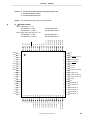 29
29
-
 30
30
-
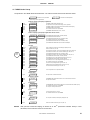 31
31
-
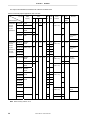 32
32
-
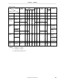 33
33
-
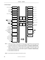 34
34
-
 35
35
-
 36
36
-
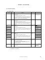 37
37
-
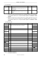 38
38
-
 39
39
-
 40
40
-
 41
41
-
 42
42
-
 43
43
-
 44
44
-
 45
45
-
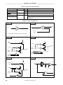 46
46
-
 47
47
-
 48
48
-
 49
49
-
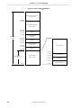 50
50
-
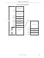 51
51
-
 52
52
-
 53
53
-
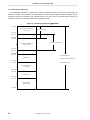 54
54
-
 55
55
-
 56
56
-
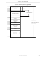 57
57
-
 58
58
-
 59
59
-
 60
60
-
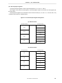 61
61
-
 62
62
-
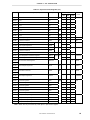 63
63
-
 64
64
-
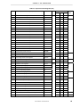 65
65
-
 66
66
-
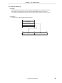 67
67
-
 68
68
-
 69
69
-
 70
70
-
 71
71
-
 72
72
-
 73
73
-
 74
74
-
 75
75
-
 76
76
-
 77
77
-
 78
78
-
 79
79
-
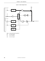 80
80
-
 81
81
-
 82
82
-
 83
83
-
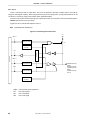 84
84
-
 85
85
-
 86
86
-
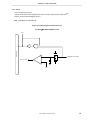 87
87
-
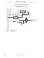 88
88
-
 89
89
-
 90
90
-
 91
91
-
 92
92
-
 93
93
-
 94
94
-
 95
95
-
 96
96
-
 97
97
-
 98
98
-
 99
99
-
 100
100
-
 101
101
-
 102
102
-
 103
103
-
 104
104
-
 105
105
-
 106
106
-
 107
107
-
 108
108
-
 109
109
-
 110
110
-
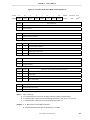 111
111
-
 112
112
-
 113
113
-
 114
114
-
 115
115
-
 116
116
-
 117
117
-
 118
118
-
 119
119
-
 120
120
-
 121
121
-
 122
122
-
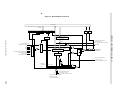 123
123
-
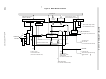 124
124
-
 125
125
-
 126
126
-
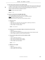 127
127
-
 128
128
-
 129
129
-
 130
130
-
 131
131
-
 132
132
-
 133
133
-
 134
134
-
 135
135
-
 136
136
-
 137
137
-
 138
138
-
 139
139
-
 140
140
-
 141
141
-
 142
142
-
 143
143
-
 144
144
-
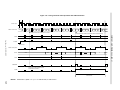 145
145
-
 146
146
-
 147
147
-
 148
148
-
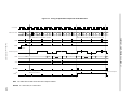 149
149
-
 150
150
-
 151
151
-
 152
152
-
 153
153
-
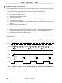 154
154
-
 155
155
-
 156
156
-
 157
157
-
 158
158
-
 159
159
-
 160
160
-
 161
161
-
 162
162
-
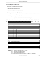 163
163
-
 164
164
-
 165
165
-
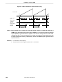 166
166
-
 167
167
-
 168
168
-
 169
169
-
 170
170
-
 171
171
-
 172
172
-
 173
173
-
 174
174
-
 175
175
-
 176
176
-
 177
177
-
 178
178
-
 179
179
-
 180
180
-
 181
181
-
 182
182
-
 183
183
-
 184
184
-
 185
185
-
 186
186
-
 187
187
-
 188
188
-
 189
189
-
 190
190
-
 191
191
-
 192
192
-
 193
193
-
 194
194
-
 195
195
-
 196
196
-
 197
197
-
 198
198
-
 199
199
-
 200
200
-
 201
201
-
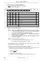 202
202
-
 203
203
-
 204
204
-
 205
205
-
 206
206
-
 207
207
-
 208
208
-
 209
209
-
 210
210
-
 211
211
-
 212
212
-
 213
213
-
 214
214
-
 215
215
-
 216
216
-
 217
217
-
 218
218
-
 219
219
-
 220
220
-
 221
221
-
 222
222
-
 223
223
-
 224
224
-
 225
225
-
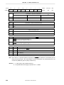 226
226
-
 227
227
-
 228
228
-
 229
229
-
 230
230
-
 231
231
-
 232
232
-
 233
233
-
 234
234
-
 235
235
-
 236
236
-
 237
237
-
 238
238
-
 239
239
-
 240
240
-
 241
241
-
 242
242
-
 243
243
-
 244
244
-
 245
245
-
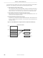 246
246
-
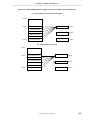 247
247
-
 248
248
-
 249
249
-
 250
250
-
 251
251
-
 252
252
-
 253
253
-
 254
254
-
 255
255
-
 256
256
-
 257
257
-
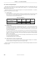 258
258
-
 259
259
-
 260
260
-
 261
261
-
 262
262
-
 263
263
-
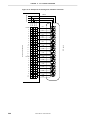 264
264
-
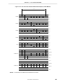 265
265
-
 266
266
-
 267
267
-
 268
268
-
 269
269
-
 270
270
-
 271
271
-
 272
272
-
 273
273
-
 274
274
-
 275
275
-
 276
276
-
 277
277
-
 278
278
-
 279
279
-
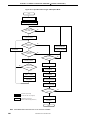 280
280
-
 281
281
-
 282
282
-
 283
283
-
 284
284
-
 285
285
-
 286
286
-
 287
287
-
 288
288
-
 289
289
-
 290
290
-
 291
291
-
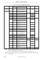 292
292
-
 293
293
-
 294
294
-
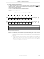 295
295
-
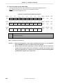 296
296
-
 297
297
-
 298
298
-
 299
299
-
 300
300
-
 301
301
-
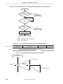 302
302
-
 303
303
-
 304
304
-
 305
305
-
 306
306
-
 307
307
-
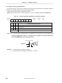 308
308
-
 309
309
-
 310
310
-
 311
311
-
 312
312
-
 313
313
-
 314
314
-
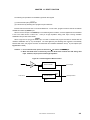 315
315
-
 316
316
-
 317
317
-
 318
318
-
 319
319
-
 320
320
-
 321
321
-
 322
322
-
 323
323
-
 324
324
-
 325
325
-
 326
326
-
 327
327
-
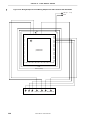 328
328
-
 329
329
-
 330
330
-
 331
331
-
 332
332
-
 333
333
-
 334
334
-
 335
335
-
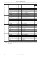 336
336
-
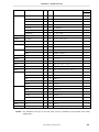 337
337
-
 338
338
-
 339
339
-
 340
340
-
 341
341
-
 342
342
-
 343
343
-
 344
344
-
 345
345
-
 346
346
-
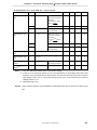 347
347
-
 348
348
-
 349
349
-
 350
350
-
 351
351
-
 352
352
-
 353
353
-
 354
354
-
 355
355
-
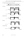 356
356
-
 357
357
-
 358
358
-
 359
359
-
 360
360
-
 361
361
-
 362
362
-
 363
363
-
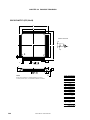 364
364
-
 365
365
-
 366
366
-
 367
367
-
 368
368
-
 369
369
-
 370
370
-
 371
371
-
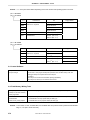 372
372
-
 373
373
-
 374
374
-
 375
375
-
 376
376
-
 377
377
-
 378
378
-
 379
379
-
 380
380
-
 381
381
-
 382
382
-
 383
383
-
 384
384
-
 385
385
-
 386
386
-
 387
387
-
 388
388


NEC PD78F9488 User manual
- Type
- User manual
- This manual is also suitable for
Ask a question and I''ll find the answer in the document
Finding information in a document is now easier with AI
Related papers
Other documents
-
Fujitsu F202RA User manual
-
Yamaha dx7/9 User manual
-
 Auvon 3-IN-1 TENS+EMS+Massage Device Quick start guide
-
evertz 5010‑VITC User manual
-
-
 Wolverine 8000 User manual
-
-
PARADOX TM50 Touch Quick Install Manual
-
Microsemi FlashPro Lite Quick Start Card
-
Renesas Answering Machine g1a User manual

