Page is loading ...

REJ10J0917-0100
Rev. 1.0
Issued : Dec 15, 2006
PRELIMINARY
Notice This is not a final specification.
Some parametric limits are subject to change.
32
Renesas 32-Bit RISC Microcomputers
SuperH
TM
RISC engine Family / SH7149 Group
M3
A
-HS49
SH7149 CPU Board
User's Manual

Microsoft, MS-DOS, Windows and Windows.NET are registered trademarks of Microsoft Corporation of the U.S. in the U.S.
and other countries.
IBM and AT are registered trademarks of International Business Machines Corporation of the U.S.
Adobe and Acrobat are registered trademarks of Adobe Systems Incorporated.
All other brand names and product names are registered trademarks or trademarks of the respective proprietors.
• Renesas is constantly making efforts to improve the quality and reliability of its products. However, not
all semiconductor products are trouble-free, they may become faulty or operate erratically. To ensure
that no accidents such as injury or a fire or no social damage may arise from Renesas semiconductor
products should they become faulty or operate erratically, please pay careful attention to the safety
design of your system by, for example, considering redundancy design and incorporating measures to
check the spread of a fire and prevent device malfunction.
• This manual only provides reference information to help customers purchase the appropriate type of
Renesas Technology product that suits the intended purpose of use, and the technical information
contained herein does not implicitly or otherwise grant a license or rights to use the intellectual property or
other rights of Renesas Technology.
• Renesas Technology will not assume any responsibility for damage or losses or infringement on the third
parties’ rights arising from the use of product data, diagrams, tables, programs, algorithms or example
application circuits presented in this manual.
• The product data, diagrams, tables, programs, algorithms and all other information presented herein reflect
the latest that was available at the time this manual was issued, and Renesas Technology reserves the
right to change the products or specifications described herein without prior notice. When purchasing
Renesas Technology semiconductor products, please contact Renesas Technology or Renesas
Technology Sales or other distributors to obtain the latest information, and also keep abreast of the
information published at the Renesas Technology home page (http://www.renesas.com) or through other
media.
• The information contained herein was carefully prepared and is believed to be correct. However, Renesas
Technology will not assume responsibility for losses that the customers by any possibility may suffer
because of erroneous description in this manual.
• To use the technical contents in product data, diagrams or tables or the programs or algorithms presented
herein for your system, please carefully evaluate their suitability as part of the entire system, not singly as
a technical content, program or algorithm alone, to determine in advance whether they are actually
suitable for your system. Renesas Technology will not assume responsibility for the suitability of said items
in user systems.
• The products presented herein are not designed or manufactured for use in equipment or systems that are
used under conditions where human life is concerned. If you plan to use the products presented herein for
special applications such as transportation, mobile, medical, aerospace, nuclear control or submarine
repeater equipment or systems, please consult Renesas Technology or Renesas Technology Sales or
other distributors.
• This manual may not be copied or reproduced, in whole or part, without prior written consent of Renesas
Technology.
• For more detailed information or for questions or doubts about this manual, please consult Renesas
Technology or Renesas Technology Sales or other distributors.
Requests for Safety Design
Precautions on Using This Manual

Revision History SH7149 CPU Board M3A-HS49User's Manual
Rev. Date of Issue Content of Revision
Page Page
1.0 Dec 15, 2006 - First edition issued

Table of Contents
Chapter 1 Overview.............................................................................................................................1-1
1.1 Overview ....................................................................................................................................................................1-2
1.2 Configuration..............................................................................................................................................................1-2
1.3 External Specifications...............................................................................................................................................1-3
1.4 External View .............................................................................................................................................................1-4
1.5 M3A-HS49 Block Diagram.......................................................................................................................................... 1-5
1.6 M3A-HS49 Board Overview .......................................................................................................................................1-6
1.7 M3A-HS49 Memory Mapping.....................................................................................................................................1-8
1.8 Absolute Maximum Ratings......................................................................................................................................1-11
1.9 Recommended Operating Conditions ...................................................................................................................... 1-11
Chapter2 Functional Overview ............................................................................................................2-1
2.1 Functional Overview...................................................................................................................................................2-2
2.2 CPU............................................................................................................................................................................2-3
2.3 Serial Port Interface.................................................................................................................................................... 2-4
2.4 I/O Ports.....................................................................................................................................................................2-5
2.5 Clock Module..............................................................................................................................................................2-7
2.6 Reset Module............................................................................................................................................................. 2-8
2.7 Interrupt Switches....................................................................................................................................................... 2-9
2.8 E10A-USB Interface.................................................................................................................................................2-10
Chapter3 Operational Specifications...................................................................................................3-1
3.1 M3A-HS49 Connectors Outline.................................................................................................................................. 3-2
3.1.1 H-UDI Connector (J1, J2)..................................................................................................................................3-3
3.1.2 Serial Port Connector (J3).................................................................................................................................3-5
3.1.3 External Power Supply Connectors (J4)............................................................................................................3-6
3.1.4 Power Supply Connector (J5) ........................................................................................................................... 3-7
3.1.5 User I/O Connector (J6-J8)...............................................................................................................................3-8
3.1.6 Extension Connectors (J9-J13)....................................................................................................................... 3-10
3.1.7 Extension Connector (J14)..............................................................................................................................3-14
3.2 Outline of Switches and LEDs.................................................................................................................................. 3-15
3.2.1 SH7149 Power Supply Select Jumper (JP1)................................................................................................... 3-16
3.2.2 FWE Pin Select Jumper (JP2).........................................................................................................................3-17
3.2.3 Serial Port Select Jumpers (JP3,JP4)............................................................................................................. 3-18
3.2.4 Switch and LED Functions.............................................................................................................................. 3-19
3.3 Package Dimensions of M3A-HS49.........................................................................................................................3-21
Appendix..............................................................................................................................................A-1
M3A-HS49 SCHEMATICS
(i)
Rev. 1.0 Dec 15, 2006
REJ10J0917-0100


Overview
1.1 Overview
Rev.1.0 Dec 15, 2006 1-2
REJ10J0917-0100
1
1.1 Overview
The M3A-HS49 is the CPU board designed for users to evaluate the functionality and performance of the SH7149
group of Renesas Technology original microcomputers, as well as develop and evaluate the application software for
this group of microcomputers. The SH7149's data bus, address bus and various internal peripheral circuit function
pins are connected to the extension connector of the M3A-HS49, allowing users to evaluate the timing relationship
with peripheral devices using measurement instruments or develop extension boards tailored to suit development
purposes. Furthermore, the E10A-USB or the on-chip emulator made by Renesas Technology can also be connected
to the M3A-HS49.
1.2 Configuration
Figure1.2.1 shows an example of system configuration using the M3A-HS49.
SH7149
SH7149 CPU Board
M3A-HS49
Extension
Board
USB
High-performance
Embeded Workshop(HEW)
Host
Computer
E10A-USB
H-UDI connector
(14-pin or 36-pin)
HEW
debugger
Serial port
connector
SuperH RISC engine
C/C++ compiler package
5V DC
Power Supply
(1.5
A min.)
* : It is necessary to buy separately for software development.
*
*
*
*
Can be created according
to applications
Extension
connector
*
Figure1.2.1 Example System Configuration of the M3A-HS49

Overview
1.3 External Specifications
Rev.1.0 Dec 15, 2006 1-3
REJ10J0917-0100
1
1.3 External Specifications
Table1.3.1 lists external specifications of M3A-HS49.
Table1.3.1 External Specifications of M3A-HS49
No. Item Content
1 CPU
SH7149
• Input(XIN) clock : 10MHz
• Bus clock : 40MHz, max
• CPU clock : 80MHz, max
• On-chip memory
Flash memory : 256KB
RAM : 8KB
2 Connectors
• Extension connector (Bus, I/O, VCC, GND)
• User I/O connector (SH7149’s MTU2, A/D function pins)
• Serial Port connector (D-sub 9pins)
• H-UDI connector (36pins)
• H-UDI connector (14pins)
3 LED
• POWER LED (1pc.)
• LED for Interrupt confirmation (1pc.)
• User LED (6pcs.)
4 Switches
• Reset switch (1pc.)
• NMI switch (1pc.)
• MRES switch (1pc.)
• IRQ0 switch (1pc.)
• DIP switch for System setting (1pc.,3 poles)
• DIP switch for users (1pc.,4 poles)
5 External dimensions
• Dimensions : 100mm x 100mm
• Mounting form : 4-layer, double-side mounted
• Board configuration : 1 board


Overview
1.5 M3A-HS49 Block Diagram
Rev.1.0 Dec 15, 2006 1-5
REJ10J0917-0100
1
1.5 M3A-HS49 Block Diagram
Figure1.5.1 shows the system block diagram of M3A-HS49.
Extension connector
Serial Port
Connector
SH7149
(80MHz)
SH7149 CPU Board
M3A-HS49
Bus clock: 40MHz
16
H-UDI
H-UDI Connector
(36-pin)
AUD
H-UDI Connector
(14-pin)
User I/O
Conn
ector
Figure1.5.1 System Block Diagram of M3A-HS49

Overview
1.6 M3A-HS49 Board Overview
Rev.1.0 Dec 15, 2006 1-6
REJ10J0917-0100
1
1.6 M3A-HS49 Board Overview
Figure1.6.1 shows the M3A-HS49 board overview.
<Top view of the component side >
U1
SH7149
SW1
Power Switch
LED1
Power LED
J5
Power Supply
Connector
J1
H-UDI Connector
(36-pin)
J2
H-UDI Connector
(14-pin)
SW5
NMI
Switch
SW7
MRES
Switch
SW6
IRQ0
Switch
SW2
RESET
Switch
SW3
DIP Switch
for users
J3
Serial Port
Connector
SW4
DIP Switch
for system setting
LED2 to 7
User LED
LED8
Interrupt Confirmation
J14
Extension
Connector
*
U3
Reset IC
J7,J8
User I/O Connector
U2
RS-232C Driver
*
JP1
Power
SupplySelect
Jumpers
JP2
FWE Pin
Select
Jumpers
JP3,JP4
Serial Port
Select
Jumpers
<Top view of the solder side >
J13
Extension Connector
J6
User I/O Connector
J12
Extension Connector
J10
Extension Connector
J9
Extension Connector
J11
Extension Connector
*
*
*
*
*
*
Note *: Not mounted
Figure1.6.1 M3A-HS49 Board Overview

Overview
1.6 M3A-HS49 Board Overview
Rev.1.0 Dec 15, 2006 1-7
REJ10J0917-0100
1
Table1.6.1 lists main components mounted in M3A-HS49.
Table1.6.1 Main Components Mounted in M3A-HS49
Symbol Parts Name Remarks Parts number for
recommended components
that are not mounted
U1 CPU SH7149 (Renesas)
U1 CPU Socket
U2 RS-232C Driver
U3 Reset IC M51957BFP (Renesas)
U4 Logic IC
X1 Oscillator 10.00MHz
J1 H-UDI Connector 36-pin type
J2 H-UDI Connector 14-pin type
J3 Serial Port Connector
J4 External Power Supply Connector Not mounted A2-2PA-2.54DSA (Hirose)
J5 Power Supply Connector
J6 User I/O Connector Not mounted
XG4C-2634 (Omron)
J7,J8 User I/O Connector Not mounted
A2-3PA-2.54DSA (Hirose)
J9,J11,J12 Extension Connector Not mounted
XG4C-2031 (Omron)
J10,J13 Extension Connector Not mounted
XG4C-4031 (Omron)
J14 Extension Connector Not mounted
3428-6002LCSC
(Sumitomo 3M)
LED1 Power LED Blue
LED2 to 7 User LED Green
LED8
LED for Interrupt confirmation
Red/Yellowgreen
(Two colors)
SW1 Power Switch
SW2 Reset Switch
SW3 DIP Switch for users
SW4 DIP Switch for system setting
SW5 NMI Switch
SW6 IRQ0 Switch
SW7 MRES Switch

Overview
1.7 M3A-HS49 Memory Mapping
Rev.1.0 Dec 15, 2006 1-8
REJ10J0917-0100
1
1.7 M3A-HS49 Memory Mapping
Figure1.7.1, Figure1.7.2 and Figure1.7.3 show a memory mapping example of SH7149 in the M3A-HS49.
On-chip ROM(256KB)
Reserved
Logical space of the SH7149
MCU mode 3
(Single Chip mode)
On-chip RAM(8KB)
On-chip Peripheral Module
H’0000 0000
H’FFFF 8FFF
H’FFFF 9000
H’FFFF AFFF
H’FFFF B000
H’FFFF BFFF
H’FFFF C000
H’FFFF FFFF
Memory Mapping
of the M3A-HS49
Reserved
On-chip RAM(8KB)
On-chip Peripheral Module
Reserved
Reserved
H’FFFF 8FFF
H’FFFF 9000
H’FFFF AFFF
H’FFFF B000
H’FFFF BFFF
H’FFFF C000
H’F
FFF FFFF
H’0003 FFFF
H’0004 0000
H’0000 0000
H’0003 FFFF
H’0004 0000
On-chip ROM(256KB)
Figure1.7.1 Memory Mapping Example of SH7149 (MCU mode 3)

Overview
1.7 M3A-HS49 Memory Mapping
Rev.1.0 Dec 15, 2006 1-9
REJ10J0917-0100
1
CS0 space:64MB
CS1 space:64MB
Reserved
Logical space of the SH7149
MCU mode 0,1
(On-chip ROM disabled mode)
On-chip RAM(8KB)
On-chip Peripheral Module
H’0000 0000
H’03FF FFFF
H’0400 0000
H’07FF FFFF
H’0800 0000
H’FFFF 8FFF
H’FFFF 9000
H’FFFF AFFF
H’FFFF B000
H’FFFF BFFF
H’FFFF C000
H’FFFF FFFF
User Area
*
User Area
*
Memory Mapping
of the M3A-HS49
予約領域
(使用禁止)
Reserved
On-chip RAM(8KB)
On-chip Peripheral Module
H’0000 0000
Reserved
Reserved
H’03FF FFFF
H’0400 0000
H’07FF FFFF
H’0800 0000
H’FFFF 8FFF
H’FFFF 9000
H’FFFF AFFF
H’FFFF B000
H’FFFF BFFF
H’FFFF C000
H’FFFF FFFF
[Note]
*
:Because the address pins of SH7149 are A19 to A0, the address space that can be actually used is 1MB.
Figure1.7.2 Memory Mapping Example of SH7149 (MCU mode 0,1)

Overview
1.7 M3A-HS49 Memory Mapping
Rev.1.0 Dec 15, 2006 1-10
REJ10J0917-0100
1
On-chip ROM(256KB)
CS1 space:64MB
Reserved
Logical space of the SH7149
MCU mode 2
(On-chip ROM enabled mode)
On-chip RAM(8KB)
On-chip Peripheral Module
H’0000 0000
H’03FF FFFF
H’0400 0000
H’07FF FFFF
H’0800 0000
H’FFFF 8FFF
H’FFFF 9000
H’FFFF AFFF
H’FFFF B000
H’FFFF BFFF
H’FFFF C000
H’FFFF FFFF
Memory Mapping
of the M3A-HS49
Reserved
On-chip RAM(8KB)
On-chip Peripheral Module
Reserved
Reserved
H’FFFF 8FFF
H’FFFF 9000
H’FFFF AFFF
H’FFFF B000
H’FFFF BFFF
H’FFFF C000
H’FFFF FFFF
CS0 space:64MB
H’0003 FFFF
H’0004 0000
H’01FF FFFF
H’0200 0000
Reserved
H’0000 0000
H’03FF FFFF
H’0400 0000
H’07FF FFFF
H’0800 0000
H’0003 FFFF
H’0004 0000
H’01FF FFFF
H’0200 0000
On-chip ROM(256KB)
User Area
*
User Area
*
Reserved
[Note]
*
:Because the address pins of SH7149 are A19 to A0, the address space that can be actually used is 1MB.
Figure1.7.3 Memory Mapping Example of SH7149 (MCU mode 2)

Overview
1.8 Absolute Maximum Ratings
Rev.1.0 Dec 15, 2006 1-11
REJ10J0917-0100
1
1.8 Absolute Maximum Ratings
Table1.8.1 lists the absolute maximum ratings of M3A-HS49.
Table1.8.1 Absolute Maximum Ratings of M3A-HS49
Symbol Parameter Rated Value Remarks
VCC 5V System Power Supply Voltage -0.3V to 6.0V Relative to VSS
Topr Operating Ambient Temperature 0°C to 50°C No dewdrops allowed.
Use in corrosive gas environment prohibited.
Tstr Storage Ambient Temperature -10°C to 60°C No dewdrops allowed.
Use in corrosive gas environment prohibited.
Note: The ambient temperature refers to the air temperature in places closest possible to the board.
1.9 Recommended Operating Conditions
Table1.9.1 lists recommended operating conditions of M3A-HS49.
Table1.9.1 Recommended Operating Conditions of M3A-HS49
Symbol Parameter Rated Value Remarks
VCC 5V System Power Supply Voltage 4.75V to 5.25V Relative to VSS
— Maximum Current Consumption in the Board Within 1A
Topr Operating Ambient Temperature 0°C to 50°C No dewdrops allowed.
Use in corrosive gas environment prohibited.

Overview
1.8 Absolute Maximum Ratings
Rev.1.0 Dec 15, 2006 1-12
REJ10J0917-0100
1
* This is a blank page *


Functional Overview
2.1 Functional Overview
Rev.1.0 Dec 15, 2006 2-2
REJ10J0917-0100
2
2.1 Functional Overview
The M3A-HS49 is the SH7149 CPU board that has functions listed in
Table2.1.1.
Table2.1.1 lists functional modules of M3A-HS49.
Table2.1.1 Functional Modules of M3A-HS49
Section Function Content
2.2 CPU
SH7149
• Input(XIN) clock : 10MHz
• Bus clock : 40MHz, max
• CPU clock : 80MHz, max
• On-chip Memory
- Flash memory : 256KB
- RAM : 8KB
2.3 Serial Port Interface Connects SCI1 of the SH7149 to the Serial Port connector
2.4 Input/Output Ports Connects to the I/O ports of the SH7149
2.5 Clock Module Controls the system clock
2.6 Reset Module Controls device reset accommodated by the M3A-HS49
2.7 Interrupt Switches Controls interrupt (NMI,IRQ0,MRES)
2.8 E10A-USB Interface SH7149 H-UDI/AUD interface
- Operational specifications Connectors, switches and LEDs
• SH7149 extension connector
• Switches and LEDs
• H-UDI connector
Detailed in Chapter 3.

Functional Overview
2.2 CPU
Rev.1.0 Dec 15, 2006 2-3
REJ10J0917-0100
2
2.2 CPU
The M3A-HS49 contains the 32-bit RISC microcomputer SH7149 that operates with a maximum 80MHz of CPU
clock frequency. The SH7149 includes 256-Kbyte flash memory, and 8-Kbyte SRAM, making it useful in a wide range
of applications from data processing to equipment control.
The M3A-HS49 can be operated with a maximum 80MHz of CPU clock frequency (external bus 40MHz, max) using
a 10MHz input clock.
Figure2.2.1 shows the block diagram of SH7149 in the M3A-HS49.
EXTAL
XTAL
PA15/CK
MD1
MD0
FWE
WDTOVF
RES
Clock
Mode
System
Control
NMI
NMI switch
PF0/AN0
PF2/AN2
PF4/AN4
PF6/AN6
PF8/AN8
PF9/AN9
PF10/AN10
PF11/AN11
PF12/AN12
PF13/AN13
PF14/AN14
PF15/AN15
A/D
Converter
SH7149
PA0/A0
PA1/A1
PA2/A2
PA3/A3
PA4/A4
PA5/A5
PA10/A6
PA11/A7
PA12/A8
PA13/A9
PA14/A10
PE4/A11
PE5/A12
PE6/A13
PE7/A14
PE8/A15
PB2/A16
PB3/A17
PB4/A18
PB5/A19
Address bus
PD0/D0
PD1/D1
PD2/D2
PD3/D3
PD4/D4
PD5/D5
PD6/D6
PD7/D7
PD8/D8
PD9/D9
PD10/D10
PD11/D11
PD12/D12
PD13/D13
PD14/D14
PD15/D15
Data bus
PE10/CS0
PA6/RD
PA7/WRH
PA8/WRL
PA9/WAIT
Bus
Control
PE0
PE9
PE11
PE12
PE14
PE15
User
LED
PB0
PB16
PB17
PB18
User DIP Switch
PB1/BREQ/TIC5W
PE3/TIOC0D/SCK0
PE2/TIOC0C/TXD0
PE1/TIOC0B/RXD0
GPIO/SCI/
MTU2
RXD1
TXD1
Serial Port
Connector
AUDATA0
H-UDI
Connector
IRQ0
IRQ0 Switch
AUDATA1
AUDATA2
AUDATA3
H-UDI
Connector
AUDCK
AUDSYNC
PE19/TDO
PE18/TDI
PE17/TCK
PE16/ASEBRKAK/ASEBRK
ASEMD0
PE21/TRST
PE20/TMS
H-UDI
Connector
MRES switch
PE13/MRES
Figure2.2.1 Block Diagram of SH7149

Functional Overview
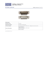
2.3 Serial Port Interface
Rev.1.0 Dec 15, 2006 2-4
REJ10J0917-0100
2
2.3 Serial Port Interface
The SH7149 included in the M3A-HS49 contains a UART module. In the M3A-HS49, SCI channel 1 is connected to
J3 (Serial Port connector). Switch the connection of the J3 connector and J14 connector by the jumper (JP3, JP4)
setting.
Figure2.3.1 shows the block diagram of serial port interface in the M3A-HS49.
SH7149
RXD1(PA3)
TXD1(PA4)
DCD
RxD
TxD
DTR
GND
DSR
RTS
CTS
RI
1
2
3
4
5
6
7
8
9
NC
GND
NC
Serial Port
Connector (J3)
RS232C
Driver
Extension Connector (J14)
RXD1(PA3)
TXD1(PA4)
1
2
3
1
2
3
JP4
JP3
Figure2.3.1 Block Diagram of Serial Port Interface
/