
UM10267
PCA9698 demonstration board OM6281
Rev. 01 — 24 September 2008 User manual
Document information
Info Content
Keywords I2C, PCA9698, GPIO
Abstract The OM6281 is an add-on to NXP’s I
2
C 2005-1 demo board. This
daughter board makes it easy to test and design with the PCA9698, a
Fast-mode Plus (Fm+) 40-bit GPIO device. These boards, along with the
I2CUSB Lite GUI (PC based), provide an easy to use evaluation platform.

UM10267_1 © NXP B.V. 2008. All rights reserved.
User manual Rev. 01 — 24 September 2008 2 of 16
Contact information
For more information, please visit: http://www.nxp.com
For sales office addresses, please send an email to: [email protected]
NXP Semiconductors
UM10267
PCA9698 demonstration board OM6281
Revision history
Rev Date Description
01 20080924 Initial release

UM10267_1 © NXP B.V. 2008. All rights reserved.
User manual Rev. 01 — 24 September 2008 3 of 16
NXP Semiconductors
UM10267
PCA9698 demonstration board OM6281
1. Introduction
The PCA9698 evaluation features headers to access all GPIO bits and LEDs for GPIO
(output) demonstration. In addition, a PCA9530 LED dimmer/blinker is on-board to
demonstrate the capability of generating a complex dimming/blinking pattern
simultaneously on 40 LEDs. The board can be connected is series with other I
2
C-bus
demo-boards to create an evaluation system.
The IC communicates to the host via the industry standard I
2
C-bus/SMBus port. The
evaluation software runs under MS Windows PC platform.
2. Features
• A complete evaluation platform for the PCA9698 40-bit GPIO
• Easy to use GUI-based software demonstrates the capabilities of the PCA9698
• On-board LEDs for visual experience
• Convenient test points for easy scope measurements and GPIO access
• USB interface to the host PC
• No external power supply required
3. Getting started
3.1 Assumptions
Familiarity with the I
2
C-bus is helpful but not required.
3.2 Static handling requirements
3.3 Minimum system requirements
•
PC Pentium 60 processor (or equivalent), 8 MB RAM, 10 MB of hard drive space
• One USB port (either 2.0 or 1.1 compatible)
• Windows 98SE, ME, 2000, XP, or Vista
• I
2
C 2005-1 Demonstration board (OM6275)
3.4 Power requirements
The NXP Semiconductors I
2
C Demonstration Board 2005-1 and OM6281 hardware
obtain power from the PC USB port. Care should be taken not to exceed the USB port
current capabilities.
CAUTION
This device is sensitive to ElectroStatic Discharge (ESD). Therefore care should be taken
during transport and handling. You must use a ground strap or touch the PC case or other
grounded source before unpacking or handling the hardware.

UM10267_1 © NXP B.V. 2008. All rights reserved.
User manual Rev. 01 — 24 September 2008 4 of 16
NXP Semiconductors
UM10267
PCA9698 demonstration board OM6281
4. Installation
4.1 I
2
C 2005-1 board and WIN-12CUSB Lite software
The OM6281 is a daughter card to the OM6275 I2C2005-1 demo board.
You may download the WIN-I2CUSB Lite Software, the OM6275 user manual UM10206,
and find ordering information at the NXP web site
www.standardics.nxp.com/support/boards/
.
4.2 OM6281 connection to I
2
C 2005-1 board
The I
2
C 2005-1 board should be disconnected from your PC. The OM6281 board has a
9-pin female connector that allows the demo board to mount directly onto the I
2
C 2005-1
board at the JP1 location.
Connect the OM6281 board to the I
2
C 2005-1 board before connecting the USB cable.
Once the board is connected, connect the USB cable and start the WIN-I2CUSB Lite
software. You are now ready to evaluate the PCA9698.

UM10267_1 © NXP B.V. 2008. All rights reserved.
User manual Rev. 01 — 24 September 2008 5 of 16
NXP Semiconductors
UM10267
PCA9698 demonstration board OM6281
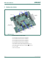
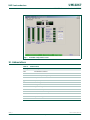
5. Hardware description
The OM6281 board has 8 jumper headers.
• Port0: Headers for port 0 I/O bits 0.0 through 0.7
• Port1: Headers for port 1 I/O bits 1.0 through 1.7
• Port2: Headers for port 2 I/O bits 2.0 through 2.7
• Port3: Headers for port 3 I/O bits 3.0 through 3.7
• Port4: Headers for port 4 I/O bits 4.0 through 4.7
• AD0: Address selector header. Default is AD0 HIGH (2-3)
• OE_Select: Output enable selector. Default is OE LOW (5-6)
• 5V: V
CC
header
• GND: Ground header
Fig 1. OM6281 demo board
address select
port headers
SCL SDA
card extender
connector
INT LED
PCA9698
OE select
PCA9530
9-pin connector
to I2C 2005-1 board

xxxx xxxxxxxxxxxxxxxxxxxxxxxxxxxxxx x xxxxxxxxxxxxxx xxxxxxxxxx xxx xxxxxx xxxxxxxxxxxxxxxxxxxxxxx xxxxxxxxxxxxxxxxxxxxxx
xxxxx xxxxxx xx xxxxxxxxxxxxxxxxxxxxxxxxxxxxx xxxxxxxxxxxxxxxxxxxxxx xxxxxxxxxxx xxxxxxx xxxxxxxxxxxxxxxxxxx
xxxxxxxxxxxxxxxx xxxxxxxxxxxxxx xxxxxx xx xxxxxxxxxxxxxxxxxxxxxxxxxxxxxxxx xxxxxxxxxxxxxxxxxxxxxxxx xxxxxxx
xxxxxxxxxxxxxxxxxxxxxxxxxxxxxxxxxxxxxxxxxxxxxx xxxxxxxxxxx xxxxx x x
UM10267_1 © NXP B.V. 2008. All rights reserved.
User manual Rev. 01 — 24 September 2008 6 of 16
NXP Semiconductors
UM10267
PCA9698 demonstration board OM6281
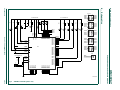
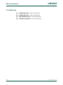
6. Schematics
Fig 2. OM6281 schematic (part 1 of 2)
IO0.1
IO0.3
IO0.5
IO0.7
Port 0
IO0.0
IO0.2
IO0.4
IO0.6
IO1.1
IO1.3
IO1.5
IO1.7
Port 1
IO1.0
IO1.2
IO1.4
IO1.6
IO2.1
IO2.3
IO2.5
IO2.7
Port 2
IO2.0
IO2.2
IO2.4
IO2.6
IO3.1
IO3.3
IO3.5
IO3.7
Port 3
IO3.0
IO3.2
IO3.4
IO3.6
IO4.1
IO4.3
IO4.5
IO4.7
Port 4
IO4.0
IO4.2
IO4.4
IO4.6
1
3
5
7
2
4
6
8
1
3
5
7
2
4
6
8
1
3
5
7
2
4
6
8
1
3
5
7
2
4
6
8
1
3
5
7
2
4
6
8
1
2
JP3
GND
5 V unswitched
LED4
R9
LED3
R8
LED2
R7
LED6
R12
5 V unswitched
LED5
R11
LED1
R10
PIN13
PIN14
PIN15
PIN16
PIN17
PIN19
PIN20
PIN21
PIN22
PIN24
PIN25
PIN26
PIN31
PIN32
PIN33
PIN36
IO1.0
IO1.1
IO1.2
IO1.3
IO1.4
IO1.5
IO1.6
IO1.7
IO2.0
IO2.1
IO2.2
IO2.3
IO2.4
IO2.5
IO2.6
IO2.7
PIN37
PIN35
PIN38
PIN40
PIN41
PIN42
PIN43
PIN44
IO3.0
IO3.1
IO3.2
IO3.3
IO3.4
IO3.5
IO3.6
IO3.7
PIN54
PIN53
PIN52
PIN50
PIN49
PIN48
PIN47
PIN45
IO4.7
IO4.6
IO4.5
IO4.4
IO4.3
IO4.2
IO4.1
IO4.0
IO0.4
IO0.5
IO0.6
IO0.7
PIN3
PIN4
PIN5
PIN7
PIN8
PIN9
PIN10
PIN12
IO0.0
IO0.1
IO0.2
IO0.3
IO0.4
IO0.5
IO0.6
IO0.7
R14
R13
R15
LED0
LD1
R1
PIN18
VDD0
5 V unswitched
PIN46
VDD1
R2
GND
PWR
C1 C2
GND
R3
R4
R5
R6
1
2
JP2
2
1
JP1
INT
SDA
SCL
PIN1
PIN2
SDA
SCL
RESET
PIN56
RESET
OE
PIN30
OE
INT
PIN55
INT
IC1
GND
PIN51
PIN39
PIN34
PIN23
PIN11
PIN6
VSS5
VSS4
VSS3
VSS2
VSS1
VSS0
1
2
AD1
3
AD0
PIN27
AD2
PIN29
AD1
PIN28
5 V unswitched
R16
002aad33
9

xxxxxxxxxxxxxxxxxxxxx xxxxxxxxxxxxxxxxxxxxxxxxxx xxxxxxx x x x xxxxxxxxxxxxxxxxxxxxxxxxxxxxxx xxxxxxxxxxxxxxxxxxx xx xx xxxxx
xxxxxxxxxxxxxxxxxxxxxxxxxxx xxxxxxxxxxxxxxxxxxx xxxxxx xxxxxxxxxxxxxxxxxxxxxxxxxxxxxxxxxxx xxxxxxxxxxxx x x
xxxxxxxxxxxxxxxxxxxxx xxxxxxxxxxxxxxxxxxxxxxxxxxxxxx xxxxx xxxxxxxxxxxxxxxxxxxxxxxxxxxxxxxxxxxxxxxxxxxxxxxxxx xxxxxxxx
xxxxxxxxxxxxxxxxxxxxxxxxx xxxxxxxxxxxxxxxxxxxx xxx
UM10267_1 © NXP B.V. 2008. All rights reserved.
User manual Rev. 01 — 24 September 2008 7 of 16
NXP Semiconductors
UM10267
PCA9698 demonstration board OM6281
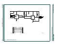
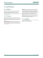
Fig 3. OM6281 schematic (part 2 of 2)
PIN1
PIN5RESET
PIN6
PIN7
5 V unswitched
R17
GND
LED10
6
4
2
SDA
SCL
RESET
A0
V
DD
GND
LED1
IC2
SDA
SCL
PIN2
LED0
PIN3
LED1
LED0
PIN4 PIN8
GND
C3
PS1
A
PS2
B
R18
LED9
GND
C4
IC3
V
CC
PS5
GND
GND
PS3
PS4
Y
BLNK_DIM
R19
74LVC1G38
GND
OE_SELECT
5
3
1
OE
5 V unswitched
002aad38
3
US7
5 V unswitched
5 V switched
3.3 V unswitched
3.3 V switched
SCL
GND
SDA
INPUT
OUTPUT
training board header
US2
5 V unswitched
5 V switched
3.3 V unswitched
3.3 V switched
SCL
GND
SDA
INPUT
OUTPUT
training board header

UM10267_1 © NXP B.V. 2008. All rights reserved.
User manual Rev. 01 — 24 September 2008 8 of 16
NXP Semiconductors
UM10267
PCA9698 demonstration board OM6281
7. OM6281 demonstration board main components
8. PCA9698 evaluation steps
The PCA9698 functions are controlled by WIN-I2CUSB Lite GUI. Refer to the PCA9698
data sheet for additional information on the registers and functionality.
8.1 Controlling LEDs using GPIO output
1. Connect the hardware as described in Section 4 “Installation”. The PCA9698 address
is set to 0x42.
2. Start the GUI software.
3. The main screen will appear.
4. From the ‘Device’ drop-down menus select ‘IO Expanders’ and from the subsequent
drop-down menu select ‘PCA9698 40-bit I/O Expander’.
5. The device configuration screen will be displayed as in Figure 4
.
6. Check the ‘Auto Write’ box on the right to send new register contents as soon as we
change them.
7. Select the Bank0 tab. The default configuration is shown as in Figure 5
.
8. To enable the outputs, click on the check box IOC0 in the ‘Configuration 0’ register to
enable the output on bit 0. An alternative is to write the hex value directly in the box.
9. The LED connected to Port0.0 is now on.
10. To turn it off, click on the OP0 box to set the output signal HIGH. Verify LED0 is off.
11. Additional LEDs are located at Portx.0 on banks 1-4. An RGB LED is located at
Port0.1 to Port0.3. Experiment by turning those LEDs on and off.
Table 1. OM6281 main components
Device Description Address Location
PCA9698DGG 40-bit Fm+ I
2
C-bus advanced I/O port with RESET,
OE, and INT
0x42 IC1
PCA9530DP 2-bit I
2
C-bus LED blinker/dimmer 0xC2 IC2
74LVC1G38 2-input NAND gate n/a IC3

UM10267_1 © NXP B.V. 2008. All rights reserved.
User manual Rev. 01 — 24 September 2008 9 of 16
NXP Semiconductors
UM10267
PCA9698 demonstration board OM6281
Fig 4. PCA9698 device configuration screen
Fig 5. Bank0 configuration

UM10267_1 © NXP B.V. 2008. All rights reserved.
User manual Rev. 01 — 24 September 2008 10 of 16
NXP Semiconductors
UM10267
PCA9698 demonstration board OM6281
8.2 GPIO input
8.2.1 Polling mode
In polling mode, the host controller must read the input port registers at predetermined
intervals to check if an input has changed. Depending on the application, the interrupt
mode described in Section 8.2.2
may be a more efficient method of verifying changes of
state on the input pins.
1. Select Bank0 and verify that the default values are displayed.
2. Since the PCA9698 has a small pull-up on the I/O, a read on the Input Port 0 register
returns 0xFF.
3. Pull Port0.7 to a logic LOW.
4. Read the Input Port 0 register and verify that the Input Port 0 register reads 0x7F.
8.2.2 Interrupt mode
In interrupt mode the interrupt pin is toggled to signal the host controller when an input
change of state has been detected. The interrupt mask register specifies which signal is
allowed to generate an interrupt.
1. Select Bank1 and verify the default values are active.
2. Un-check the MSK7 and MSK6 bits in the Mask Interrupt 1 register.
3. With the aid of an external pull-down, pull Port1.6 and Port1.7 bits to a logic LOW.
4. Verify the INT light is illuminated on the board.
5. Toggle the MSK6 and MSK7 bits and verify the INT light goes off only when both bits
are masked.
6. Read the Input Port 1 register and verify the contents is now 0x3F and the INT light is
off.
7. Pull the IO1.7 signal HIGH and verify that the interrupt light is on.
8. Toggle the MSK6 bit and verify that the INT light remains on.
9. Read the Input Port 1 register and verify that the contents is 0xBF and the INT light is
off.
9. Application specific: LED blinking and dimming with the PCA9530 and
the PCA9698
9.1 Theory of operation
The PCA9698 has the capability to drive up to 40 LEDs (within certain power restrictions
on the package, which can be overcome with the use of FETs). To enhance the
application of the PCA9698, a PCA9530 can be used to drive the Output Enable (OE
) pin
to blink and dim the output of the LEDs. A pattern with intermediate complexity can be
easily generated by combining the outputs of the PCA9530.
A 74LVC1G38GW NAND gate is used to demonstrate the OE
polarity inversion (active
HIGH instead of default active LOW) of the PCA9698.

UM10267_1 © NXP B.V. 2008. All rights reserved.
User manual Rev. 01 — 24 September 2008 11 of 16
NXP Semiconductors
UM10267
PCA9698 demonstration board OM6281
To drive LEDs, the GPIOs on the PCA9698 are configured to output mode. The LEDs are
turned on and off by driving the outputs LOW and HIGH. To blink and dim the LEDs, the
OE
pin is tied to the outputs of the PCA9530 through a NAND gate. When the OE is driven
HIGH, the outputs on the PCA9698 will be enabled. This will turn on the LEDs that are
connected to outputs driven LOW. The truth table in Table 2
illustrates the sequence.
Combining the blink and dimming, along with the individual on/off control of each LED
allows the user to create eye-catching display patterns. The example outlined in
Section 9.2
will demonstrate how to obtain the waveform shown in Figure 6.
Table 2. LED control truth table
LED0 LED1 OE GPIO output LED
0 0 1 LOW ON
0 1 1 LOW ON
1 0 1 LOW ON
110LOWOFF
Fig 6. Blinking and dimming pattern

UM10267_1 © NXP B.V. 2008. All rights reserved.
User manual Rev. 01 — 24 September 2008 12 of 16
NXP Semiconductors
UM10267
PCA9698 demonstration board OM6281
9.2 Blinking/dimming with the PCA9530 demonstration steps
The following exercise demonstrates how this is achieved.
1. Move the OE_Select jumper to the 3-4 position. The PCA9530 will now control the OE
pin.
2. Set-up the hardware and software as described in Section 4 “
Installation”.
3. Open the PCA9698 GUI.
4. In the ‘Device Configuration’ tab, select OE
enable HIGH.
5. Select the Bank0 tab.
6. Enable the output for bits 1-3. These bits control the RGB LED on the board.
7. The RGB LED should be off.
8. Go to the ‘Device’ selection tab and select the ‘LED blinkers and Dimmers’ to select
the PCA9530. The configuration screen will appear. See Figure 7
.
9. Select the ‘Auto-write’ option.
10. Slide the selection tab on LED0 to the ON position.
11. Verify the RBG LED is ON, displaying white.
12. Move the LED0 slider to PWM0.
13. Move the LED0 Period slider to 0.033 seconds and the LED0 Duty Cycle to 14.45 %.
14. Observe the pattern displayed on by the RGB LED.
15. Move the LED1 Period slider to 0.296 seconds and the LED1 Duty Cycle to 12.11 %.
16. Move the LED1 slider to PWM1.
17. Observe the pattern being output on the RGB LED.
18. Observe LED 8 and LED 9, which individual blink/dim patterns generated by the LED0
and LED1 outputs on the PCA9530.
19. To change the color displayed by the RGB LED, go back to the PCA9698 Bank0.
20. Turn off the green LED by selecting bit 2 HIGH.
21. Verify that the blink color is now mauve.
22. Turn off the red LED by selecting bit 1 HIGH.
23. Verify the blink color is now blue.
24. Slide the Period and Duty Cycle bars for the LED1 and LED0 and observe how the
blink and dim patterns vary.

UM10267_1 © NXP B.V. 2008. All rights reserved.
User manual Rev. 01 — 24 September 2008 13 of 16
NXP Semiconductors
UM10267
PCA9698 demonstration board OM6281
10. Abbreviations
Fig 7. PCA9530 configuration screen
Table 3. Abbreviations
Acronym Description
FET Field-Effect Transistor
Fm+ Fast-mode Plus
GPIO General Purpose Input/Output
GUI Graphical User Interface
I/O Input/Output
I
2
C-bus Inter Integrated Circuit bus
IC Integrated Circuit
LED Light-Emitting Diode
PC Personal Computer
RAM Random Access Memory
RGB Red/Green/Blue
SMBus System Management Bus
USB Universal Serial Bus

UM10267_1 © NXP B.V. 2008. All rights reserved.
User manual Rev. 01 — 24 September 2008 14 of 16
NXP Semiconductors
UM10267
PCA9698 demonstration board OM6281
11. References
[1] PCA9698 data sheet — NXP Semiconductors
[2] PCA9530 data sheet — NXP Semiconductors
[3] 74LVC1G38 data sheet — NXP Semiconductors
[4] I
2
C 2005-1 User Manual — NXP Semiconductors

UM10267_1 © NXP B.V. 2008. All rights reserved.
User manual Rev. 01 — 24 September 2008 15 of 16
NXP Semiconductors
UM10267
PCA9698 demonstration board OM6281
12. Legal information
12.1 Definitions
Draft — The document is a draft version only. The content is still under
internal review and subject to formal approval, which may result in
modifications or additions. NXP Semiconductors does not give any
representations or warranties as to the accuracy or completeness of
information included herein and shall have no liability for the consequences of
use of such information.
12.2 Disclaimers
General — Information in this document is believed to be accurate and
reliable. However, NXP Semiconductors does not give any representations or
warranties, expressed or implied, as to the accuracy or completeness of such
information and shall have no liability for the consequences of use of such
information.
Right to make changes — NXP Semiconductors reserves the right to make
changes to information published in this document, including without
limitation specifications and product descriptions, at any time and without
notice. This document supersedes and replaces all information supplied prior
to the publication hereof.
Suitability for use — NXP Semiconductors products are not designed,
authorized or warranted to be suitable for use in medical, military, aircraft,
space or life support equipment, nor in applications where failure or
malfunction of an NXP Semiconductors product can reasonably be expected
to result in personal injury, death or severe property or environmental
damage. NXP Semiconductors accepts no liability for inclusion and/or use of
NXP Semiconductors products in such equipment or applications and
therefore such inclusion and/or use is at the customer’s own risk.
Applications — Applications that are described herein for any of these
products are for illustrative purposes only. NXP Semiconductors makes no
representation or warranty that such applications will be suitable for the
specified use without further testing or modification.
12.3 Trademarks
Notice: All referenced brands, product names, service names and trademarks
are the property of their respective owners.
I
2
C-bus — logo is a trademark of NXP B.V.

NXP Semiconductors
UM10267
PCA9698 demonstration board OM6281
© NXP B.V. 2008. All rights reserved.
For more information, please visit: http://www.nxp.com
For sales office addresses, please send an email to: salesaddresses@nxp.com
Date of release: 24 September 2008
Document identifier: UM10267_1
Please be aware that important notices concerning this document and the product(s)
described herein, have been included in section ‘Legal information’.
13. Contents
1 Introduction . . . . . . . . . . . . . . . . . . . . . . . . . . . . 3
2 Features . . . . . . . . . . . . . . . . . . . . . . . . . . . . . . . 3
3 Getting started . . . . . . . . . . . . . . . . . . . . . . . . . . 3
3.1 Assumptions. . . . . . . . . . . . . . . . . . . . . . . . . . . 3
3.2 Static handling requirements . . . . . . . . . . . . . . 3
3.3 Minimum system requirements. . . . . . . . . . . . . 3
3.4 Power requirements . . . . . . . . . . . . . . . . . . . . . 3
4 Installation . . . . . . . . . . . . . . . . . . . . . . . . . . . . . 4
4.1 I
2
C 2005-1 board and WIN-12CUSB Lite
software . . . . . . . . . . . . . . . . . . . . . . . . . . . . . . 4
4.2 OM6281 connection to I
2
C 2005-1 board. . . . . 4
5 Hardware description . . . . . . . . . . . . . . . . . . . . 5
6 Schematics. . . . . . . . . . . . . . . . . . . . . . . . . . . . . 6
7 OM6281 demonstration board
main components . . . . . . . . . . . . . . . . . . . . . . . 8
8 PCA9698 evaluation steps . . . . . . . . . . . . . . . . 8
8.1 Controlling LEDs using GPIO output . . . . . . . . 8
8.2 GPIO input . . . . . . . . . . . . . . . . . . . . . . . . . . . 10
8.2.1 Polling mode. . . . . . . . . . . . . . . . . . . . . . . . . . 10
8.2.2 Interrupt mode . . . . . . . . . . . . . . . . . . . . . . . . 10
9 Application specific: LED blinking and
dimming with the PCA9530 and the
PCA9698 . . . . . . . . . . . . . . . . . . . . . . . . . . . . . . 10
9.1 Theory of operation . . . . . . . . . . . . . . . . . . . . 10
9.2 Blinking/dimming with the PCA9530
demonstration steps . . . . . . . . . . . . . . . . . . . . 12
10 Abbreviations. . . . . . . . . . . . . . . . . . . . . . . . . . 13
11 References . . . . . . . . . . . . . . . . . . . . . . . . . . . . 14
12 Legal information. . . . . . . . . . . . . . . . . . . . . . . 15
12.1 Definitions. . . . . . . . . . . . . . . . . . . . . . . . . . . . 15
12.2 Disclaimers. . . . . . . . . . . . . . . . . . . . . . . . . . . 15
12.3 Trademarks. . . . . . . . . . . . . . . . . . . . . . . . . . . 15
13 Contents . . . . . . . . . . . . . . . . . . . . . . . . . . . . . . 16
-
 1
1
-
 2
2
-
 3
3
-
 4
4
-
 5
5
-
 6
6
-
 7
7
-
 8
8
-
 9
9
-
 10
10
-
 11
11
-
 12
12
-
 13
13
-
 14
14
-
 15
15
-
 16
16


Ask a question and I''ll find the answer in the document
Finding information in a document is now easier with AI
Related papers
Other documents
-
 MicroMemory MMUSB2.0/2048 Datasheet
-
Renesas SLG46583V-DIP User manual
-
-
Cypress Semiconductor CY3242-IOXlite Kit Manual
-
Canon 5252B001AA User manual
-
-
-
Lightolier C6TCAA User manual
-
 Hubbell Control Solutions NX Control Panel Dimming Card Installation guide
-
Micron Electronics ZKQ-ATL User manual

