
UM10326
LPC32x0 and LPC32x0/01 User manual
Rev. 3 — 22 July 2011 User manual
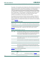
Document information
Info Content
Keywords LPC3220, LPC3230, LPC3240, LPC3250, ARM9, LPC3220/01,
LPC3230/01, LPC3240/01, LPC3250/01, 16/32-bit ARM microcontroller.
Abstract User manual for LPC32x0.

UM10326 All information provided in this document is subject to legal disclaimers. © NXP B.V. 2011. All rights reserved.
User manual Rev. 3 — 22 July 2011 2 of 721
Contact information
For more information, please visit: http://www.nxp.com
For sales office addresses, please send an email to: [email protected]
NXP Semiconductors
UM10326
LPC32x0 User manual
Revision history
Rev Date Description
3 20110722 LPC32x0 user manual
Modifications: System control chapter added.
2 20110504 LPC32x0 user manual
Modifications:
• Voltage domains updated in Table 671, Table 696, and Table 697.
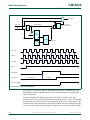
• LCDENAB signal updated in LCD timing diagrams Figure 35 and Figure 36.
• Definition of Bus Keeper (BK) pins updated in Table 670.
• GPI_6 updated to input with bus keeper function.
• Power supply domain for pins SYSX_IN and SYSX_OUT updated in Table 671.
• Description of DBGEN pin function updated in Section 4.6.1 and Table 671.
• Explanation of simultaneous update mode for PWM Motor control Match and Limit
register added in Section 30.7.7.1 “Match and Limit shadow write and operating
registers”.
• Registers SERIAL_ID0 to 3 added for unique serial ID number (Section 3.1.3).
• Updated TAP ID and ETB ID (Table 710).
• Editorial updates.
• Pin functions for touch screen control controller updated: pin T14 has functions
ADIN1/TS_XM and pin U15 has functions ADIN0/TS_YM (see Table 668, Table 669,
Table 255, Table 229, Figure 37.
• Pin selection for touch screen control controller in manual mode updated (TS_YPC
values in Table 231).
• Parts LPC3220/01, LPC3230/01, LPC3240/01, LPC3250/01 added.
1 20090218 Initial LPC32x0 user manual release.

UM10326 All information provided in this document is subject to legal disclaimers. © NXP B.V. 2011. All rights reserved.
User manual Rev. 3 — 22 July 2011 3 of 721
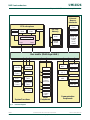
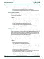
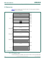
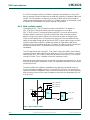
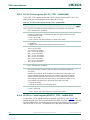
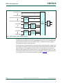
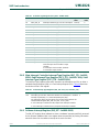
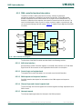
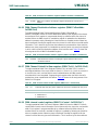
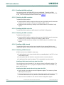
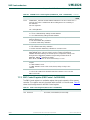
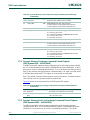
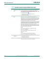
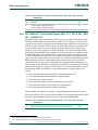
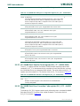
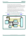
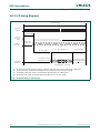
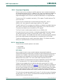
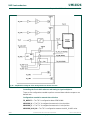
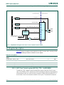
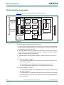
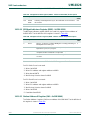
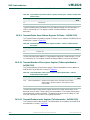
1.1 Introduction
NXP Semiconductor designed the LPC32x0 for embedded applications requiring high
performance and low power consumption.
NXP achieved their performance objectives using an ARM926EJ-S CPU core with a
Vector Floating Point co-processor and a large set of standard peripherals, including USB
On-The-Go. Figure 1 shows a block diagram of the LPC32x0. The LPC32x0 operates at
CPU frequencies up to 266 MHz. The basic ARM926EJ-S CPU Core implementation uses
a Harvard architecture with a 5-stage pipeline. The ARM926EJ-S core also has an
integral Memory Management Unit (MMU) to provide the virtual memory capabilities
required to support the multi-programming demands of modern operating systems. The
basic ARM926EJ-S core also includes a set of DSP instruction extensions including single
cycle MAC operations and native Jazelle Java Byte-code execution in hardware. The NXP
implementation has one 32 kB Instruction Cache and one 32 kB Data Cache.
For low power consumption, the LPC32x0 takes advantage of NXP Semiconductor's
advanced technology development expertise to optimize Intrinsic Power, and software
controlled architectural enhancements to optimize Power Management.
The LPC32x0 also includes 128 to 256 kB of on-chip static RAM, a NAND Flash interface,
an Ethernet MAC, an LCD controller that supports STN and TFT panels, and an external
bus interface that supports SDR and DDR SDRAM as well as static devices. In addition,
the LPC32x0 includes a USB 2.0 Full Speed interface, seven UARTs, two I2C interfaces,
two SPI/SSP ports, two I2S interfaces, two single output PWMs, a motor control PWM,
four general purpose timers with capture inputs and compare outputs, a Secure Digital
(SD) interface, and a 10-bit A/D converter with a touch screen sense option.
UM10326
Chapter 1: LPC32x0 Introductory information
Rev. 3 — 22 July 2011 User manual

UM10326 All information provided in this document is subject to legal disclaimers. © NXP B.V. 2011. All rights reserved.
User manual Rev. 3 — 22 July 2011 4 of 721
NXP Semiconductors
UM10326
Chapter 1: LPC32x0 Introductory information
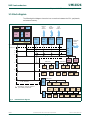
Fig 1. LPC32x0 diagram
External
Memory
Interfaces
System Functions
CPU subsystem
ARM926EJ
Instr Data
I-Cache
32kB
D-Cache
32kB
ETB VFP9
DMA
Controller
ETM9
On-Chip
Memory
ROM
256 kB
SRAM
Other
Peripherals
Bus matrix (Multi-layer AHB)
Watchdog
High Speed
Timer
Millisecond
Timer
Power
Control
PLLs
System
Control
Interrupt
Controller
PWM 1, 2
Touch
Screen/
10-bit A/D
Keyscan
GPIO
Motor
Control
PWM
Communication
Peripherals
USB OTG
UART6
IrDA
UART
1-5, 7
I2C 1, 2
I2S 0, 1
SPI 1, 2
SSP 0, 1
NAND
Flash
SRAM and
SDRAM
(SDR/
DDR)
control
SD Card
Timer
LCD
Ethernet
MAC
RTC
0,1,2,3,4,5

UM10326 All information provided in this document is subject to legal disclaimers. © NXP B.V. 2011. All rights reserved.
User manual Rev. 3 — 22 July 2011 5 of 721
NXP Semiconductors
UM10326
Chapter 1: LPC32x0 Introductory information
1.2 Features
• ARM926EJS processor, running at CPU clock speeds up to 266 MHz
• A Vector Floating Point coprocessor.
• A 32 kB instruction cache and a 32 kB data cache.
• Up to 256 kB of internal SRAM.
• Selectable boot-up from various external devices: NAND Flash, SPI memory, USB,
UART, or static memory.
• A Multi-layer AHB system that provides a separate bus for each AHB master,
including both an instruction and data bus for the CPU, two data busses for the DMA
controller, and another bus for the USB controller, one for the LCD and a final one for
the Ethernet MAC. There are no arbitration delays in the system unless two masters
attempt to access the same slave at the same time.
• An External memory controller for DDR and SDR SDRAM, as well as static devices.
– The address bus provides up to 16 MB for each of the 4 static chip selects.
– The controller provides two dynamic memory chip selects addressing up to
512 MB each.
• Two NAND Flash controllers. One for single level NAND Flash devices and the other
for multi-level NAND Flash devices.
• An Interrupt Controller, supporting 73 interrupt sources.
• An eight channel General Purpose AHB DMA controller (GPDMA) that can be used
with the SD card port, the 14-clock UARTs, I2S ports, and SPI interfaces, as well as
memory-to-memory transfers.
• Serial Interfaces:
– A 10/100 Ethernet MAC with dedicated DMA Controller.
– A USB interface supporting either Device, Host (OHCI compliant), or On-The-Go
(OTG) with an integral DMA controller and dedicated PLL to generate the required
48 MHz USB clock.
– Four standard UARTs with fractional baud rate generation and 64 byte FIFOs. One
of the standard UART’s supports IrDA.
– Three additional 14-clock UARTs intended for on-board communications that
support baudrates up to 921,600 bps when using a 13 MHz main oscillator.All
14-clock UARTs provide 64-byte FIFOs.
– Two SPI controllers.
– Two SSP controllers.
– Two I2C-bus Interfaces with standard open drain pins. The I2C-bus Interfaces
support single master, slave and multi-master I2C configurations.
– Two I2S interfaces, each with separate input and output channels. Each channel
can be operated independently on 3 pins, or both input and output with one I2S
interface can be done on only 4 pins.
• Additional Peripherals:
– LCD controller supporting both STN and TFT panels, with dedicated DMA
controller. Programmable display resolution up to 1024x768.
– Secure Digital (SD) memory card interface.

UM10326 All information provided in this document is subject to legal disclaimers. © NXP B.V. 2011. All rights reserved.
User manual Rev. 3 — 22 July 2011 6 of 721
NXP Semiconductors
UM10326
Chapter 1: LPC32x0 Introductory information
– General purpose input, output, and I/O pins. Includes 12 general purpose input
pins, 24 general purpose output pins, and 51 general purpose I/O pins.
– A touch screen controller, which can alternatively operate as a 10 bit, 400kHz A/D
Converter with input multiplexing from 3 pins.
– Real Time Clock (RTC) with separate power pin. This RTC has a dedicated 32 kHz
oscillator. NXP implemented the RTC in an independent on-chip power domain so
it can remain active while the rest of the chip is not powered. The RTC also
Includes a 32 byte scratch pad memory.
– A 32-bit general purpose high speed timer with a 16-bit pre-scaler. This timer
includes one external capture input pin and a capture connection to the RTC clock.
Interrupts may be generated using 3 match registers.
– Six enhanced Timer/Counters which are identical except for the peripheral base
address. A minimum of two capture inputs and two match outputs are pinned out
for four timers. Timer 1 brings out a third match output, while Timers 2 and 3 bring
out all four match outputs, Timer 4 has one capture register and Timer 5 has no pin
connections.
– A 32-bit Millisecond timer driven from the RTC clock. This timer can generate
interrupts using 2 match registers.
– A Watchdog Timer. The watchdog timer is clocked by PERIPH_CLK.
– Two single output PWM blocks.
– One PWM designed for Motor Control.
– Keyboard scanner function allows automatic scanning of up to an 8x8 key matrix.
– Up to 18 external interrupts.
• Standard ARM Test/Debug interface for compatibility with existing tools.
• Emulation Trace Buffer with 2K x 24 bit RAM allows trace via JTAG.
• Stop mode saves power, while allowing many peripheral functions to restart CPU
activity.
• On-chip crystal oscillator.
• An on-chip PLL allows CPU operation up to the maximum CPU rate without the
requirement for a high frequency crystal. Another PLL allows operation from the 32
kHz RTC clock rather than the external crystal.
• Boundary Scan for simplified board testing.
• User-accessible unique serial ID number for each chip.
• 296 pin TFBGA package.
1.3 Applications
• Consumer
• Medical
• Network Control
• Industrial
• Communications

UM10326 All information provided in this document is subject to legal disclaimers. © NXP B.V. 2011. All rights reserved.
User manual Rev. 3 — 22 July 2011 7 of 721
NXP Semiconductors
UM10326
Chapter 1: LPC32x0 Introductory information
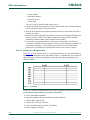
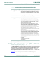
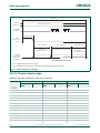
1.4 Ordering Information
[1] Available in Revision “-” and “A”. F = 40 C to +85 C temperature range. Note that Revision “A” parts with and without the /01 suffix are
identical. For example, LPC3220FET296 Revision “A” is identical to LPC3220FET296/01 Revision “A”.
[2] Available starting with Revision “A”.
1.4.1 Ordering options
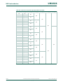
Table 1. Ordering information
Type number Package
Name Description Version
LPC3220FET296
[1]
TFBGA296 plastic thin fine-pitch ball grid array package; 296 balls; body
15x15x0.7 mm
SOT1048-1
LPC3230FET296
[1]
TFBGA296 plastic thin fine-pitch ball grid array package; 296 balls; body
15x15x0.7 mm
SOT1048-1
LPC3240FET296
[1]
TFBGA296 plastic thin fine-pitch ball grid array package; 296 balls; body
15x15x0.7 mm
SOT1048-1
LPC3250FET296
[1]
TFBGA296 plastic thin fine-pitch ball grid array package; 296 balls; body
15x15x0.7 mm
SOT1048-1
LPC3220FET296/01
[2]
TFBGA296 plastic thin fine-pitch ball grid array package; 296 balls; body
15x15x0.7 mm
SOT1048-1
LPC3230FET296/01
[2]
TFBGA296 plastic thin fine-pitch ball grid array package; 296 balls; body
15x15x0.7 mm
SOT1048-1
LPC3240FET296/01
[2]
TFBGA296 plastic thin fine-pitch ball grid array package; 296 balls; body
15x15x0.7 mm
SOT1048-1
LPC3250FET296/01
[2]
TFBGA296 plastic thin fine-pitch ball grid array package; 296 balls; body
15x15x0.7 mm
SOT1048-1
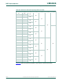
Table 2. Part options
Type number SRAM (kB) 10/100 Ethernet LCD
Controller
Temperature range (°C) Package
LPC3220FET296 128 0 0 -40 to +85 TFBGA296
LPC3230FET296 256 0 1 -40 to +85 TFBGA296
LPC3240FET296 256 1 0 -40 to +85 TFBGA296
LPC3250FET296 256 1 1 -40 to +85 TFBGA296
LPC3220FET296/01 128 0 0 -40 to +85 TFBGA296
LPC3230FET296/01 256 0 1 -40 to +85 TFBGA296
LPC3240FET296/01 256 1 0 -40 to +85 TFBGA296
LPC3250FET296/01 256 1 1 -40 to +85 TFBGA296

UM10326 All information provided in this document is subject to legal disclaimers. © NXP B.V. 2011. All rights reserved.
User manual Rev. 3 — 22 July 2011 8 of 721
NXP Semiconductors
UM10326
Chapter 1: LPC32x0 Introductory information
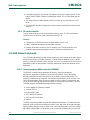
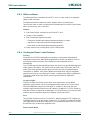
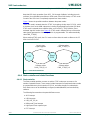
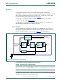
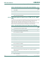
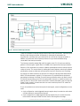
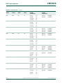
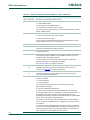
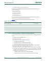
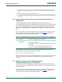
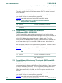
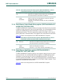
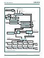
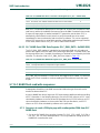
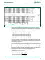
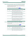
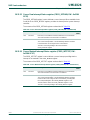
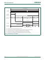
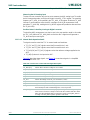
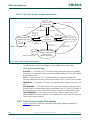
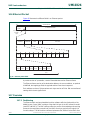
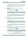
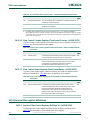
1.5 Block diagram
The following block diagram shows the bus connections between the CPU, peripherals,
and external memory.
Fig 2. LPC32x0 block diagram
ARM
9EJS
MMU
D-Cache
32KB
D-Side
Controller
I-Cache
32KB
I-Side
Controller
Data
Instruction
DMA
controller
Ethernet
10/100
MAC
USB OTG
controller
LCD
controller
Ethernet
PHY
interface
USB
tranceiver
interface
LCD
panel
interface
External
Memory
controller
ROM
16 KB
SRAM
256 KB
MLC
NAND
SLC
NAND
SD
Card
SPI
x 2
I2S
x 2
SSP
x 2
USB
regs
DMA
regs
ETB
regs
SDRAM
regs
Standard UART
x4
I2C
x2
Timers
x6
Watchdog
timer
AHB
to
APB
bridge
Debug
System
Control
14C UART
x3
Key
Scanner
10-bit
ADC/TS
UART
Control
RTC
PWM
x2
Interrupt
Control
GPIO
M1M0
AHB
to
APB
bridge
AHB
to
APB
bridge
Master Layer 0 1 2 3 4 5 6
Slave Port 0
1
7
6
5
3
2
= Master/Slave connection supported
by the multilayer AHB matrix
32 bit, AHB Matrix
APB Slaves
FAB Slaves
AHB Slaves
AHB Slaves
APB Slaves
Port 3
Port 4
Port 0
32-bit wide
external
memory
ETB
ETM 9
VFP9
LCD
regs
Ethernet
regs
Motor Control
PWM

UM10326 All information provided in this document is subject to legal disclaimers. © NXP B.V. 2011. All rights reserved.
User manual Rev. 3 — 22 July 2011 9 of 721
NXP Semiconductors
UM10326
Chapter 1: LPC32x0 Introductory information
1.6 CPU Subsystem
1.6.1 CPU
NXP implemented the LPC32x0 using an ARM926EJ-S CPU core that has a Harvard
architecture and a 5-stage pipeline. To the ARM926EJ-S CPU core, NXP added a 32 kB
Instruction Cache, a 32 kB Data Cache and a Vector Floating Point coprocessor.
The ARM926EJ-S core also has an integral Memory Management Unit (MMU) to provide
the virtual memory capabilities required to support the multi-programming demands of
modern operating systems. The ARM926EJ-S core V5TE instruction set includes DSP
instruction extensions, and can execute native Jazelle Java Byte-code in hardware. The
LPC32x0 operates at CPU frequencies up to 266 MHz.
1.6.2 Vector Floating Point (VFP) coprocessor
The LPC32x0 has a VFP co-processor providing full support for single-precision and
double-precision add, subtract, multiply, divide, and multiply-accumulate operations at
CPU clock speeds. It is compliant with the IEEE 754 standard for binary Floating-Point
Arithmetic. This hardware floating point capability makes the micro controller suitable for
advanced Motor control and DSP applications. The VFP has 3 separate pipelines for
Floating-point MAC operations, divide or square root operations, and Load/Store
operations. These pipelines operate in parallel and can complete execution out of order.
All single-precision instructions execute in one cycle, except the divide and square root
instructions. All double-precision multiply and multiply-accumulate instructions take two
cycles. The VFP also provides format conversions between floating-point and integer
word formats.
1.6.3 Emulation and debugging
The LPC32x0 supports emulation and debugging via a dedicated JTAG serial port. An
Embedded Trace Buffer allows tracing program execution. The dedicated JTAG port
allows debugging of all chip features without impact to any pins that may be used in the
application.
EmbeddedICE
Standard ARM EmbeddedICE logic provides on-chip debug support. The debugging of
the target system requires a host computer running the debugger software and an
EmbeddedICE protocol converter. The EmbeddedICE protocol converter converts the
Remote Debug Protocol commands to the JTAG data needed to access the ARM core.
The ARM core has a Debug Communication Channel function built-in. The debug
communication channel allows a program running on the target to communicate with the
host debugger or another separate host without stopping the program flow or entering the
debug state.
Embedded Trace Buffer
The Embedded Trace Module (ETM) is connected directly to the ARM core. It compresses
the trace information and exports it through a narrow trace port. An internal Embedded
Trace Buffer of 2 k 24 bits captures the trace information under software debugger
control. Data from the Embedded Trace Buffer is recovered by the debug software
through the JTAG port.

UM10326 All information provided in this document is subject to legal disclaimers. © NXP B.V. 2011. All rights reserved.
User manual Rev. 3 — 22 July 2011 10 of 721
NXP Semiconductors
UM10326
Chapter 1: LPC32x0 Introductory information
The trace contains information about when the ARM core switches between states.
Instruction trace (or PC trace) shows the flow of execution of the processor and provides a
list of all the instructions that were executed. Instruction trace is significantly compressed
by only broadcasting branch addresses as well as a set of status signals that indicate the
pipeline status on a cycle by cycle basis. For data accesses either data or address or both
can be traced.
1.7 AHB Bus Architecture
The LPC32x0 has a multi-layer AHB matrix for inter-block communication. AHB is an
ARM defined high-speed bus, which is part of the ARM bus architecture. AHB is a
high-bandwidth low-latency bus that supports multi-master arbitration and a bus
grant/request mechanism. For systems that have only one (CPU), or two (CPU and DMA)
bus masters a simple AHB works well. However, if a system requires multiple bus masters
and the CPU needs access to external memory, a single AHB bus can cause a bottleneck.
In addition to the AHB matrix the LPC32x0 has two peripheral busses the APB and the
FAB. A short description of the busses are described in the following sections.
1.7.1 AHB Matrix
To increase performance, the LPC32x0 uses an expanded AHB architecture known as
Multi-layer AHB. A Multi-layer AHB replaces the request/grant and arbitration mechanism
used in a simple AHB with an interconnect matrix that moves arbitration out toward the
slave devices. Thus, if a CPU and a DMA controller want access to the same memory, the
interconnect matrix arbitrates between the two when granting access to the memory. This
advanced architecture allows simultaneous access by bus masters to different resources
with an increase in arbitration complexity. In this architectural implementation, removing
guaranteed central arbitration and allowing more than one bus master to be active at the
same time provides better overall micro controller performance.
In the LPC32x0, the Multi-Layer AHB system has a separate bus for each of seven AHB
Masters:
• CPU Data bus
• CPU Instruction bus
• General purpose DMA Master 0
• General purpose DMA Master 1
• Ethernet Controller
• USB Controller
• LCD Controller
There are no arbitration delays unless two masters attempt to access the same slave at
the same time.
1.7.2 APB bus
Many peripheral functions are accessed by on-chip APB busses that are attached to the
higher speed AHB bus. The APB bus performs reads and writes to peripheral registers in
three peripheral clocks.

UM10326 All information provided in this document is subject to legal disclaimers. © NXP B.V. 2011. All rights reserved.
User manual Rev. 3 — 22 July 2011 11 of 721
NXP Semiconductors
UM10326
Chapter 1: LPC32x0 Introductory information
1.7.3 FAB bus
Some peripherals are placed on a special bus called FAB that allows faster CPU access
to those peripheral functions. A write access to FAB peripherals takes a single AHB clock
and a read access to FAB peripherals takes two AHB clocks.
1.8 Internal Memory
On-Chip SRAM (IRAM)
On-chip SRAM may be used for code and/or data storage. The SRAM may be accessed
as 8, 16, or 32 bit memory. The LPC32x0 provides 256 kB of internal SRAM.
On-Chip ROM
An on-chip 16 kB ROM contains the necessary code to load code from one of four
sources, UART5, SSP0 (in SPI mode), EMC (CS0 SRAM) memory, or NAND FLASH, and
copy it to IRAM. The code loaded to IRAM will typically be FLASH programming software.
The boot process is handled by an on-chip bootloader that looks at the state of a pin
(GPI_1) to see if it should attempt to download a program over a serial link (UART5) or
one of three alternate sources, SSP0, EMC (CS0) memory, and NAND Flash and then
branch to its entry point and execute. If the GPI_1 pin is low it will boot from UART5
(SERVICE_N boot), if it is set high, it will test in sequence each of the remaining possible
sources for the presence of download code. The bootloader will first test for boot code in
the SSP0, if this fails it will test for boot code in EMC memory and if this fails it will test the
NAND Flash for boot code.
The bootloader reserves a small portion (8kB from 0x0000 E000 to 0x0000 FFFF) on the
Internal SRAM during the boot process. This space is no longer used once the boot loader
has passed control to the downloaded code.
1.9 External Memory Interfaces
The LPC32x0 includes three external memory interfaces.
• an interface supporting two NAND Flash controllers, an Multi-level and a Single-level.
• an external memory controller (EMC) interface for SDRAM, DDR SDRAM, and Static
Memory devices.
• a Secure Digital Memory Controller (SDCARD) interface.
1.9.1 NAND flash controller Interface
The LPC32x0 includes two NAND flash controllers, one for multi-level NAND flash
devices and one for single-level NAND flash devices. The two NAND flash controllers use
the same pins to interface to external NAND flash devices, so only one interface is active
at a time.
Multi-Level Cell (MLC) NAND flash controller
The MLC NAND flash controller interfaces to either multi-level or single-level NAND flash
devices. An external NAND flash device is used to allow the bootloader to automatically
load a portion of the application code into internal SRAM for execution following reset.

UM10326 All information provided in this document is subject to legal disclaimers. © NXP B.V. 2011. All rights reserved.
User manual Rev. 3 — 22 July 2011 12 of 721
NXP Semiconductors
UM10326
Chapter 1: LPC32x0 Introductory information
The MLC NAND flash controller supports up to 2 Gbit devices with small (528 byte) or
large (2114 byte) pages. Programmable NAND timing parameters allow support for a
variety of NAND flash devices. A built-in Reed-Solomon encoder/decoder provides error
detection and correction capability. A 528 byte data buffer reduces the need for CPU
supervision during loading. The MLC NAND flash controller also provides DMA support.
Single-Level Cell (SLC) NAND flash controller
The SLC NAND flash controller interfaces to single-level NAND flash devices up to 2 Gbit
in size. DMA page transfers are supported, including a 20 byte DMA read and write FIFO.
Hardware support for ECC (Error Checking and Correction) is included for the main data
area. Software can correct a single bit error.
1.9.2 External Memory Controller Interface
The LPC32x0 includes an External Memory Controller (EMC) that supports SDRAM, DDR
SDRAM, and Static memory devices. The EMC provides an interface between the system
bus and external (off-chip) memory devices.
The controller supports SDR SDRAM devices of 64/128/256/512 Mbit in size, as well as
16-bit wide data bus DDR SDRAM devices of 64/128/256/512 Mbit in size. Two dynamic
memory chip selects are supplied, supporting two groups of SDRAM
• EMC_DYCS0_N in the address range 0x8000 0000 to 0x9FFF FFFF
• EMC_DYCS1_N in the address range 0xA000 0000 to 0xBFFF FFFF
The memory controller also supports 8-bit, 16-bit, and 32-bit wide asynchronous static
memory devices, including RAM, ROM, and Flash, with or without asynchronous page
mode. Four static memory chip selects are supplied for SRAM devices.
• EMC_CS0_N in the address range 0xE000 0000 to 0xE0FF FFFF
• EMC_CS1_N in the address range 0xE100 0000 to 0xE1FF FFFF
• EMC_CS2_N in the address range 0xE200 0000 to 0xE2FF FFFF
• EMC_CS3_N in the address range 0xE300 0000 to 0xE3FF FFFF
The SDRAM controller uses three data ports to allow simultaneous requests from multiple
on-chip AHB bus masters and has the following features.
• Dynamic memory interface supports SDRAM, DDR-SDRAM, and low-power variants.
It also supports Micron SyncFlash types of memory
• Read and write buffers to reduce latency and improve performance
• Static memory features include
– asynchronous page mode read
– programmable wait states
– bus turnaround cycles
– output enable and write enable delays
– extended wait
• Power-saving modes dynamically control EMC_CKE and EMC_CLK
• Dynamic memory self-refresh mode supported by software

UM10326 All information provided in this document is subject to legal disclaimers. © NXP B.V. 2011. All rights reserved.
User manual Rev. 3 — 22 July 2011 13 of 721
NXP Semiconductors
UM10326
Chapter 1: LPC32x0 Introductory information
• Controller supports 2K, 4K, and 8K row address synchronous memory parts. That is,
typical 512Mb, 256Mb, 128Mb, and 16Mb parts, with 8, 16, or 32 DQ (data) bits per
device
• Two reset domains enable dynamic memory contents to be preserved over a soft
reset
• This controller does NOT Support Synchronous static memory devices (burst mode
devices)
1.9.3 SD card controller
The SD interface allows access to external SD memory cards. The SD card interface
conforms to the SD Memory Card Specification Version 1.01.
Features
• Conformance to the SD Memory Card Specification Version 1.01.
• DMA is supported through the system DMA controller.
• Provides all functions specific to the SD memory card. These include the clock
generation unit, power management control, command and data transfer.
1.10 AHB Master Peripherals
The LPC32x0 implements four AHB master peripherals, which include a General Purpose
Direct Memory Access (GPDMA) controller, a 10/100 Ethernet Media Access Controller
(MAC), a Universal Serial Bus (USB) controller, and an LCD Controller. Each of these four
peripherals contain an integral DMA controller optimized to support the demands of the
peripheral.
1.10.1 General purpose DMA controller (GPDMA)
The GPDMA controller allows peripheral-to memory, memory-to-peripheral,
peripheral-to-peripheral, and memory-to-memory transactions. Each DMA stream
provides unidirectional serial DMA transfers for a single source and destination. For
example, a bidirectional port requires one stream for transmit and one for receives. The
source and destination areas can each be either a memory region or a peripheral, and
can be accessed through the same AHB master or one area by each master. The DMA
controller supports the following peripheral device transfers.
• Secure Digital (SD) Memory interface
• 14-clock UART’s
• I2S0 and I2S1 Ports
• SPI1 and SPI2 Interfaces
• SSP0 and SSP1 interfaces
• Memory
The DMA controls eight DMA channels with hardware prioritization. The DMA controller
interfaces to the system via two AHB bus masters, each with a full 32-bit data bus width.
DMA operations may be set up for 8-bit, 16-bit, and 32-bit data widths, and can be either
big-endian or little-endian. Incrementing or non-incrementing addressing for source and

UM10326 All information provided in this document is subject to legal disclaimers. © NXP B.V. 2011. All rights reserved.
User manual Rev. 3 — 22 July 2011 14 of 721
NXP Semiconductors
UM10326
Chapter 1: LPC32x0 Introductory information
destination are supported, as well as programmable DMA burst size. Scatter or gather
DMA is supported through the use of linked lists. This means that the source and
destination areas do not have to occupy contiguous areas of memory.
1.10.2 Ethernet MAC
The Ethernet block contains a full featured 10 Mbit/s or 100 Mbit/s Ethernet MAC
designed to provide optimized performance through the use of DMA hardware
acceleration. Features include a generous suite of control registers, half or full duplex
operation, flow control, control frames, hardware acceleration for transmit retry, receive
packet filtering and wake-up on LAN activity. Automatic frame transmission and reception
with scatter-gather DMA off-loads many operations from the CPU. The Ethernet block and
the CPU share a dedicated AHB subsystem that is used to access the Ethernet SRAM for
Ethernet data, control, and status information. All other AHB traffic in the LPC32x0 takes
place on a different AHB subsystem, effectively separating Ethernet activity from the rest
of the system. The Ethernet DMA can also access off-chip memory via the EMC, as well
as the SRAM located on another AHB. However, using memory other than the Ethernet
SRAM, especially off-chip memory, will slow Ethernet access to memory and increase the
loading of its AHB. The Ethernet block interfaces between an off-chip Ethernet PHY using
the Media Independent Interface (MII) or Reduced MII (RMII) protocol and the on-chip
Media Independent Interface Management (MIIM) serial bus.
Features
• Ethernet standards support:
– Supports 10 Mbit/s or 100 Mbit/s PHY devices including 10 Base-T, 100 Base-TX,
100 Base-FX, and 100 Base-T4
– Fully compliant with IEEE standard 802.3
– Fully compliant with 802.3x Full Duplex Flow Control and Half Duplex back
pressure
– Flexible transmit and receive frame options
– Virtual Local Area Network (VLAN) frame support
• Memory management
– Independent transmit and receive buffers memory mapped to shared SRAM
– DMA managers with scatter/gather DMA and arrays of frame descriptors
– Memory traffic optimized by buffering and pre-fetching
• Enhanced Ethernet features:
– Receive filtering
– Multicast and broadcast frame support for both transmit and receive
– Optional automatic Frame Check Sequence (FCS) insertion with Circular
Redundancy Check (CRC) for transmit
– Selectable automatic transmit frame padding
– Over-length frame support for both transmit and receive allows any length frames
– Promiscuous receive mode
– Automatic collision back-off and frame retransmission

UM10326 All information provided in this document is subject to legal disclaimers. © NXP B.V. 2011. All rights reserved.
User manual Rev. 3 — 22 July 2011 15 of 721
NXP Semiconductors
UM10326
Chapter 1: LPC32x0 Introductory information
– Includes power management by clock switching. Wake-on-LAN power
management support allows system wake-up: using the receive filters or a magic
frame detection filter
• Physical interface
– Attachment of external PHY chip through standard MII or RMII interface
– PHY register access is available via the MIIM interface
1.10.3 USB interface
The LPC32x0 supports USB in either DEVICE, HOST, or OTG configuration.
1.10.3.1 USB DEVICE controller
The USB device controller enables 12 Mbit/s data exchange with a USB host controller. It
consists of register interface, serial interface engine, endpoint buffer memory and DMA
controller. The serial interface engine decodes the USB data stream and writes data to the
appropriate end point buffer memory. The status of a completed USB transfer or error
condition is indicated via status registers. An interrupt is also generated if enabled. The
DMA controller when enabled transfers data between the endpoint buffer and the USB
RAM.
Features
• Fully compliant with USB 2.0 full-speed specification.
• Supports 32 physical (16 logical) endpoints.
• Supports control, bulk, interrupt and isochronous endpoints.
• Scalable realization of endpoints at run time.
• Endpoint maximum packet size selection (up to USB maximum specification) by
software at run time.
• RAM message buffer size based on endpoint realization and maximum packet size.
• Supports bus-powered capability with low suspend current.
• Supports DMA transfer on all non-control endpoints.
• One duplex DMA channel serves all endpoints.
• Allows dynamic switching between CPU controlled and DMA modes.
• Double buffer implementation for bulk and isochronous endpoints.
1.10.3.2 USB HOST controller
The host controller enables data exchange with various USB devices attached to the bus.
It consists of register interface, serial interface engine and DMA controller. The register
interface complies to the OHCI specification.
Features
• OHCI compliant.
• OHCI specifies the operation and interface of the USB host controller and SW driver.
• The host controller has four USB states visible to the SW driver:
– USBOperational: Process lists and generate SOF tokens.
– USBReset: Forces reset signaling on the bus, SOF disabled.

UM10326 All information provided in this document is subject to legal disclaimers. © NXP B.V. 2011. All rights reserved.
User manual Rev. 3 — 22 July 2011 16 of 721
NXP Semiconductors
UM10326
Chapter 1: LPC32x0 Introductory information
– USBSuspend: Monitor USB for wake-up activity.
– USBResume: Forces resume signaling on the bus.
• HCCA register points to interrupt and isochronous descriptors list.
• ControlHeadED and BulkHeadED registers point to control and bulk descriptors list.
1.10.3.3 USB OTG Controller
USB OTG (On-The-Go) is a supplement to the USB 2.0 specification that augments the
capability of existing mobile devices and USB peripherals by adding host functionality for
connection to USB peripherals.
Features
• Fully compliant with On-The-Go supplement to the USB Specification 2.0 Revision
1.0.
• Supports Host Negotiation Protocol (HNP) and Session Request Protocol (SRP) for
dual-role devices under software control. HNP is partially implemented in hardware.
• Provides programmable timers required for HNP and SRP.
• Supports slave mode operation through AHB slave interface.
• Supports the OTG ATX from NXP (ISP 1301) or any external CEA-2011OTG
specification compliant ATX.
1.10.4 LCD Controller
The LCD controller provides all of the necessary control signals to interface directly to a
variety of color and monochrome LCD panels. Both STN (single and dual panel) and TFT
panels can be operated. The display resolution is selectable and can be up to 1024 × 768
pixels. Several color modes are provided, up to a 24-bit true-color non-palettized mode.
An on-chip 512-byte color palette allows reducing bus utilization (i.e. memory size of the
displayed data) while still supporting a large number of colors.
The LCD interface includes its own DMA controller to allow it to operate independently of
the CPU and other system functions. A built-in FIFO acts as a buffer for display data,
providing flexibility for system timing. Hardware cursor support can further reduce the
amount of CPU time needed to operate the display.
Features
• AHB bus master interface to access frame buffer
• Setup and control via a separate AHB slave interface
• Dual 16-deep programmable 64-bit wide FIFOs for buffering incoming display data
• Supports single and dual-panel monochrome Super Twisted Nematic (STN) displays
with 4-bit or 8-bit interfaces
• Supports single and dual-panel color STN displays
• Supports Thin Film Transistor (TFT) color displays
• Programmable display resolution including, but not limited to: 320 × 200, 320 × 240,
640 × 200, 640 × 240, 640 × 480, 800 × 600, and 1024 × 768
• Hardware cursor support for single-panel displays
• 15 gray-level monochrome, 3375 color STN, and 32 K color palettized TFT support

UM10326 All information provided in this document is subject to legal disclaimers. © NXP B.V. 2011. All rights reserved.
User manual Rev. 3 — 22 July 2011 17 of 721
NXP Semiconductors
UM10326
Chapter 1: LPC32x0 Introductory information
• 1, 2, or 4 bits-per-pixel (bpp) palettized displays for monochrome STN
• 1, 2, 4, or 8 bpp palettized color displays for color STN and TFT
• 16 bpp true-color non-palettized, for color STN and TFT
• 24 bpp true-color non-palettized, for color TFT
• Programmable timing for different display panels
• 256 entry, 16-bit palette RAM, arranged as a 128 × 32-bit RAM
• Frame, line, and pixel clock signals
• AC bias signal for STN, data enable signal for TFT panels
• Supports little and big-endian, and Windows CE data formats
• LCD panel clock may be generated from the peripheral clock, or from a clock input pin
1.11 System Functions
To enhance the performance of the LPC32x0 incorporates the following System
Functions, an Interrupt Controller (INTC), a Watchdog timer, a Millisecond Timer, and
several Power Control Features. These functions are described in the following sections
1.11.1 Interrupt controller
The interrupt controller is comprised of three basic interrupt controller blocks, supporting a
total of 73 interrupt sources. Each interrupt source can be individually enabled/disabled
and configured for high or low level triggering, or rising or falling edge triggering. Each
interrupt may also be steered to either the FIQ or IRQ input of the ARM9. Raw interrupt
status and masked interrupt status registers allow versatile condition evaluation. In
addition to peripheral functions, each of the six general purpose input/output pins and
12 general purpose input pins are connected directly to the interrupt controller.
1.11.2 Watchdog timer
The watchdog timer block is clocked by the main peripheral clock, which clocks a 32-bit
counter. A match register is compared to the Timer. When configured for watchdog
functionality, a match drives the match output low. The match output is gated with an
enable signal that gives the opportunity to generate two type of reset signal: one that only
resets chip internally, and another that goes through a programmable pulse generator
before it goes to the external pin RESOUT_N and to the internal chip reset.
Features
• Programmable 32-bit timer.
• Internally resets the device if not periodically reloaded.
• Flag to indicate that a watchdog reset has occurred.
• Programmable watchdog pulse output on RESOUT_N pin.
• Can be used as a standard timer if watchdog is not used.
• Pause control to stop counting when core is in debug state.

UM10326 All information provided in this document is subject to legal disclaimers. © NXP B.V. 2011. All rights reserved.
User manual Rev. 3 — 22 July 2011 18 of 721
NXP Semiconductors
UM10326
Chapter 1: LPC32x0 Introductory information
1.11.3 Millisecond timer
The millisecond timer is clocked by 32 kHz RTC clock, so a pre-scaler is not needed to
obtain a lower count rate.
The millisecond timer includes three match registers that are compared to the
Timer/Counter value. A match can generate an interrupt and the cause the Timer/Counter
either continue to run, stop, or be reset.
Features
• 32-bit Timer/Counter, running from the 32 kHz RTC clock.
• Counter or Timer operation.
• Three 32-bit match registers that allow:
– Continuous operation with optional interrupt generation on match.
– Stop timer on match with optional interrupt generation.
– Reset timer on match with optional interrupt generation.
• Pause control to stop counting when core is in debug state.
1.11.4 Clocking and Power Control Features
Clocking
Clocking in the LPC32x0 is designed to be versatile, so that system and peripheral
requirements may be met, while allowing optimization of power consumption. Clocks to
most functions may be turned off if not needed and some peripherals do this
automatically.
The LPC32x0 supports three operational modes, two of which are specifically designed to
reduce power consumption. The modes are: RUN mode, Direct RUN mode, and STOP
mode.These three operational modes give control over processing speed and power
consumption. In addition, clock rates to different functional blocks may be changed by
switching clock sources, reconfiguring PLL values, or altering clock divider configurations.
This allows a trade-off of power versus processing speed based on application
requirements.
Crystal Oscillator
The main oscillator is the basis for the clocks most chip functions use by default.
Optionally, many functions can be clocked instead by the output of a PLL (with a fixed
397x rate multiplication) which runs from the RTC oscillator. In this mode, the main
oscillator may be turned off unless the USB interface is enabled. If a SYSCLK frequency
other than 13 MHz is required in the application, or if the USB block is not used, the main
oscillator may be used with a frequency of between 1 MHz and 20 MHz.
PLLs
The LPC32x0 includes three PLLs: The 397x PLL allows boosting the RTC frequency to
13.008896 MHz for use as the primary system clock. The USB PLL provides the 48 MHz
clock required by the USB block; and the HCLK PLL provides the basis for the CPU clock,
the AHB bus clock, and the main peripheral clock.
Power Control Modes

UM10326 All information provided in this document is subject to legal disclaimers. © NXP B.V. 2011. All rights reserved.
User manual Rev. 3 — 22 July 2011 19 of 721
NXP Semiconductors
UM10326
Chapter 1: LPC32x0 Introductory information
The LPC32x0 supports three operational modes, two of which are specifically designed to
reduce power consumption. The modes are: Run mode, Direct Run mode, and Stop
mode.
Run mode is the normal operating mode for applications that require the CPU, AHB bus,
or any peripheral function other than the USB block to run faster than the main oscillator
frequency. In Run mode, the CPU can run at up to 266 MHz and the AHB bus can run at
up to 133 MHz.
Direct Run mode allows reducing the CPU and AHB bus rates in order to save power.
Direct Run mode can also be the normal operating mode for applications that do not
require the CPU, AHB bus, or any peripheral function other than the USB block to run
faster than the main oscillator frequency. Direct Run mode is the default mode following
chip reset.
Stop mode causes all CPU and AHB operation to cease, and stops clocks to peripherals
other than the USB block.
Reset
Reset is accomplished by an active low signal on the RESET_N input pin. A reset pulse
with a minimum width of 10 main oscillator clocks after the oscillator is stable is required to
guarantee a valid chip reset. At power-up, 10 milliseconds should be allowed for the
oscillator to start up and stabilize after V
DD
reaches operational voltage. An internal reset
with a minimum duration of 10 clock pulses will also be applied if the watchdog timer
generates an internal device reset.
The RESET_N pin is located in the RTC power domain. This means that the RTC power
must be present for an external reset to have any effect. The RTC power domain
nominally runs from 1.2 V, but the RESET_N pin can be driven as high as 1.95 V.
The RESET_N pin is also used to isolate the RTC power domains from other on chip
power domains.To minimize power consumption in the RTC power domain while power is
removed from other power domains, the RESET_N pin must be held low.
1.12 Serial communication peripherals
In addition to the Ethernet MAC and USB interfaces there many more serial
Communication peripheral interfaces on the LPC32x0. Here is a list of the available serial
communication interfaces.
• seven UARTs; four Standard UARTs and three 14-clock UARTs
• two SPI Serial I/O Controllers
• two SSP Serial I/O Controllers
• two I2C Serial I/O Controllers
• two I2S Audio Controllers
A short functional description of each of these peripherals is provided in the following
sections.

UM10326 All information provided in this document is subject to legal disclaimers. © NXP B.V. 2011. All rights reserved.
User manual Rev. 3 — 22 July 2011 20 of 721
NXP Semiconductors
UM10326
Chapter 1: LPC32x0 Introductory information
1.12.1 UARTs
The LPC32x0 contains seven UARTs. Four are standard UARTs, and three are 14-clock
UARTs.
Standard UARTs — The four standard UARTs are downwards compatible with the
INS16Cx50. These UARTs support rates up to 460800 bit/s from a 13 MHz peripheral
clock.
Features
• Each standard UART has 64 byte Receive and Transmit FIFOs.
• Receiver FIFO trigger points at 16 B, 32 B, 48 B, and 60 B.
• Transmitter FIFO trigger points at 0 B, 4 B, 8 B, and 16 B.
• Register locations conform to 16C550 industry standard.
• Each standard UART has a fractional rate pre-divider and an internal baud rate
generator.
• The standard UARTs support three clocking modes: on, off, and auto-clock. The
auto-clock mode shuts off the clock to the UART when it is idle.
• UART 6 includes an IrDA mode to support infrared communication.
• The standard UARTs are designed to support data rates of (2400, 4800, 9600,
19200, 38400, 57600, 115200, 230400, 460800) bit/s.
• Each UART includes an internal loopback mode.
14-clock UARTs — The three 14-clock UARTs are designed to support rates up to
921600 bit/s from a 13 MHz peripheral clock, for on-board communication in low noise
conditions. This is accomplished by changing the oversampling from 16 to 14, and
altering the rate generation logic.
Features
• Each 14-clock UART has 64 byte Receive and Transmit FIFOs.
• Receiver FIFO trigger points at 1 B, 4 B, 8 B, 16 B, 32 B, and 48 B.
• Transmitter FIFO trigger points at 0 B, 4 B, and 8 B.
• Each 14-clock UART has an internal baud rate generator.
• The 14-clock UARTs are designed to support data rates of (2400, 4800, 9600, 19200,
38400, 57600, 115200, 230400, 460800, 921600) bit/s.
• Each UART includes an internal loopback mode.
1.12.2 SPI serial I/O controller
The LPC32x0 has two Serial Peripheral Interfaces (SPI). The SPI is a 3-wire serial
interface that is able to interface with a large range of serial peripheral or memory devices
(SPI mode 0 to 3 compatible slave devices).
Only a single master and a single slave can communicate on the interface during a given
data transfer. During a data transfer the master always sends a byte of data to the slave,
and the slave always sends a byte of data to the master. The SPI implementation on the
LPC32x0 does not support operation as a slave.
Page is loading ...
Page is loading ...
Page is loading ...
Page is loading ...
Page is loading ...
Page is loading ...
Page is loading ...
Page is loading ...
Page is loading ...
Page is loading ...
Page is loading ...
Page is loading ...
Page is loading ...
Page is loading ...
Page is loading ...
Page is loading ...
Page is loading ...
Page is loading ...
Page is loading ...
Page is loading ...
Page is loading ...
Page is loading ...
Page is loading ...
Page is loading ...
Page is loading ...
Page is loading ...
Page is loading ...
Page is loading ...
Page is loading ...
Page is loading ...
Page is loading ...
Page is loading ...
Page is loading ...
Page is loading ...
Page is loading ...
Page is loading ...
Page is loading ...
Page is loading ...
Page is loading ...
Page is loading ...
Page is loading ...
Page is loading ...
Page is loading ...
Page is loading ...
Page is loading ...
Page is loading ...
Page is loading ...
Page is loading ...
Page is loading ...
Page is loading ...
Page is loading ...
Page is loading ...
Page is loading ...
Page is loading ...
Page is loading ...
Page is loading ...
Page is loading ...
Page is loading ...
Page is loading ...
Page is loading ...
Page is loading ...
Page is loading ...
Page is loading ...
Page is loading ...
Page is loading ...
Page is loading ...
Page is loading ...
Page is loading ...
Page is loading ...
Page is loading ...
Page is loading ...
Page is loading ...
Page is loading ...
Page is loading ...
Page is loading ...
Page is loading ...
Page is loading ...
Page is loading ...
Page is loading ...
Page is loading ...
Page is loading ...
Page is loading ...
Page is loading ...
Page is loading ...
Page is loading ...
Page is loading ...
Page is loading ...
Page is loading ...
Page is loading ...
Page is loading ...
Page is loading ...
Page is loading ...
Page is loading ...
Page is loading ...
Page is loading ...
Page is loading ...
Page is loading ...
Page is loading ...
Page is loading ...
Page is loading ...
Page is loading ...
Page is loading ...
Page is loading ...
Page is loading ...
Page is loading ...
Page is loading ...
Page is loading ...
Page is loading ...
Page is loading ...
Page is loading ...
Page is loading ...
Page is loading ...
Page is loading ...
Page is loading ...
Page is loading ...
Page is loading ...
Page is loading ...
Page is loading ...
Page is loading ...
Page is loading ...
Page is loading ...
Page is loading ...
Page is loading ...
Page is loading ...
Page is loading ...
Page is loading ...
Page is loading ...
Page is loading ...
Page is loading ...
Page is loading ...
Page is loading ...
Page is loading ...
Page is loading ...
Page is loading ...
Page is loading ...
Page is loading ...
Page is loading ...
Page is loading ...
Page is loading ...
Page is loading ...
Page is loading ...
Page is loading ...
Page is loading ...
Page is loading ...
Page is loading ...
Page is loading ...
Page is loading ...
Page is loading ...
Page is loading ...
Page is loading ...
Page is loading ...
Page is loading ...
Page is loading ...
Page is loading ...
Page is loading ...
Page is loading ...
Page is loading ...
Page is loading ...
Page is loading ...
Page is loading ...
Page is loading ...
Page is loading ...
Page is loading ...
Page is loading ...
Page is loading ...
Page is loading ...
Page is loading ...
Page is loading ...
Page is loading ...
Page is loading ...
Page is loading ...
Page is loading ...
Page is loading ...
Page is loading ...
Page is loading ...
Page is loading ...
Page is loading ...
Page is loading ...
Page is loading ...
Page is loading ...
Page is loading ...
Page is loading ...
Page is loading ...
Page is loading ...
Page is loading ...
Page is loading ...
Page is loading ...
Page is loading ...
Page is loading ...
Page is loading ...
Page is loading ...
Page is loading ...
Page is loading ...
Page is loading ...
Page is loading ...
Page is loading ...
Page is loading ...
Page is loading ...
Page is loading ...
Page is loading ...
Page is loading ...
Page is loading ...
Page is loading ...
Page is loading ...
Page is loading ...
Page is loading ...
Page is loading ...
Page is loading ...
Page is loading ...
Page is loading ...
Page is loading ...
Page is loading ...
Page is loading ...
Page is loading ...
Page is loading ...
Page is loading ...
Page is loading ...
Page is loading ...
Page is loading ...
Page is loading ...
Page is loading ...
Page is loading ...
Page is loading ...
Page is loading ...
Page is loading ...
Page is loading ...
Page is loading ...
Page is loading ...
Page is loading ...
Page is loading ...
Page is loading ...
Page is loading ...
Page is loading ...
Page is loading ...
Page is loading ...
Page is loading ...
Page is loading ...
Page is loading ...
Page is loading ...
Page is loading ...
Page is loading ...
Page is loading ...
Page is loading ...
Page is loading ...
Page is loading ...
Page is loading ...
Page is loading ...
Page is loading ...
Page is loading ...
Page is loading ...
Page is loading ...
Page is loading ...
Page is loading ...
Page is loading ...
Page is loading ...
Page is loading ...
Page is loading ...
Page is loading ...
Page is loading ...
Page is loading ...
Page is loading ...
Page is loading ...
Page is loading ...
Page is loading ...
Page is loading ...
Page is loading ...
Page is loading ...
Page is loading ...
Page is loading ...
Page is loading ...
Page is loading ...
Page is loading ...
Page is loading ...
Page is loading ...
Page is loading ...
Page is loading ...
Page is loading ...
Page is loading ...
Page is loading ...
Page is loading ...
Page is loading ...
Page is loading ...
Page is loading ...
Page is loading ...
Page is loading ...
Page is loading ...
Page is loading ...
Page is loading ...
Page is loading ...
Page is loading ...
Page is loading ...
Page is loading ...
Page is loading ...
Page is loading ...
Page is loading ...
Page is loading ...
Page is loading ...
Page is loading ...
Page is loading ...
Page is loading ...
Page is loading ...
Page is loading ...
Page is loading ...
Page is loading ...
Page is loading ...
Page is loading ...
Page is loading ...
Page is loading ...
Page is loading ...
Page is loading ...
Page is loading ...
Page is loading ...
Page is loading ...
Page is loading ...
Page is loading ...
Page is loading ...
Page is loading ...
Page is loading ...
Page is loading ...
Page is loading ...
Page is loading ...
Page is loading ...
Page is loading ...
Page is loading ...
Page is loading ...
Page is loading ...
Page is loading ...
Page is loading ...
Page is loading ...
Page is loading ...
Page is loading ...
Page is loading ...
Page is loading ...
Page is loading ...
Page is loading ...
Page is loading ...
Page is loading ...
Page is loading ...
Page is loading ...
Page is loading ...
Page is loading ...
Page is loading ...
Page is loading ...
Page is loading ...
Page is loading ...
Page is loading ...
Page is loading ...
Page is loading ...
Page is loading ...
Page is loading ...
Page is loading ...
Page is loading ...
Page is loading ...
Page is loading ...
Page is loading ...
Page is loading ...
Page is loading ...
Page is loading ...
Page is loading ...
Page is loading ...
Page is loading ...
Page is loading ...
Page is loading ...
Page is loading ...
Page is loading ...
Page is loading ...
Page is loading ...
Page is loading ...
Page is loading ...
Page is loading ...
Page is loading ...
Page is loading ...
Page is loading ...
Page is loading ...
Page is loading ...
Page is loading ...
Page is loading ...
Page is loading ...
Page is loading ...
Page is loading ...
Page is loading ...
Page is loading ...
Page is loading ...
Page is loading ...
Page is loading ...
Page is loading ...
Page is loading ...
Page is loading ...
Page is loading ...
Page is loading ...
Page is loading ...
Page is loading ...
Page is loading ...
Page is loading ...
Page is loading ...
Page is loading ...
Page is loading ...
Page is loading ...
Page is loading ...
Page is loading ...
Page is loading ...
Page is loading ...
Page is loading ...
Page is loading ...
Page is loading ...
Page is loading ...
Page is loading ...
Page is loading ...
Page is loading ...
Page is loading ...
Page is loading ...
Page is loading ...
Page is loading ...
Page is loading ...
Page is loading ...
Page is loading ...
Page is loading ...
Page is loading ...
Page is loading ...
Page is loading ...
Page is loading ...
Page is loading ...
Page is loading ...
Page is loading ...
Page is loading ...
Page is loading ...
Page is loading ...
Page is loading ...
Page is loading ...
Page is loading ...
Page is loading ...
Page is loading ...
Page is loading ...
Page is loading ...
Page is loading ...
Page is loading ...
Page is loading ...
Page is loading ...
Page is loading ...
Page is loading ...
Page is loading ...
Page is loading ...
Page is loading ...
Page is loading ...
Page is loading ...
Page is loading ...
Page is loading ...
Page is loading ...
Page is loading ...
Page is loading ...
Page is loading ...
Page is loading ...
Page is loading ...
Page is loading ...
Page is loading ...
Page is loading ...
Page is loading ...
Page is loading ...
Page is loading ...
Page is loading ...
Page is loading ...
Page is loading ...
Page is loading ...
Page is loading ...
Page is loading ...
Page is loading ...
Page is loading ...
Page is loading ...
Page is loading ...
Page is loading ...
Page is loading ...
Page is loading ...
Page is loading ...
Page is loading ...
Page is loading ...
Page is loading ...
Page is loading ...
Page is loading ...
Page is loading ...
Page is loading ...
Page is loading ...
Page is loading ...
Page is loading ...
Page is loading ...
Page is loading ...
Page is loading ...
Page is loading ...
Page is loading ...
Page is loading ...
Page is loading ...
Page is loading ...
Page is loading ...
Page is loading ...
Page is loading ...
Page is loading ...
Page is loading ...
Page is loading ...
Page is loading ...
Page is loading ...
Page is loading ...
Page is loading ...
Page is loading ...
Page is loading ...
Page is loading ...
Page is loading ...
Page is loading ...
Page is loading ...
Page is loading ...
Page is loading ...
Page is loading ...
Page is loading ...
Page is loading ...
Page is loading ...
Page is loading ...
Page is loading ...
Page is loading ...
Page is loading ...
Page is loading ...
Page is loading ...
Page is loading ...
Page is loading ...
Page is loading ...
Page is loading ...
Page is loading ...
Page is loading ...
Page is loading ...
Page is loading ...
Page is loading ...
Page is loading ...
Page is loading ...
Page is loading ...
Page is loading ...
Page is loading ...
Page is loading ...
Page is loading ...
Page is loading ...
Page is loading ...
Page is loading ...
Page is loading ...
Page is loading ...
Page is loading ...
Page is loading ...
Page is loading ...
Page is loading ...
Page is loading ...
Page is loading ...
Page is loading ...
Page is loading ...
Page is loading ...
Page is loading ...
Page is loading ...
Page is loading ...
Page is loading ...
Page is loading ...
Page is loading ...
Page is loading ...
Page is loading ...
Page is loading ...
Page is loading ...
Page is loading ...
Page is loading ...
Page is loading ...
Page is loading ...
Page is loading ...
Page is loading ...
Page is loading ...
Page is loading ...
Page is loading ...
Page is loading ...
Page is loading ...
Page is loading ...
Page is loading ...
Page is loading ...
Page is loading ...
Page is loading ...
Page is loading ...
Page is loading ...
Page is loading ...
Page is loading ...
Page is loading ...
Page is loading ...
Page is loading ...
Page is loading ...
Page is loading ...
Page is loading ...
Page is loading ...
Page is loading ...
Page is loading ...
Page is loading ...
Page is loading ...
Page is loading ...
Page is loading ...
Page is loading ...
Page is loading ...
Page is loading ...
Page is loading ...
Page is loading ...
Page is loading ...
Page is loading ...
Page is loading ...
Page is loading ...
Page is loading ...
Page is loading ...
Page is loading ...
Page is loading ...
Page is loading ...
Page is loading ...
Page is loading ...
Page is loading ...
Page is loading ...
Page is loading ...
Page is loading ...
Page is loading ...
Page is loading ...
Page is loading ...
Page is loading ...
Page is loading ...
Page is loading ...
Page is loading ...
Page is loading ...
Page is loading ...
Page is loading ...
Page is loading ...
Page is loading ...
Page is loading ...
Page is loading ...
Page is loading ...
Page is loading ...
Page is loading ...
Page is loading ...
Page is loading ...
Page is loading ...
Page is loading ...
Page is loading ...
Page is loading ...
Page is loading ...
Page is loading ...
Page is loading ...
Page is loading ...
Page is loading ...
Page is loading ...
Page is loading ...
Page is loading ...
Page is loading ...
Page is loading ...
Page is loading ...
Page is loading ...
Page is loading ...
Page is loading ...
Page is loading ...
Page is loading ...
Page is loading ...
Page is loading ...
Page is loading ...
Page is loading ...
Page is loading ...
Page is loading ...
Page is loading ...
Page is loading ...
Page is loading ...
Page is loading ...
Page is loading ...
Page is loading ...
Page is loading ...
Page is loading ...
Page is loading ...
Page is loading ...
Page is loading ...
Page is loading ...
Page is loading ...
Page is loading ...
Page is loading ...
Page is loading ...
Page is loading ...
Page is loading ...
Page is loading ...
Page is loading ...
Page is loading ...
Page is loading ...
Page is loading ...
Page is loading ...
Page is loading ...
Page is loading ...
Page is loading ...
Page is loading ...
Page is loading ...
Page is loading ...
Page is loading ...
Page is loading ...
Page is loading ...
Page is loading ...
Page is loading ...
Page is loading ...
Page is loading ...
Page is loading ...
Page is loading ...
Page is loading ...
Page is loading ...
Page is loading ...
Page is loading ...
Page is loading ...
-
 1
1
-
 2
2
-
 3
3
-
 4
4
-
 5
5
-
 6
6
-
 7
7
-
 8
8
-
 9
9
-
 10
10
-
 11
11
-
 12
12
-
 13
13
-
 14
14
-
 15
15
-
 16
16
-
 17
17
-
 18
18
-
 19
19
-
 20
20
-
 21
21
-
 22
22
-
 23
23
-
 24
24
-
 25
25
-
 26
26
-
 27
27
-
 28
28
-
 29
29
-
 30
30
-
 31
31
-
 32
32
-
 33
33
-
 34
34
-
 35
35
-
 36
36
-
 37
37
-
 38
38
-
 39
39
-
 40
40
-
 41
41
-
 42
42
-
 43
43
-
 44
44
-
 45
45
-
 46
46
-
 47
47
-
 48
48
-
 49
49
-
 50
50
-
 51
51
-
 52
52
-
 53
53
-
 54
54
-
 55
55
-
 56
56
-
 57
57
-
 58
58
-
 59
59
-
 60
60
-
 61
61
-
 62
62
-
 63
63
-
 64
64
-
 65
65
-
 66
66
-
 67
67
-
 68
68
-
 69
69
-
 70
70
-
 71
71
-
 72
72
-
 73
73
-
 74
74
-
 75
75
-
 76
76
-
 77
77
-
 78
78
-
 79
79
-
 80
80
-
 81
81
-
 82
82
-
 83
83
-
 84
84
-
 85
85
-
 86
86
-
 87
87
-
 88
88
-
 89
89
-
 90
90
-
 91
91
-
 92
92
-
 93
93
-
 94
94
-
 95
95
-
 96
96
-
 97
97
-
 98
98
-
 99
99
-
 100
100
-
 101
101
-
 102
102
-
 103
103
-
 104
104
-
 105
105
-
 106
106
-
 107
107
-
 108
108
-
 109
109
-
 110
110
-
 111
111
-
 112
112
-
 113
113
-
 114
114
-
 115
115
-
 116
116
-
 117
117
-
 118
118
-
 119
119
-
 120
120
-
 121
121
-
 122
122
-
 123
123
-
 124
124
-
 125
125
-
 126
126
-
 127
127
-
 128
128
-
 129
129
-
 130
130
-
 131
131
-
 132
132
-
 133
133
-
 134
134
-
 135
135
-
 136
136
-
 137
137
-
 138
138
-
 139
139
-
 140
140
-
 141
141
-
 142
142
-
 143
143
-
 144
144
-
 145
145
-
 146
146
-
 147
147
-
 148
148
-
 149
149
-
 150
150
-
 151
151
-
 152
152
-
 153
153
-
 154
154
-
 155
155
-
 156
156
-
 157
157
-
 158
158
-
 159
159
-
 160
160
-
 161
161
-
 162
162
-
 163
163
-
 164
164
-
 165
165
-
 166
166
-
 167
167
-
 168
168
-
 169
169
-
 170
170
-
 171
171
-
 172
172
-
 173
173
-
 174
174
-
 175
175
-
 176
176
-
 177
177
-
 178
178
-
 179
179
-
 180
180
-
 181
181
-
 182
182
-
 183
183
-
 184
184
-
 185
185
-
 186
186
-
 187
187
-
 188
188
-
 189
189
-
 190
190
-
 191
191
-
 192
192
-
 193
193
-
 194
194
-
 195
195
-
 196
196
-
 197
197
-
 198
198
-
 199
199
-
 200
200
-
 201
201
-
 202
202
-
 203
203
-
 204
204
-
 205
205
-
 206
206
-
 207
207
-
 208
208
-
 209
209
-
 210
210
-
 211
211
-
 212
212
-
 213
213
-
 214
214
-
 215
215
-
 216
216
-
 217
217
-
 218
218
-
 219
219
-
 220
220
-
 221
221
-
 222
222
-
 223
223
-
 224
224
-
 225
225
-
 226
226
-
 227
227
-
 228
228
-
 229
229
-
 230
230
-
 231
231
-
 232
232
-
 233
233
-
 234
234
-
 235
235
-
 236
236
-
 237
237
-
 238
238
-
 239
239
-
 240
240
-
 241
241
-
 242
242
-
 243
243
-
 244
244
-
 245
245
-
 246
246
-
 247
247
-
 248
248
-
 249
249
-
 250
250
-
 251
251
-
 252
252
-
 253
253
-
 254
254
-
 255
255
-
 256
256
-
 257
257
-
 258
258
-
 259
259
-
 260
260
-
 261
261
-
 262
262
-
 263
263
-
 264
264
-
 265
265
-
 266
266
-
 267
267
-
 268
268
-
 269
269
-
 270
270
-
 271
271
-
 272
272
-
 273
273
-
 274
274
-
 275
275
-
 276
276
-
 277
277
-
 278
278
-
 279
279
-
 280
280
-
 281
281
-
 282
282
-
 283
283
-
 284
284
-
 285
285
-
 286
286
-
 287
287
-
 288
288
-
 289
289
-
 290
290
-
 291
291
-
 292
292
-
 293
293
-
 294
294
-
 295
295
-
 296
296
-
 297
297
-
 298
298
-
 299
299
-
 300
300
-
 301
301
-
 302
302
-
 303
303
-
 304
304
-
 305
305
-
 306
306
-
 307
307
-
 308
308
-
 309
309
-
 310
310
-
 311
311
-
 312
312
-
 313
313
-
 314
314
-
 315
315
-
 316
316
-
 317
317
-
 318
318
-
 319
319
-
 320
320
-
 321
321
-
 322
322
-
 323
323
-
 324
324
-
 325
325
-
 326
326
-
 327
327
-
 328
328
-
 329
329
-
 330
330
-
 331
331
-
 332
332
-
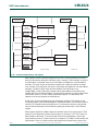 333
333
-
 334
334
-
 335
335
-
 336
336
-
 337
337
-
 338
338
-
 339
339
-
 340
340
-
 341
341
-
 342
342
-
 343
343
-
 344
344
-
 345
345
-
 346
346
-
 347
347
-
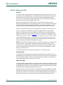 348
348
-
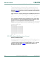 349
349
-
 350
350
-
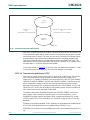 351
351
-
 352
352
-
 353
353
-
 354
354
-
 355
355
-
 356
356
-
 357
357
-
 358
358
-
 359
359
-
 360
360
-
 361
361
-
 362
362
-
 363
363
-
 364
364
-
 365
365
-
 366
366
-
 367
367
-
 368
368
-
 369
369
-
 370
370
-
 371
371
-
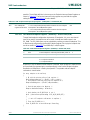 372
372
-
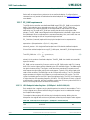 373
373
-
 374
374
-
 375
375
-
 376
376
-
 377
377
-
 378
378
-
 379
379
-
 380
380
-
 381
381
-
 382
382
-
 383
383
-
 384
384
-
 385
385
-
 386
386
-
 387
387
-
 388
388
-
 389
389
-
 390
390
-
 391
391
-
 392
392
-
 393
393
-
 394
394
-
 395
395
-
 396
396
-
 397
397
-
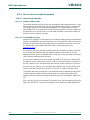 398
398
-
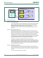 399
399
-
 400
400
-
 401
401
-
 402
402
-
 403
403
-
 404
404
-
 405
405
-
 406
406
-
 407
407
-
 408
408
-
 409
409
-
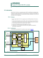 410
410
-
 411
411
-
 412
412
-
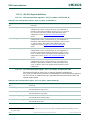 413
413
-
 414
414
-
 415
415
-
 416
416
-
 417
417
-
 418
418
-
 419
419
-
 420
420
-
 421
421
-
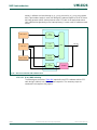 422
422
-
 423
423
-
 424
424
-
 425
425
-
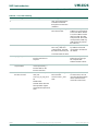 426
426
-
 427
427
-
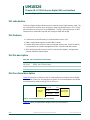 428
428
-
 429
429
-
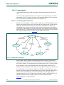 430
430
-
 431
431
-
 432
432
-
 433
433
-
 434
434
-
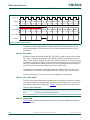 435
435
-
 436
436
-
 437
437
-
 438
438
-
 439
439
-
 440
440
-
 441
441
-
 442
442
-
 443
443
-
 444
444
-
 445
445
-
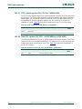 446
446
-
 447
447
-
 448
448
-
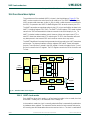 449
449
-
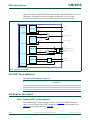 450
450
-
 451
451
-
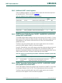 452
452
-
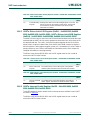 453
453
-
 454
454
-
 455
455
-
 456
456
-
 457
457
-
 458
458
-
 459
459
-
 460
460
-
 461
461
-
 462
462
-
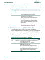 463
463
-
 464
464
-
 465
465
-
 466
466
-
 467
467
-
 468
468
-
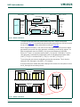 469
469
-
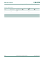 470
470
-
 471
471
-
 472
472
-
 473
473
-
 474
474
-
 475
475
-
 476
476
-
 477
477
-
 478
478
-
 479
479
-
 480
480
-
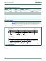 481
481
-
 482
482
-
 483
483
-
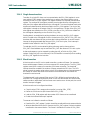 484
484
-
 485
485
-
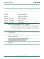 486
486
-
 487
487
-
 488
488
-
 489
489
-
 490
490
-
 491
491
-
 492
492
-
 493
493
-
 494
494
-
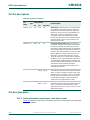 495
495
-
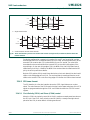 496
496
-
 497
497
-
 498
498
-
 499
499
-
 500
500
-
 501
501
-
 502
502
-
 503
503
-
 504
504
-
 505
505
-
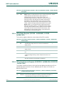 506
506
-
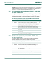 507
507
-
 508
508
-
 509
509
-
 510
510
-
 511
511
-
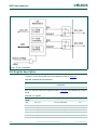 512
512
-
 513
513
-
 514
514
-
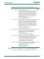 515
515
-
 516
516
-
 517
517
-
 518
518
-
 519
519
-
 520
520
-
 521
521
-
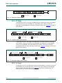 522
522
-
 523
523
-
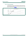 524
524
-
 525
525
-
 526
526
-
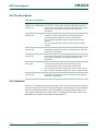 527
527
-
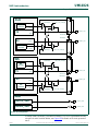 528
528
-
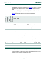 529
529
-
 530
530
-
 531
531
-
 532
532
-
 533
533
-
 534
534
-
 535
535
-
 536
536
-
 537
537
-
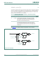 538
538
-
 539
539
-
 540
540
-
 541
541
-
 542
542
-
 543
543
-
 544
544
-
 545
545
-
 546
546
-
 547
547
-
 548
548
-
 549
549
-
 550
550
-
 551
551
-
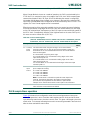 552
552
-
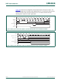 553
553
-
 554
554
-
 555
555
-
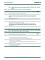 556
556
-
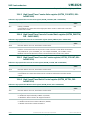 557
557
-
 558
558
-
 559
559
-
 560
560
-
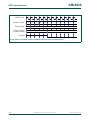 561
561
-
 562
562
-
 563
563
-
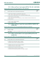 564
564
-
 565
565
-
 566
566
-
 567
567
-
 568
568
-
 569
569
-
 570
570
-
 571
571
-
 572
572
-
 573
573
-
 574
574
-
 575
575
-
 576
576
-
 577
577
-
 578
578
-
 579
579
-
 580
580
-
 581
581
-
 582
582
-
 583
583
-
 584
584
-
 585
585
-
 586
586
-
 587
587
-
 588
588
-
 589
589
-
 590
590
-
 591
591
-
 592
592
-
 593
593
-
 594
594
-
 595
595
-
 596
596
-
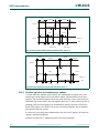 597
597
-
 598
598
-
 599
599
-
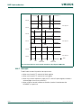 600
600
-
 601
601
-
 602
602
-
 603
603
-
 604
604
-
 605
605
-
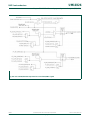 606
606
-
 607
607
-
 608
608
-
 609
609
-
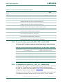 610
610
-
 611
611
-
 612
612
-
 613
613
-
 614
614
-
 615
615
-
 616
616
-
 617
617
-
 618
618
-
 619
619
-
 620
620
-
 621
621
-
 622
622
-
 623
623
-
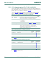 624
624
-
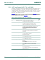 625
625
-
 626
626
-
 627
627
-
 628
628
-
 629
629
-
 630
630
-
 631
631
-
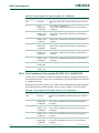 632
632
-
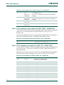 633
633
-
 634
634
-
 635
635
-
 636
636
-
 637
637
-
 638
638
-
 639
639
-
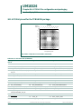 640
640
-
 641
641
-
 642
642
-
 643
643
-
 644
644
-
 645
645
-
 646
646
-
 647
647
-
 648
648
-
 649
649
-
 650
650
-
 651
651
-
 652
652
-
 653
653
-
 654
654
-
 655
655
-
 656
656
-
 657
657
-
 658
658
-
 659
659
-
 660
660
-
 661
661
-
 662
662
-
 663
663
-
 664
664
-
 665
665
-
 666
666
-
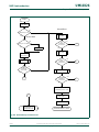 667
667
-
 668
668
-
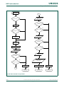 669
669
-
 670
670
-
 671
671
-
 672
672
-
 673
673
-
 674
674
-
 675
675
-
 676
676
-
 677
677
-
 678
678
-
 679
679
-
 680
680
-
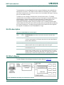 681
681
-
 682
682
-
 683
683
-
 684
684
-
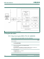 685
685
-
 686
686
-
 687
687
-
 688
688
-
 689
689
-
 690
690
-
 691
691
-
 692
692
-
 693
693
-
 694
694
-
 695
695
-
 696
696
-
 697
697
-
 698
698
-
 699
699
-
 700
700
-
 701
701
-
 702
702
-
 703
703
-
 704
704
-
 705
705
-
 706
706
-
 707
707
-
 708
708
-
 709
709
-
 710
710
-
 711
711
-
 712
712
-
 713
713
-
 714
714
-
 715
715
-
 716
716
-
 717
717
-
 718
718
-
 719
719
-
 720
720
-
 721
721


NXP LPC3220FET296 User guide
- Type
- User guide
- This manual is also suitable for
Ask a question and I''ll find the answer in the document
Finding information in a document is now easier with AI
Related papers

Other documents
-
Silicon Labs EFM32WG Reference guide
-
 PEAK-System PCAN-GPS Microcontroller Operating instructions
-
Digi NS9750 User manual
-
Conceptronic CLMICOTG Datasheet
-
Maverick EP7312 User manual
-
Texas Instruments OMAP5912 Multimedia Processor Display Interface Reference (Rev. B) User guide
-
Intel PXA26X User manual
-
NXP Semiconductors UM10237 User manual
-
Motorola MC68VZ328 User manual
-
Panasonic MN103001G/F01K User manual
