red lion PAX2CHZ/VR Modbus Register Table User manual
- Type
- User manual

REGISTER
ADDRESS
REGISTER NAME
LOW
LIMIT
HIGH
LIMIT
FACTORY
SETTING
ACCESS COMMENTS
FREQUENTLY USED REGISTERS
01 Input Process Value N/A N/A N/A Read 1 = 1 Display Unit
02 Maximum Value -1999 9999 N/A Read 1 = 1 Display Unit
03 Minimum Value -1999 9999 N/A Read 1 = 1 Display Unit
04 Active Setpoint Value SPLO SPHI 0 Read/Write 1 = 1 Display Unit; Limited by setpoint low/high limits
05 Setpoint 1 Value SPLO SPHI 0 Read/Write 1 = 1 Display Unit; Limited by setpoint low/high limits
06 Setpoint 2 Value SPLO SPHI 0 Read/Write 1 = 1 Display Unit; Limited by setpoint low/high limits
07 Setpoint Deviation N/A N/A N/A Read Only 1 = 1 Display Unit
08 Output Power -1000 1000 N/A Read/Write Output Power: Heat/Cool; * writable only in manual mode; 1 = 0.1%
09 Active Proportional Band 0 9999 700 Read/Write 1 = 1 Display Unit
10 Active Integral Time 0 65000 120 Read/Write 1 = 0.1 Second
11 Active Derivative Time 0 9999 30 Read/Write 1 = 0.1 Second
12 Active Power Filter 0 600 10 Read/Write 1 = 0.1 Second
13 Auto-Tune Code 0 4 2 Read/Write
0 = Very Aggressive, 1 = Aggressive, 2 = Default, 3 = Conservative,
4 = Very Conservative
14 Auto-Tune Request 0 1 0 Read/Write
0 = Off, 1 = Invoke Auto-Tune , 2 = Auto-Tune CS1, 3 = Auto-Tune CS2, 4
= Auto-Tune CS3, 5 = Auto-Tune CS4, 6 = Auto-Tune CS5, 7 = Auto-Tune
CS6
15 Auto-Tune Phase 0 4 0 Read 0 = Off, 4 = Last Phase of Auto-Tune
16 Auto-Tune Done 0 1 0 Read 1 = Successful Auto-Tune since last power cycle.
17 Auto-Tune Fail 0 1 0 Read 0 = Off, 1 = Auto-Tune failed
18 Control Mode 0 1 0 Read/Write 0 = Automatic, 1 = Manual Mode
19 Setpoint Selection 0 1 0 Read/Write 0 = Setpoint 1, 1 = Setpoint 2 ... 5 = Setpoint 6
20 Remote/Local Setpoint Selection 0 1 0 Read/Write 0 = Local, 1 = Remote
21 PID Set Selection 0 1 0 Read/Write
0 = PID Set 1 (Pri), 1 = PID Set 2(Alt), 2 = PID Set 3, 3 = PID Set 4, 4 =
PID Set 5, 5 = PID Set 6 , 6 = SPSL, 7 = Auto
22 Disable Integral Action 0 1 0 Read/Write 0 = Enabled, 1 = Disabled
23 Disable Setpoint Ramping 0 1 0 Read/Write 0 = Enabled, 1 = Disabled
24 Setpoint Ramping In Process 0 1 0 Read/Write 0 = Off, 1 = In Process
25 Setpoint Ramp Rate Value -1999 9999 0 Read/Write 1 = 0.1 Setpoint Ramping @ Timebase unit selection
26 Alarm (1-16) Status Register 0 65535 3 Read Bit 15 = A16, Bit 0 = A1
27
PID Stop/Run 0 1 0 Read/Write 0 = Run PID, 1 = Stop PID (Output Power = 0%)
28 User Input Status 0 2 0 Read Bit 1 = User Input 2, Bit 0 = User Input 1
29 Digital Output Status 0 15 N/A Read/Write
Status of Digital Outputs. Bit State: 0 = Off, 1 = On.
Bit 3 = Out1, Bit 2 = Out2, Bit 1 = Out3, Bit 0 = Out4.
Outputs can only be activated/reset with this register when the respective
bits in the Manual Mode Register (MMR) are set.
30 Output Manual Mode Register (MMR) 0 31 0 Read/Write
Bit State: 0 = Auto Mode, 1 = Manual Mode
Bit 4 = DO1, Bit 3 = DO2, Bit 2 = DO3, Bit 1 = DO4, Bit 0 = Linear Output
31 Alarm Reset Register 0 65535 0 Read/Write
Bit State: 1= Reset Alarm, bit is returned to zero following reset processing;
Bit 15 = A16, Bit 0 = A1
PAX2C, PX2FCA0, and PX2FCA1 Modbus Register Tables LP0905F
REVISED 2017-02-27
The following is an example of the necessary query and corresponding response for holding register 2. In this example register 2 is the decimal value 123.
Query: 01 03 00 01 00 01 D5 CA
Response: 01 03 02 00 7B F8 67
Notes:
1. The PAX2C registers can be read as holding (4x) or input (3x) registers.
2. The PAX2C should not be powered down while parameters are being changed. Doing so may corrupt the non-volatile memory resulting in checksum errors.
PAX2C Ver 2.0 Modbus Register Table

REGISTER
ADDRESS
REGISTER NAME
LOW
LIMIT
HIGH
LIMIT
FACTORY
SETTING
ACCESS COMMENTS
32 Analog Output Register (AOR) 0 4095 0 Read/Write
Functional only if Linear Output is in Manual Mode.(MMR bit 0 = 1)
Linear Output Card written to only if Linear Out (MMR bit 0) is set.
33 Active Alarm 1 Value -1999 9999 0 Read/Write Active List (A or B); 1 = 1 Display Unit
34 Active Alarm 2 Value -1999 9999 0 Read/Write Active List (A or B); 1 = 1 Display Unit
35 Active Alarm 3 Value -1999 9999 0 Read/Write Active List (A or B); 1 = 1 Display Unit
36 Active Alarm 4 Value -1999 9999 0 Read/Write Active List (A or B); 1 = 1 Display Unit
37 Active Alarm 5 Value -1999 9999 0 Read/Write Active List (A or B); 1 = 1 Display Unit
38 Active Alarm 6 Value -1999 9999 0 Read/Write Active List (A or B); 1 = 1 Display Unit
39 Active Alarm 7 Value -1999 9999 0 Read/Write Active List (A or B); 1 = 1 Display Unit
40 Active Alarm 8 Value -1999 9999 0 Read/Write Active List (A or B); 1 = 1 Display Unit
41 Active Alarm 9 Value -1999 9999 0 Read/Write Active List (A or B); 1 = 1 Display Unit
42 Active Alarm 10 Value -1999 9999 0 Read/Write Active List (A or B); 1 = 1 Display Unit
43 Active Alarm 11 Value -1999 9999 0 Read/Write Active List (A or B); 1 = 1 Display Unit
44 Active Alarm 12 Value -1999 9999 0 Read/Write Active List (A or B); 1 = 1 Display Unit
45 Active Alarm 13 Value -1999 9999 0 Read/Write Active List (A or B); 1 = 1 Display Unit
46 Active Alarm 14 Value -1999 9999 0 Read/Write Active List (A or B); 1 = 1 Display Unit
47 Active Alarm 15 Value -1999 9999 0 Read/Write Active List (A or B); 1 = 1 Display Unit
48 Active Alarm 16 Value -1999 9999 0 Read/Write Active List (A or B); 1 = 1 Display Unit
49 Active Alarm 1 Band/Dev. Value -1999 9999 0 Read/Write Active List (A or B). Applicable only for Band or Deviation Alarm Action.
50 Active Alarm 2 Band/Dev. Value -1999 9999 0 Read/Write Active List (A or B). Applicable only for Band or Deviation Alarm Action.
51 Active Alarm 3 Band/Dev. Value -1999 9999 0 Read/Write Active List (A or B). Applicable only for Band or Deviation Alarm Action.
52 Active Alarm 4 Band/Dev. Value -1999 9999 0 Read/Write Active List (A or B). Applicable only for Band or Deviation Alarm Action.
53 Active Alarm 5 Band/Dev. Value -1999 9999 0 Read/Write Active List (A or B). Applicable only for Band or Deviation Alarm Action.
54 Active Alarm 6 Band/Dev. Value -1999 9999 0 Read/Write Active List (A or B). Applicable only for Band or Deviation Alarm Action.
55 Active Alarm 7 Band/Dev. Value -1999 9999 0 Read/Write Active List (A or B). Applicable only for Band or Deviation Alarm Action.
56 Active Alarm 8 Band/Dev. Value -1999 9999 0 Read/Write Active List (A or B). Applicable only for Band or Deviation Alarm Action.
57 Active Alarm 9 Band/Dev. Value -1999 9999 0 Read/Write Active List (A or B). Applicable only for Band or Deviation Alarm Action.
58 Active Alarm 10 Band/Dev. Value -1999 9999 0 Read/Write Active List (A or B). Applicable only for Band or Deviation Alarm Action.
59 Active Alarm 11 Band/Dev. Value -1999 9999 0 Read/Write Active List (A or B). Applicable only for Band or Deviation Alarm Action.
60 Active Alarm 12 Band/Dev. Value -1999 9999 0 Read/Write Active List (A or B). Applicable only for Band or Deviation Alarm Action.
61 Active Alarm 13 Band/Dev. Value -1999 9999 0 Read/Write Active List (A or B). Applicable only for Band or Deviation Alarm Action.
62 Active Alarm 14 Band/Dev. Value -1999 9999 0 Read/Write Active List (A or B). Applicable only for Band or Deviation Alarm Action.
63 Active Alarm 15 Band/Dev. Value -1999 9999 0 Read/Write Active List (A or B). Applicable only for Band or Deviation Alarm Action.
64 Active Alarm 16 Band/Dev. Value -1999 9999 0 Read/Write Active List (A or B). Applicable only for Band or Deviation Alarm Action.
65 Remote SP Value -1999 9999 0 Read Only
66 Prole Operating Status 0 5 0 Read/Write
0 = Prole Control Mode Off; Unit will control to active setpoint, 1 = End
Prole; Control per prole end action, 2 = Pause, 3 = Error Delay (status
only), 4 = Run/Resume/Start, 5 = Advance Prole Segment
67 Active Prole 1 16 1 Read (0 = Stop, 1-16 = Current Prole)
68 Active Segment 1 20 1 Read (0 = Stop, 1-20 = Current Segment)
69 Prole Segment Type 0 1 0 Read 0 = Ramp, 1 = Hold
70 Active Prole Cycle Count Remaining 0 250 0 Read/Write 0-250; If Cycle Count is 0 unit is congured for continuous cycling
71 Active Prole Segment Time Remaining (Hi Word)
0 9999 N/A Read/Write
1 = 0.1 Minute; Can make temporary change on the y, however, if Active
Prole Segment’s Time resolution is in minutes, the least signicant
decade is ignored (i.e., 38 = 30 minutes)
72 Active Prole Segment Time Remaining (Lo Word)
73 Prole Event Status 0 15 0 Read/Write Bit 3 = Event 4, Bit 2 = Event 3, Bit 1 = Event 2; Bit 0 = Event 1

REGISTER
ADDRESS
REGISTER NAME
LOW
LIMIT
HIGH
LIMIT
FACTORY
SETTING
ACCESS COMMENTS
INPUT PARAMETERS SEE INPUT MODULE FOR PARAMETER DESCRIPTIONS
Analog Input Parameters
101 Input Range 0 26 16 Read/Write
0 = 250µA 5 = 250mV 11 = 100Ω 17 = TC-K 23 = RTD 385
1 = 2.5mA 6 = 2V 12 = 1KΩ 18 = TC-R 24 = RTD 392
2 = 25mA 7 = 10V 13 = 10KΩ 19 = TC-S 25 = RTD 672
3 = 250mA 8 = 25V 14 = TC-T 20 = TC-B 26 = RTD 427
4 = 2A 9 = 100V 15 = TC-E 21 = TC-N
10 = 200V 16 = TC-J 22 = TC-C
102 Square Root Linearization 0 1 0 Read/Write 0 = No, 1 = Yes (Valid on Process Inputs)
103 Temperature Scale (TC or RTD only) 0 1 1 Read/Write 0 = °C, 1 = °F
104 Ice Point Compensation (TC only) 0 1 1 Read/Write 0 = Off, 1 = On
105 ADC Conversion Rate (samples/sec) 0 5 2 Read/Write 0 = 5, 1 = 10, 2 = 20, 3 = 40, 4 = 80, 5 = 160
106 Decimal Point 0 3 1 Read/Write 0 = 0, 1 = 0.0, 2 = 0.00, 3 = 0.000
107 Rounding Factor 0 6 0 Read/Write 0 = 1, 1 = 2, 2 = 5, 3 = 10, 4 = 20, 5 = 50, 6 = 100
108 Input Offset Value -1999 9999 0 Read/Write 1 = 1 Display Unit
109 Digital Input Filter 0 250 10 Read/Write 1 = 0.1 Second
110 Input Scaling Points in List Function 0 1 0 Read/Write 0 = No, 1 = Yes
111 Display Input Units 0 1 1 Read/Write 0 = No, 1 = Yes
112 Input Units Character 1 0 57 0 Read/Write
Label Mnemonic Characters
0 = 9 = I 18 = Q 27 = Z 36 = 8 45 = m(r) 54 = ]
1 = A 10 = J 19 = R 28 = 0 37 = 9 46 = o 55 = /
2 = b 11 = K 20 = S 29 = 1 38 = a 47 = q 56 = º
3 = C 12 = L 21 = t 30 = 2 39 = c 48 = r 57 = _
4 = d 13 = M(l) 22 = U 31 = 3 40 = e 49 = u
5 = E 14 = M(r) 23 = V 32 = 4 41 = g 50 = w(r)
6 = F 15 = N 24 = W(l) 33 = 5 42 = h 51 = -
7 = G 16 = O 25 = W(r) 34 = 6 43 = i 52 = =
8 = H 17 = P 26 = Y 35 = 7 44 = n 53 = [
113 Input Units Character 2 56 Read/Write See Input Units Character 1
114 Input Units Character 3 6 Read/Write See Input Units Character 1
User Input / Function Keys
151 User Input Active State 0 1 0 Read/Write 0 = Active Low, 1 = Active High
152 User Input 1 Action 0 29* 0 Read/Write
0 = NONE 7 = SPrP 14 = dLEV 21 = PrrS 28 = NA-1
1 = PLOC 8 = d-HI 15 = dISP 22 = PrrH 29 = NA-2
2 = ILOC 9 = r-HI 16 = LISt 23 = PStr 30+ = FC Functions
3 = trnF 10 = d-Lo 17 = Prnt 24 = Adnc
4 = SPSL 11 = r-Lo 18 = RnSt 25 = PAUS
5 = RSPt 12 = r-HL 19 = PlrS 26 = PEnd
6 = PSEL 13 = r-AL 20 = PlrH 27 = r-Ev
153 User Input 1 Alarm Mask 0 65535 0 Read/Write
Bit 0 = A1 Bit 4 = A5 Bit 8 = A9 Bit 12 = A13
Bit 1 = A2 Bit 5 = A6 Bit 9 = A10 Bit 13 = A14
Bit 2 = A3 Bit 6 = A7 Bit 10 = A11 Bit 14 = A15
Bit 3 = A4 Bit 7 = A8 Bit 11 = A12 Bit 15 = A16
154 User Input 2 Action 0 29* 0 Read/Write Same as User Input 1 Action
155 User Input 2 Alarm Mask 0 65535 0 Read/Write Same as User Input 1 Alarm Mask
156 User F1 Key Action 0 26* 0 Read/Write
0 = NONE 6 = SPrP 12 = dISP 18 = PrrS 24 = r-Ev
1 = ILOC 7 = r-HI 13 = LISt 19 = PrrH 25 = NA-1
2 = trnF 8 = r-Lo 14 = Prnt 20 = PStr 26 = NA-2
3 = SPSL 9 = r-HL 15 = RnSt 21 = Adnc 27+ = FC Functions
4 = RSPt 10 = r-AL 16 = PlrS 22 = PAUS
5 = PSEL 11 = dLEV 17 = PlrH 23 = PEnd
157 User F1 Key Alarm Mask 0 65535 0 Read/Write Same as User Input 1 Alarm Mask

REGISTER
ADDRESS
REGISTER NAME
LOW
LIMIT
HIGH
LIMIT
FACTORY
SETTING
ACCESS COMMENTS
158 User F2 Key Action 0 26* 0 Read/Write Same as User F1 Key Action
159 User F2 Key Alarm Mask 0 65535 0 Read/Write Same as User Input 1 Alarm Mask
160 User F1 Second Action 0 26* 0 Read/Write Same as User F1 Key Action
161 User F1 Second Alarm Mask 0 65535 0 Read/Write Same as User Input 1 Alarm Mask
162 User F2 Second Action 0 26* 0 Read/Write Same as User F1 Key Action
163 User F2 Second Alarm Mask 0 65535 0 Read/Write Same as User Input 1 Alarm Mask
Advanced Input Parameters
List A List B Input Scaling Points Parameters
171 211 Number of Scaling Points 2 16 2 Read/Write Number of Linearization Scaling Points
172 212 Reserved N/A N/A N/A N/A
173 213 Scaling Pt. 1 Input Value -1999 9999 0 Read/Write 1 = 0.001
174 214 Scaling Pt. 1 Display Value -1999 9999 0 Read/Write 1 = 1 Display Unit
175 215 Scaling Pt. 2 Input Value -1999 9999 1000 Read/Write 1 = 0.001
176 216 Scaling Pt. 2 Display Value -1999 9999 1000 Read/Write 1 = 1 Display Unit
177 thru
202
217 thru
242
Scaling Pts. 3 thru 15 Values -1999 9999 0 Read/Write
Registers 40177-40202 and 40217-40242 hold values for Scaling Points 3
thru 15, and follow the same ordering as Scaling Point 1.
203 243 Scaling Pt. 16 Input Value -1999 9999 0 Read/Write 1 = 0.001
204 244 Scaling Pt. 16 Display Value -1999 9999 0 Read/Write 1 = 1 Display Unit
OUTPUT PARAMETERS
251 Output 1 Assignment 0 23* 1 Read/Write
0 = NONE 7 = RSPt 14 = PHLd 21 = PEv4
1 = HEAt 8 = ILOC 15 = PAUS 22 = NA-1
2 = COOL 9 = tunE 16 = PErb 23 = NA-2
3 = ALr 10 = tndn 17 = PErt 24+ = FlexCard
4 = MAN 11 = tnFL 18 = PEv1 Assignments
5 = SPSL 12 = PCtL 19 = PEv2
6 = SPrP 13 = Prun 20 = PEv3
252 Output 1 Logic/Alarm Logic Mode 0 2 0 Read/Write
If Out Assignment ≠ ALr; 0 = NOR, 1 = REV
If Output Assignment = ALr; 0 = SINGLE, 1 = AND, 2 = OR
253 Output 1 Alarm Mask 0 65535 0 Read/Write
Bit 0 = A1 Bit 4 = A5 Bit 8 = A9 Bit 12 = A13
Bit 1 = A2 Bit 5 = A6 Bit 9 = A10 Bit 13 = A14
Bit 2 = A3 Bit 6 = A7 Bit 10 = A11 Bit 14 = A15
Bit 3 = A4 Bit 7 = A8 Bit 11 = A12 Bit 15 = A16
254 Output 1 Cycle Time 0 600 20 Read/Write 1 = 0.1 Second
255 Output 2 Assignment 0 23* 0 Read/Write Same as Output 1 Assignment
256 Output 2 Logic/Alarm Logic Mode 0 2 0 Read/Write Same as Output 1 Logic/Alarm Logic Mode
257 Output 2 Alarm Mask 0 65535 0 Read/Write Same as Output 1 Alarm Mask
258 Output 2 Cycle Time 0 600 20 Read/Write 1 = 0.1 Second
259 Output 3 Assignment 0 23* 0 Read/Write Same as Output 1 Assignment
260 Output 3 Logic/Alarm Logic Mode 0 2 0 Read/Write Same as Output 1 Logic/Alarm Logic Mode
261 Output 3 Alarm Mask 0 65535 0 Read/Write Same as Output 1 Alarm Mask
262 Output 3 Cycle Time 0 600 20 Read/Write 1 = 0.1 Second
263 Output 4 Assignment 0 23* 0 Read/Write Same as Output 1 Assignment
264 Output 4 Logic/Alarm Logic Mode 0 2 0 Read/Write Same as Output 1 Logic/Alarm Logic Mode
265 Output 4 Alarm Mask 0 65535 0 Read/Write Same as Output 1 Alarm Mask
266 Output 4 Cycle Time 0 600 20 Read/Write 1 = 0.1 Second
Analog Output
271 Non-Linear Analog Output Scaling 0 1 0 Read/Write 0 = No, 1 = Yes (Use Non-Linear Analog Output Scaling Parameters)
272 Type 0 2 1 Read/Write 0 = 0-20 mA, 1 = 4-20 mA, 2 = 0-10 V
273 Assignment 0 6* 0 Read/Write
0 = NONE, 1 = PV, 2 = HI, 3 = LO, 4 = OP, 5 = SP (Active), 6 = dEv,
7+ = FlexCard Assignments
274 Analog Low Scale Value -1999 9999 0 Read/Write Display value that corresponds with 0 V, 0 mA or 4 mA output
275 Analog High Scale Value -1999 9999 1000 Read/Write Display value that corresponds with 10 V or 20 mA output

REGISTER
ADDRESS
REGISTER NAME
LOW
LIMIT
HIGH
LIMIT
FACTORY
SETTING
ACCESS COMMENTS
276 Update time 0 100 0 Read/Write 0 = Max update rate, 1 = 0.1 Second
277 Probe Failure Action (TC or RTD only) 0 1 0 Read/Write 0 = Low Scale, 1 = High Scale (only applies for TC or RTD input)
Non-Linear Analog Output Scaling
List A List B Analog Output Scaling Point Parameters
1721 1761 Number of Scaling Points 2 16 2 Read/Write Number of Linearization Scaling Points
1722 1762 Reserved N/A N/A N/A N/A
1723 1763 Output Value for Scaling Point 1 0 2000 0 Read/Write 1 = 0.01
1724 1764 Parameter Value for Scaling Point 1 -1999 9999 0 Read/Write 1 = 1 Analog Output Assignment value unit
1725 to
1754
1765 to
1794
Scaling Pts. 2 thru 16 Values
Registers 41725-41754 and 41765-41794 hold values for Scaling Points 2
thru 16, and follow the same ordering as Scaling Point 1.
DISPLAY CONFIGURATION PARAMETERS
General
281 Display Intensity Level 0 4 4 Read/Write 0 = Min.(off), 4 = Max.
282 Display Contrast Level 0 15 5 Read/Write
283 Display Update (readings per second) 0 4 1 Read/Write 0 = 1, 1 = 2, 2 = 5, 3 = 10, 4 = 20
284 Conguration Mode 0 1 1 Read/Write 0 = Advanced, 1 = Basic (Caution: Affects other parameters, see manual)
Hardware Label Mnemonic
Adds a user programmable hardware label mnemonic to all PAX2C
line 2 parameters in main, parameter, and hidden display loops when
programmed (non-blank).
286 Hardware Label Character 1 0 57 0 Read/Write
Label Mnemonic Characters
0 = 9 = I 18 = Q 27 = Z 36 = 8 45 = m(r) 54 = ]
1 = A 10 = J 19 = R 28 = 0 37 = 9 46 = o 55 = /
2 = b 11 = K 20 = S 29 = 1 38 = a 47 = q 56 = º
3 = C 12 = L 21 = t 30 = 2 39 = c 48 = r 57 = _
4 = d 13 = M(l) 22 = U 31 = 3 40 = e 49 = u
5 = E 14 = M(r) 23 = V 32 = 4 41 = g 50 = w(r)
6 = F 15 = N 24 = W(l) 33 = 5 42 = h 51 = -
7 = G 16 = O 25 = W(r) 34 = 6 43 = i 52 = =
8 = H 17 = P 26 = Y 35 = 7 44 = n 53 = [
287 Hardware Label Character 2 0 57 0 Read/Write See Hardware Label Character 1
288 Hardware Label Character 3 0 57 0 Read/Write See Hardware Label Character 1
Line 1
291 Line 1 Display Assignment 0 3* 1 Read/Write 0 = NONE, 1 = PV, 2 = HI, 3 = LO, 4+ = FlexCard Assignments
292 Line 1 Default Display Color 0 2 2 Read/Write 0 = Grn, 1 = OrNG, 2 = rEd
293 Deprecated See Registers 111-114 for Input Units programming
294 Deprecated
295 Deprecated
296 Deprecated
297 Line 1 Bargraph Assignment 0 3* 1 Read/Write 0 = NONE, 1 = OP, 2 = dEv, 3 = SP, 4+ = FlexCard Assignments
298 Line 1 Bargraph Low Scale Value 0 9999 0 Read/Write
299 Line 1 Bargraph High Scale Value 0 9999 1000 Read/Write
300 Line 1 Green Backlight Assignment 0 25* 0 Read/Write
0 = NONE 5 = ALr 10 = ILOC 15 = Prun 20 = PEv1 25 = NA-2
1 = Out1 6 = MAN 11 = tunE 16 = PHLd 21 = PEv2 26+ = FlexCard
2 = Out2 7 = SPSL 12 = tndn 17 = PAUS 22 = PEv3 Assignments
3 = Out3 8 = SPrP 13 = tnFL 18 = PErb 23 = PEv4
4 = Out4 9 = RSPt 14 = PCtL 19 = PErt 24 = NA-1
301 Line 1 Green Backlight Alarm Logic Mode 0 2 0 Read/Write 0 = SINGLE, 1 = AND, 2 = OR
302 Line 1 Green Backlight Alarm Mask 0 65535 0 Read/Write
Bit 0 = A1 Bit 4 = A5 Bit 8 = A9 Bit 12 = A13
Bit 1 = A2 Bit 5 = A6 Bit 9 = A10 Bit 13 = A14
Bit 2 = A3 Bit 6 = A7 Bit 10 = A11 Bit 14 = A15
Bit 3 = A4 Bit 7 = A8 Bit 11 = A12 Bit 15 = A16
303 Line 1 Orange Backlight Assignment 0 25* 0 Read/Write Same as Line 1 Green Backlight Assignment

REGISTER
ADDRESS
REGISTER NAME
LOW
LIMIT
HIGH
LIMIT
FACTORY
SETTING
ACCESS COMMENTS
304 Line 1 Orange Backlight Alarm Logic Mode 0 2 0 Read/Write 0 = SINGLE, 1 = AND, 2 = OR
305 Line 1 Orange Backlight Alarm Mask 0 65535 0 Read/Write Same as Line 1 Green Backlight Alarm Mask
306 Line 1 Red Backlight Assignment 0 25* 0 Read/Write Same as Line 1 Green Backlight Assignment
307 Line 1 Red Backlight Alarm Logic Mode 0 2 0 Read/Write 0 = SINGLE, 1 = AND, 2 = OR
308 Line 1 Red Backlight Alarm Mask 0 65535 0 Read/Write Same as Line 1 Green Backlight Alarm Mask
309 Line 1 Green-Orange Backlight Assignment 0 25* 0 Read/Write Same as Line 1 Green Backlight Assignment
310 Line 1 Green-Orange Backlight Alarm Logic Mode 0 2 0 Read/Write 0 = SINGLE, 1 = AND, 2 = OR
311 Line 1 Green-Orange Backlight Alarm Mask 0 65535 0 Read/Write Same as Line 1 Green Backlight Alarm Mask
312 Line 1 Red-Orange Backlight Assignment 0 25* 0 Read/Write Same as Line 1 Green Backlight Assignment
313 Line 1 Red-Orange Backlight Alarm Logic Mode 0 2 0 Read/Write 0 = SINGLE, 1 = AND, 2 = OR
314 Line 1 Red-Orange Backlight Alarm Mask 0 65535 0 Read/Write Same as Line 1 Green Backlight Alarm Mask
315 Line 1 Red-Green Backlight Assignment 0 25* 0 Read/Write Same as Line 1 Green Backlight Assignment
316 Line 1 Red-Green Backlight Alarm Logic Mode 0 2 0 Read/Write 0 = SINGLE, 1 = AND, 2 = OR
317 Line 1 Red-Green Backlight Alarm Mask 0 65535 0 Read/Write Same as Line 1 Green Backlight Alarm Mask
Line 2
331 Line 2 Default Display Color 0 2 0 Read/Write 0 = Grn, 1 = OrNG, 2 = rEd
332 Deprecated See registers 111-114 for Input Unit's programming
333 Deprecated See registers 111-114 for Input Unit's programming
334 Deprecated See registers 111-114 for Input Unit's programming
335 Deprecated See registers 111-114 for Input Unit's programming
336 Line 2 Bargraph Assignment 0 6* 2 Read/Write
0 = NONE, 1 = OP, 2 = dEv, 3 = SP, 4 = OP ANy, 5 = dEv ANy,
6 = SP ANy, 7+ = FlexCard Assignments
337 Line 2 Bargraph Low Scale Value 0 9999 0 Read/Write
338 Line 2 Bargraph High Scale Value 0 9999 100 Read/Write
339 Line 2 Green Backlight Assignment 0 25* 0 Read/Write
0 = NONE 5 = ALr 10 = ILOC 15 = Prun 20 = PEv1 25 = NA-2
1 = Out1 6 = MAN 11 = tunE 16 = PHLd 21 = PEv2 26+ = FlexCard
2 = Out2 7 = SPSL 12 = tndn 17 = PAUS 22 = PEv3 Assignments
3 = Out3 8 = SPrP 13 = tnFL 18 = PErb 23 = PEv4
4 = Out4 9 = RSPt 14 = PCtL 19 = PErt 24 = NA-1
340 Line 2 Green Backlight Alarm Logic Mode 0 2 0 Read/Write 0 = SINGLE, 1 = AND, 2 = OR
341 Line 2 Green Backlight Alarm Mask 0 65535 0 Read/Write
Bit 0 = A1 Bit 4 = A5 Bit 8 = A9 Bit 12 = A13
Bit 1 = A2 Bit 5 = A6 Bit 9 = A10 Bit 13 = A14
Bit 2 = A3 Bit 6 = A7 Bit 10 = A11 Bit 14 = A15
Bit 3 = A4 Bit 7 = A8 Bit 11 = A12 Bit 15 = A16
342 Line 2 Orange Backlight Assignment 0 25* 0 Read/Write Same as Line 2 Green Backlight Assignment
343 Line 2 Orange Backlight Alarm Logic Mode 0 2 0 Read/Write 0 = SINGLE, 1 = AND, 2 = OR
344 Line 2 Orange Backlight Alarm Mask 0 65535 0 Read/Write Same as Line 2 Green Backlight Alarm Mask
345 Line 2 Red Backlight Assignment 0 25* 0 Read/Write Same as Line 2 Green Backlight Assignment
346 Line 2 Red Backlight Alarm Logic Mode 0 2 0 Read/Write 0 = SINGLE, 1 = AND, 2 = OR
347 Line 2 Red Backlight Alarm Mask 0 65535 0 Read/Write Same as Line 2 Green Backlight Alarm Mask
348 Line 2 Green-Orange Backlight Assignment 0 25* 0 Read/Write Same as Line 2 Green Backlight Assignment
349 Line 2 Green-Orange Backlight Alarm Logic Mode 0 2 0 Read/Write 0 = SINGLE, 1 = AND, 2 = OR
350 Line 2 Green-Orange Backlight Alarm Mask 0 65535 0 Read/Write Same as Line 2 Green Backlight Alarm Mask
351 Line 2 Red-Orange Backlight Assignment 0 25* 0 Read/Write Same as Line 2 Green Backlight Assignment
352 Line 2 Red-Orange Backlight Alarm Logic Mode 0 2 0 Read/Write 0 = SINGLE, 1 = AND, 2 = OR
353 Line 2 Red-Orange Backlight Alarm Mask 0 65535 0 Read/Write Same as Line 2 Green Backlight Alarm Mask
354 Line 2 Red-Green Backlight Assignment 0 25* 0 Read/Write Same as Line 2 Green Backlight Assignment
355 Line 2 Red-Green Backlight Alarm Logic Mode 0 2 0 Read/Write 0 = SINGLE, 1 = AND, 2 = OR
356 Line 2 Red-Green Backlight Alarm Mask 0 65535 0 Read/Write Same as Line 2 Green Backlight Alarm Mask

REGISTER
ADDRESS
REGISTER NAME
LOW
LIMIT
HIGH
LIMIT
FACTORY
SETTING
ACCESS COMMENTS
Universal Annunciator 1
361 UA 1 Default Display Color 0 2 0 Read/Write 0 = Grn, 1 = OrNG, 2 = rEd
362 UA 1 Units Mnemonic 0 1 1 Read/Write 0 = Off, 1 = On
363 UA 1 Units Digit 1 (Left) 0 57 16 Read/Write
0 = 9 = I 18 = Q 27 = Z 36 = 8 45 = m(r) 54 = ]
1 = A 10 = J 19 = R 28 = 0 37 = 9 46 = o 55 = /
2 = b 11 = K 20 = S 29 = 1 38 = a 47 = q 56 = º
3 = C 12 = L 21 = t 30 = 2 39 = c 48 = r 57 = _
4 = d 13 = M(l) 22 = U 31 = 3 40 = e 49 = u
5 = E 14 = M(r) 23 = V 32 = 4 41 = g 50 = w(r)
6 = F 15 = N 24 = W(l) 33 = 5 42 = h 51 = -
7 = G 16 = O 25 = W(r) 34 = 6 43 = i 52 = =
8 = H 17 = P 26 = Y 35 = 7 44 = n 53 = [
364 UA 1 Units Digit 2 (Right) 0 57 29 Read/Write
365 UA 1 Units Logic Mode (Active) 0 2 0 Read/Write 0 = nor, 1 = rEv, 2 = FLSh
366 UA 1 Units Assignment 0 25* 1 Read/Write
0 = NONE 5 = ALr 10 = ILOC 15 = Prun 20 = PEv1 25 = NA-2
1 = Out1 6 = MAN 11 = tunE 16 = PHLd 21 = PEv2 26+ = FlexCard
2 = Out2 7 = SPSL 12 = tndn 17 = PAUS 22 = PEv3 Assignments
3 = Out3 8 = SPrP 13 = tnFL 18 = PErb 23 = PEv4
4 = Out4 9 = RSPt 14 = PCtL 19 = PErt 24 = NA-1
367 UA 1 Assignment Alarm Logic Mode 0 2 0 Read/Write 0 = SINGLE, 1 = AND, 2 = OR
368 UA 1 Assignment Alarm Mask 0 65535 0 Read/Write
Bit 0 = A1 Bit 4 = A5 Bit 8 = A9 Bit 12 = A13
Bit 1 = A2 Bit 5 = A6 Bit 9 = A10 Bit 13 = A14
Bit 2 = A3 Bit 6 = A7 Bit 10 = A11 Bit 14 = A15
Bit 3 = A4 Bit 7 = A8 Bit 11 = A12 Bit 15 = A16
369 UA 1 Green Backlight Assignment 0 25* 0 Read/Write Same as UA 1 Units Assignment
370 UA 1 Green Backlight Alarm Logic Mode 0 2 0 Read/Write 0 = SINGLE, 1 = AND, 2 = OR
371 UA 1 Green Backlight Alarm Mask 0 65535 0 Read/Write Same as UA 1 Assignment Alarm Mask
372 UA 1 Orange Backlight Assignment 0 25* 0 Read/Write Same as UA 1 Units Assignment
373 UA 1 Orange Backlight Alarm Logic Mode 0 2 0 Read/Write 0 = SINGLE, 1 = AND, 2 = OR
374 UA 1 Orange Backlight Alarm Mask 0 65535 0 Read/Write Same as UA 1 Assignment Alarm Mask
375 UA 1 Red Backlight Assignment 0 25* 0 Read/Write Same as UA 1 Units Assignment
376 UA 1 Red Backlight Alarm Logic Mode 0 2 0 Read/Write 0 = SINGLE, 1 = AND, 2 = OR
377 UA 1 Red Backlight Alarm Mask 0 65535 0 Read/Write Same as UA 1 Assignment Alarm Mask
378 UA 1 Green-Orange Backlight Assignment 0 25* 0 Read/Write Same as UA 1 Units Assignment
379 UA 1 Green-Orange Backlight Alarm Logic Mode 0 2 0 Read/Write 0 = SINGLE, 1 = AND, 2 = OR
380 UA 1 Green-Orange Backlight Alarm Mask 0 65535 0 Read/Write Same as UA 1 Assignment Alarm Mask
381 UA 1 Red-Orange Backlight Assignment 0 25* 0 Read/Write Same as UA 1 Units Assignment
382 UA 1 Red-Orange Backlight Alarm Logic Mode 0 2 0 Read/Write 0 = SINGLE, 1 = AND, 2 = OR
383 UA 1 Red-Orange Backlight Alarm Mask 0 65535 0 Read/Write Same as UA 1 Assignment Alarm Mask
384 UA 1 Red-Green Backlight Assignment 0 25* 0 Read/Write Same as UA 1 Units Assignment
385 UA 1 Red-Green Backlight Alarm Logic Mode 0 2 0 Read/Write 0 = SINGLE, 1 = AND, 2 = OR
386 UA 1 Red-Green Backlight Alarm Mask 0 65535 0 Read/Write Same as UA 1 Assignment Alarm Mask
Universal Annunciator 2
391 UA 2 Default Display Color 0 2 0 Read/Write 0 = Grn, 1 = OrNG, 2 = rEd
392 UA 2 Units Mnemonic 0 1 1 Read/Write 0 = Off, 1 = On
393 UA 2 Units Digit 1 (Left) 0 57 1 Read/Write Same as UA1 Units Selection
394 UA 2 Units Digit 2 (Right) 0 57 29 Read/Write
395 UA 2 Units Logic Mode (Active) 0 2 0 Read/Write 0 = nor, 1 = rEv, 2 = FLSh
396 UA 2 Units Assignment 0 25* 5 Read/Write
0 = NONE 5 = ALr 10 = ILOC 15 = Prun 20 = PEv1 25 = NA-2
1 = Out1 6 = MAN 11 = tunE 16 = PHLd 21 = PEv2 26+ = FlexCard
2 = Out2 7 = SPSL 12 = tndn 17 = PAUS 22 = PEv3 Assignments
3 = Out3 8 = SPrP 13 = tnFL 18 = PErb 23 = PEv4
4 = Out4 9 = RSPt 14 = PCtL 19 = PErt 24 = NA-1

REGISTER
ADDRESS
REGISTER NAME
LOW
LIMIT
HIGH
LIMIT
FACTORY
SETTING
ACCESS COMMENTS
397 UA 2 Assignment Alarm Logic Mode 0 2 0 Read/Write 0 = SINGLE, 1 = AND, 2 = OR
398 UA 2 Assignment Alarm Mask 0 65535 1 Read/Write
Bit 0 = A1 Bit 4 = A5 Bit 8 = A9 Bit 12 = A13
Bit 1 = A2 Bit 5 = A6 Bit 9 = A10 Bit 13 = A14
Bit 2 = A3 Bit 6 = A7 Bit 10 = A11 Bit 14 = A15
Bit 3 = A4 Bit 7 = A8 Bit 11 = A12 Bit 15 = A16
399 UA 2 Green Backlight Assignment 0 25* 0 Read/Write Same as UA 2 Units Assignment
400 UA 2 Green Backlight Alarm Logic Mode 0 2 0 Read/Write 0 = SINGLE, 1 = AND, 2 = OR
401 UA 2 Green Backlight Alarm Mask 0 65535 0 Read/Write Same as UA 2 Assignment Alarm Mask
402 UA 2 Orange Backlight Assignment 0 25* 0 Read/Write Same as UA 2 Units Assignment
403 UA 2 Orange Backlight Alarm Logic Mode 0 2 0 Read/Write 0 = SINGLE, 1 = AND, 2 = OR
404 UA 2 Orange Backlight Alarm Mask 0 65535 0 Read/Write Same as UA 2 Assignment Alarm Mask
405 UA 2 Red Backlight Assignment 0 25* 5 Read/Write Same as UA 2 Units Assignment
406 UA 2 Red Backlight Alarm Logic Mode 0 2 0 Read/Write 0 = SINGLE, 1 = AND, 2 = OR
407 UA 2 Red Backlight Alarm Mask 0 65535 1 Read/Write Same as UA 2 Assignment Alarm Mask
408 UA 2 Green-Orange Backlight Assignment 0 25* 0 Read/Write Same as UA 2 Units Assignment
409 UA 2 Green-Orange Backlight Alarm Logic Mode 0 2 0 Read/Write 0 = SINGLE, 1 = AND, 2 = OR
410 UA 2 Green-Orange Backlight Alarm Mask 0 65535 0 Read/Write Same as UA 2 Assignment Alarm Mask
411 UA 2 Red-Orange Backlight Assignment 0 25* 0 Read/Write Same as UA 2 Units Assignment
412 UA 2 Red-Orange Backlight Alarm Logic Mode 0 2 0 Read/Write 0 = SINGLE, 1 = AND, 2 = OR
413 UA 2 Red-Orange Backlight Alarm Mask 0 65535 0 Read/Write Same as UA 2 Assignment Alarm Mask
414 UA 2 Red-Green Backlight Assignment 0 25* 0 Read/Write Same as UA 2 Units Assignment
415 UA 2 Red-Green Backlight Alarm Logic Mode 0 2 0 Read/Write 0 = SINGLE, 1 = AND, 2 = OR
416 UA 2 Red-Green Backlight Alarm Mask 0 65535 0 Read/Write Same as UA 2 Assignment Alarm Mask
Universal Annunciator 3
421 UA 3 Default Display Color 0 2 0 Read/Write 0 = Grn, 1 = OrNG, 2 = rEd
422 UA 3 Units Mnemonic 0 1 1 Read/Write 0 = Off, 1 = On
423 UA 3 Units Digit 1 (Left) 0 57 1 Read/Write Same as UA1 Units Selection
424 UA 3 Units Digit 2 (Right) 0 57 30 Read/Write
425 UA 3 Units Logic Mode (Active) 0 2 0 Read/Write 0 = nor, 1 = rEv, 2 = FLSh
426 UA 3 Units Assignment 0 25* 5 Read/Write
0 = NONE 5 = ALr 10 = ILOC 15 = Prun 20 = PEv1 25 = NA-2
1 = Out1 6 = MAN 11 = tunE 16 = PHLd 21 = PEv2 26+ = FlexCard
2 = Out2 7 = SPSL 12 = tndn 17 = PAUS 22 = PEv3 Assignments
3 = Out3 8 = SPrP 13 = tnFL 18 = PErb 23 = PEv4
4 = Out4 9 = RSPt 14 = PCtL 19 = PErt 24 = NA-1
427 UA 3 Assignment Alarm Logic Mode 0 2 0 Read/Write 0 = SINGLE, 1 = AND, 2 = OR
428 UA 3 Assignment Alarm Mask 0 65535 2 Read/Write
Bit 0 = A1 Bit 4 = A5 Bit 8 = A9 Bit 12 = A13
Bit 1 = A2 Bit 5 = A6 Bit 9 = A10 Bit 13 = A14
Bit 2 = A3 Bit 6 = A7 Bit 10 = A11 Bit 14 = A15
Bit 3 = A4 Bit 7 = A8 Bit 11 = A12 Bit 15 = A16
429 UA 3 Green Backlight Assignment 0 25* 0 Read/Write Same as UA 3 Units Assignment
430 UA 3 Green Backlight Alarm Logic Mode 0 2 0 Read/Write 0 = SINGLE, 1 = AND, 2 = OR
431 UA 3 Green Backlight Alarm Mask 0 65535 0 Read/Write Same as UA 3 Assignment Alarm Mask
432 UA 3 Orange Backlight Assignment 0 25* 0 Read/Write Same as UA 3 Units Assignment
433 UA 3 Orange Backlight Alarm Logic Mode 0 2 0 Read/Write 0 = SINGLE, 1 = AND, 2 = OR
434 UA 3 Orange Backlight Alarm Mask 0 65535 0 Read/Write Same as UA 3 Assignment Alarm Mask
435 UA 3 Red Backlight Assignment 0 25** 5 Read/Write Same as UA 3 Units Assignment
436 UA 3 Red Backlight Alarm Logic Mode 0 2 0 Read/Write 0 = SINGLE, 1 = AND, 2 = OR
437 UA 3 Red Backlight Alarm Mask 0 65535 2 Read/Write Same as UA 3 Assignment Alarm Mask
438 UA 3 Green-Orange Backlight Assignment 0 25 0 Read/Write Same as UA 3 Units Assignment
439 UA 3 Green-Orange Backlight Alarm Logic Mode 0 2 0 Read/Write 0 = SINGLE, 1 = AND, 2 = OR
440 UA 3 Green-Orange Backlight Alarm Mask 0 65535 0 Read/Write Same as UA 3 Assignment Alarm Mask
441 UA 3 Red-Orange Backlight Assignment 0 25* 0 Read/Write Same as UA 3 Units Assignment

REGISTER
ADDRESS
REGISTER NAME
LOW
LIMIT
HIGH
LIMIT
FACTORY
SETTING
ACCESS COMMENTS
442 UA 3 Red-Orange Backlight Alarm Logic Mode 0 2 0 Read/Write 0 = SINGLE, 1 = AND, 2 = OR
443 UA 3 Red-Orange Backlight Alarm Mask 0 65535 0 Read/Write Same as UA 3 Assignment Alarm Mask
444 UA 3 Red-Green Backlight Assignment 0 25* 0 Read/Write Same as UA 3 Units Assignment
445 UA 3 Red-Green Backlight Alarm Logic Mode 0 2 0 Read/Write 0 = SINGLE, 1 = AND, 2 = OR
446 UA 3 Red-Green Backlight Alarm Mask 0 65535 0 Read/Write Same as UA 3 Assignment Alarm Mask
Universal Annunciator 4
451 UA 4 Default Display Color 0 2 0 Read/Write 0 = Grn, 1 = OrNG, 2 = rEd
452 UA 4 Units Mnemonic 0 1 0 Read/Write 0 = Off, 1 = On
453 UA 4 Units Digit 1 (Left) 0 57 0 Read/Write Same as UA1 Units Selection
454 UA 4 Units Digit 2 (Right) 0 57 0 Read/Write
455 UA 4 Units Logic Mode (Active) 0 2 0 Read/Write 0 = nor, 1 = rEv, 2 = FLSh
456 UA 4 Units Assignment 0 25* 0 Read/Write
0 = NONE 5 = ALr 10 = ILOC 15 = Prun 20 = PEv1 25 = NA-2
1 = Out1 6 = MAN 11 = tunE 16 = PHLd 21 = PEv2 26+ = FlexCard
2 = Out2 7 = SPSL 12 = tndn 17 = PAUS 22 = PEv3 Assignments
3 = Out3 8 = SPrP 13 = tnFL 18 = PErb 23 = PEv4
4 = Out4 9 = RSPt 14 = PCtL 19 = PErt 24 = NA-1
457 UA 4 Assignment Alarm Logic Mode 0 2 0 Read/Write 0 = SINGLE, 1 = AND, 2 = OR
458 UA 4 Assignment Alarm Mask 0 65535 0 Read/Write
Bit 0 = A1 Bit 4 = A5 Bit 8 = A9 Bit 12 = A13
Bit 1 = A2 Bit 5 = A6 Bit 9 = A10 Bit 13 = A14
Bit 2 = A3 Bit 6 = A7 Bit 10 = A11 Bit 14 = A15
Bit 3 = A4 Bit 7 = A8 Bit 11 = A12 Bit 15 = A16
459 UA 4 Green Backlight Assignment 0 25* 0 Read/Write Same as UA 4 Units Assignment
460 UA 4 Green Backlight Alarm Logic Mode 0 2 0 Read/Write 0 = SINGLE, 1 = AND, 2 = OR
461 UA 4 Green Backlight Alarm Mask 0 65535 0 Read/Write Same as UA 4 Assignment Alarm Mask
462 UA 4 Orange Backlight Assignment 0 25* 0 Read/Write Same as UA 4 Units Assignment
463 UA 4 Orange Backlight Alarm Logic Mode 0 2 0 Read/Write 0 = SINGLE, 1 = AND, 2 = OR
464 UA 4 Orange Backlight Alarm Mask 0 65535 0 Read/Write Same as UA 4 Assignment Alarm Mask
465 UA 4 Red Backlight Assignment 0 25* 0 Read/Write Same as UA 4 Units Assignment
466 UA 4 Red Backlight Alarm Logic Mode 0 2 0 Read/Write 0 = SINGLE, 1 = AND, 2 = OR
467 UA 4 Red Backlight Alarm Mask 0 65535 0 Read/Write Same as UA 4 Assignment Alarm Mask
468 UA 4 Green-Orange Backlight Assignment 0 25* 0 Read/Write Same as UA 4 Units Assignment
469 UA 4 Green-Orange Backlight Alarm Logic Mode 0 2 0 Read/Write 0 = SINGLE, 1 = AND, 2 = OR
470 UA 4 Green-Orange Backlight Alarm Mask 0 65535 0 Read/Write Same as UA 4 Assignment Alarm Mask
471 UA 4 Red-Orange Backlight Assignment 0 25* 0 Read/Write Same as UA 4 Units Assignment
472 UA 4 Red-Orange Backlight Alarm Logic Mode 0 2 0 Read/Write 0 = SINGLE, 1 = AND, 2 = OR
473 UA 4 Red-Orange Backlight Alarm Mask 0 65535 0 Read/Write Same as UA 4 Assignment Alarm Mask
474 UA 4 Red-Green Backlight Assignment 0 25* 0 Read/Write Same as UA 4 Units Assignment
475 UA 4 Red-Green Backlight Alarm Logic Mode 0 2 0 Read/Write 0 = SINGLE, 1 = AND, 2 = OR
476 UA 4 Red-Green Backlight Alarm Mask 0 65535 0 Read/Write Same as UA 4 Assignment Alarm Mask
Mnemonics
501 Mnemonic Default Display Color 0 2 0 Read/Write 0 = Grn, 1 = OrNG, 2 = rEd
502 Mnemonic Green Backlight Assignment 0 25* 0 Read/Write
0 = NONE 5 = ALr 10 = ILOC 15 = Prun 20 = PEv1 25 = NA-2
1 = Out1 6 = MAN 11 = tunE 16 = PHLd 21 = PEv2 26+ = FlexCard
2 = Out2 7 = SPSL 12 = tndn 17 = PAUS 22 = PEv3 Assignments
3 = Out3 8 = SPrP 13 = tnFL 18 = PErb 23 = PEv4
4 = Out4 9 = RSPt 14 = PCtL 19 = PErt 24 = NA-1
503 Mnemonic Green Backlight Alarm Logic Mode 0 2 0 Read/Write 0 = SINGLE, 1 = AND, 2 = OR
504 Mnemonic Green Backlight Alarm Mask 0 65535 0 Read/Write
Bit 0 = A1 Bit 4 = A5 Bit 8 = A9 Bit 12 = A13
Bit 1 = A2 Bit 5 = A6 Bit 9 = A10 Bit 13 = A14
Bit 2 = A3 Bit 6 = A7 Bit 10 = A11 Bit 14 = A15
Bit 3 = A4 Bit 7 = A8 Bit 11 = A12 Bit 15 = A16
505 Mnemonic Orange Backlight Assignment 0 25* 0 Read/Write Same as Mnemonic Green Backlight Assignment

REGISTER
ADDRESS
REGISTER NAME
LOW
LIMIT
HIGH
LIMIT
FACTORY
SETTING
ACCESS COMMENTS
506 Mnemonic Orange Backlight Alarm Logic Mode 0 2 0 Read/Write 0 = SINGLE, 1 = AND, 2 = OR
507 Mnemonic Orange Backlight Alarm Mask 0 65535 0 Read/Write Same as Line 1 Green Backlight Alarm Mask
508 Mnemonic Red Backlight Assignment 0 25* 0 Read/Write Same as Mnemonic Green Backlight Assignment
509 Mnemonic Red Backlight Alarm Logic Mode 0 2 0 Read/Write 0 = SINGLE, 1 = AND, 2 = OR
510 Mnemonic Red Backlight Alarm Mask 0 65535 0 Read/Write Same as Line 1 Green Backlight Alarm Mask
511 Mnemonic Green-Orange Backlight Assignment 0 25* 0 Read/Write Same as Mnemonic Green Backlight Assignment
512
Mnemonic Green-Orange Backlight Alarm Logic
Mode
0 2 0 Read/Write 0 = SINGLE, 1 = AND, 2 = OR
513 Mnemonic Green-Orange Backlight Alarm Mask 0 65535 0 Read/Write Same as Line 1 Green Backlight Alarm Mask
514 Mnemonic Red-Orange Backlight Assignment 0 25* 0 Read/Write Same as Mnemonic Green Backlight Assignment
515
Mnemonic Red-Orange Backlight Alarm Logic
Mode
0 2 0 Read/Write 0 = SINGLE, 1 = AND, 2 = OR
516 Mnemonic Red-Orange Backlight Alarm Mask 0 65535 0 Read/Write Same as Line 1 Green Backlight Alarm Mask
517 Mnemonic Red-Green Backlight Assignment 0 25* 0 Read/Write Same as Mnemonic Green Backlight Assignment
518 Mnemonic Red-Green Backlight Alarm Logic Mode 0 2 0 Read/Write 0 = SINGLE, 1 = AND, 2 = OR
519 Mnemonic Red-Green Backlight Alarm Mask 0 65535 0 Read/Write Same as Line 1 Green Backlight Alarm Mask
Line 2 Prole LOCS
531 Line 2 Prole Control Status Access 0 21 0 Read/Write 0 = LOC; Bit 0 = drEd, Bit 2 = PrEd, Bit4 = HrEd; Other bits N/A
532 Line 2 Prole Segment Time Remaining Access 0 42 0 Read/Write
0 = LOC; Bit 0 = drEd, Bit 1 = dEnt, Bit 2 = PrEd, Bit 3 = PEnt,
Bit4 = HrEd, Bit5 = HEnt
533 Line 2 Prole Cycle Count Access 0 42 0 Read/Write
0 = LOC; Bit 0 = drEd, Bit 1 = dEnt, Bit 2 = PrEd, Bit 3 = PEnt,
Bit4 = HrEd, Bit5 = HEnt
534 Line 2 Prole Programming Access 0 42 0 Read/Write
0 = LOC; Bit 0 = drEd, Bit 1 = dEnt, Bit 2 = PrEd, Bit 3 = PEnt,
Bit4 = HrEd, Bit5 = HEnt
Line 2 Display LOCS
541 Line 2 Input Display Access 0 21 0 Read/Write 0 = LOC; Bit 0 = drEd, Bit 2 = PrEd, Bit4 = HrEd; Other bits N/A
542 Line 2 Maximum (Hi) Value Access 0 42 0 Read/Write
0 = LOC; Bit 0 = drEd, Bit 1 = dEnt, Bit 2 = PrEd, Bit 3 = PEnt,
Bit4 = HrEd, Bit5 = HEnt
543 Line 2 Minimum (Lo) Value Access 0 42 0 Read/Write
0 = LOC; Bit 0 = drEd, Bit 1 = dEnt, Bit 2 = PrEd, Bit 3 = PEnt,
Bit4 = HrEd, Bit5 = HEnt
Line 2 Display LOCS
551 Display Intensity Level Access 0 42 0 Read/Write
0 = LOC; Bit 0 = drEd, Bit 1 = dEnt, Bit 2 = PrEd, Bit 3 = PEnt,
Bit4 = HrEd, Bit5 = HEnt
552 Display Contrast Level Access 0 42 0 Read/Write
0 = LOC; Bit 0 = drEd, Bit 1 = dEnt, Bit 2 = PrEd, Bit 3 = PEnt,
Bit4 = HrEd, Bit5 = HEnt
Line 2 Alarm LOCS
561 Line 2 Alarm 1 Value Access 0 42 0 Read/Write
0 = LOC; Bit 0 = drEd, Bit 1 = dEnt, Bit 2 = PrEd, Bit 3 = PEnt,
Bit4 = HrEd, Bit5 = HEnt
562 Line 2 Alarm 1 Band/Dev.Value Access 0 42 0 Read/Write
0 = LOC; Bit 0 = drEd, Bit 1 = dEnt, Bit 2 = PrEd, Bit 3 = PEnt,
Bit4 = HrEd, Bit5 = HEnt
563 Line 2 Alarm 2 Value Access 0 42 0 Read/Write
0 = LOC; Bit 0 = drEd, Bit 1 = dEnt, Bit 2 = PrEd, Bit 3 = PEnt,
Bit4 = HrEd, Bit5 = HEnt
564 Line 2 Alarm 2 Band/Dev.Value Access 0 42 0 Read/Write
0 = LOC; Bit 0 = drEd, Bit 1 = dEnt, Bit 2 = PrEd, Bit 3 = PEnt,
Bit4 = HrEd, Bit5 = HEnt
565 Line 2 Alarm 3 Value Access 0 42 0 Read/Write
0 = LOC; Bit 0 = drEd, Bit 1 = dEnt, Bit 2 = PrEd, Bit 3 = PEnt,
Bit4 = HrEd, Bit5 = HEnt
566 Line 2 Alarm 3 Band/Dev.Value Access 0 42 0 Read/Write
0 = LOC; Bit 0 = drEd, Bit 1 = dEnt, Bit 2 = PrEd, Bit 3 = PEnt,
Bit4 = HrEd, Bit5 = HEnt
567 Line 2 Alarm 4 Value Access 0 42 0 Read/Write
0 = LOC; Bit 0 = drEd, Bit 1 = dEnt, Bit 2 = PrEd, Bit 3 = PEnt,
Bit4 = HrEd, Bit5 = HEnt
568 Line 2 Alarm 4 Band/Dev.Value Access 0 42 0 Read/Write
0 = LOC; Bit 0 = drEd, Bit 1 = dEnt, Bit 2 = PrEd, Bit 3 = PEnt,
Bit4 = HrEd, Bit5 = HEnt

REGISTER
ADDRESS
REGISTER NAME
LOW
LIMIT
HIGH
LIMIT
FACTORY
SETTING
ACCESS COMMENTS
569 Line 2 Alarm 5 Value Access 0 42 0 Read/Write
0 = LOC; Bit 0 = drEd, Bit 1 = dEnt, Bit 2 = PrEd, Bit 3 = PEnt,
Bit4 = HrEd, Bit5 = HEnt
570 Line 2 Alarm 5 Band/Dev.Value Access 0 42 0 Read/Write
0 = LOC; Bit 0 = drEd, Bit 1 = dEnt, Bit 2 = PrEd, Bit 3 = PEnt,
Bit4 = HrEd, Bit5 = HEnt
571 Line 2 Alarm 6 Value Access 0 42 0 Read/Write
0 = LOC; Bit 0 = drEd, Bit 1 = dEnt, Bit 2 = PrEd, Bit 3 = PEnt,
Bit4 = HrEd, Bit5 = HEnt
572 Line 2 Alarm 6 Band/Dev.Value Access 0 42 0 Read/Write
0 = LOC; Bit 0 = drEd, Bit 1 = dEnt, Bit 2 = PrEd, Bit 3 = PEnt,
Bit4 = HrEd, Bit5 = HEnt
573 Line 2 Alarm 7 Value Access 0 42 0 Read/Write
0 = LOC; Bit 0 = drEd, Bit 1 = dEnt, Bit 2 = PrEd, Bit 3 = PEnt,
Bit4 = HrEd, Bit5 = HEnt
574 Line 2 Alarm 7 Band/Dev.Value Access 0 42 0 Read/Write
0 = LOC; Bit 0 = drEd, Bit 1 = dEnt, Bit 2 = PrEd, Bit 3 = PEnt,
Bit4 = HrEd, Bit5 = HEnt
575 Line 2 Alarm 8 Value Access 0 42 0 Read/Write
0 = LOC; Bit 0 = drEd, Bit 1 = dEnt, Bit 2 = PrEd, Bit 3 = PEnt,
Bit4 = HrEd, Bit5 = HEnt
576 Line 2 Alarm 8 Band/Dev.Value Access 0 42 0 Read/Write
0 = LOC; Bit 0 = drEd, Bit 1 = dEnt, Bit 2 = PrEd, Bit 3 = PEnt,
Bit4 = HrEd, Bit5 = HEnt
577 Line 2 Alarm 9 Value Access 0 42 0 Read/Write
0 = LOC; Bit 0 = drEd, Bit 1 = dEnt, Bit 2 = PrEd, Bit 3 = PEnt,
Bit4 = HrEd, Bit5 = HEnt
578 Line 2 Alarm 9 Band/Dev.Value Access 0 42 0 Read/Write
0 = LOC; Bit 0 = drEd, Bit 1 = dEnt, Bit 2 = PrEd, Bit 3 = PEnt,
Bit4 = HrEd, Bit5 = HEnt
579 Line 2 Alarm 10 Value Access 0 42 0 Read/Write
0 = LOC; Bit 0 = drEd, Bit 1 = dEnt, Bit 2 = PrEd, Bit 3 = PEnt,
Bit4 = HrEd, Bit5 = HEnt
580 Line 2 Alarm 10 Band/Dev.Value Access 0 42 0 Read/Write
0 = LOC; Bit 0 = drEd, Bit 1 = dEnt, Bit 2 = PrEd, Bit 3 = PEnt,
Bit4 = HrEd, Bit5 = HEnt
581 Line 2 Alarm 11 Value Access 0 42 0 Read/Write
0 = LOC; Bit 0 = drEd, Bit 1 = dEnt, Bit 2 = PrEd, Bit 3 = PEnt,
Bit4 = HrEd, Bit5 = HEnt
582 Line 2 Alarm 11 Band/Dev.Value Access 0 42 0 Read/Write
0 = LOC; Bit 0 = drEd, Bit 1 = dEnt, Bit 2 = PrEd, Bit 3 = PEnt,
Bit4 = HrEd, Bit5 = HEnt
583 Line 2 Alarm 12 Value Access 0 42 0 Read/Write
0 = LOC; Bit 0 = drEd, Bit 1 = dEnt, Bit 2 = PrEd, Bit 3 = PEnt,
Bit4 = HrEd, Bit5 = HEnt
584 Line 2 Alarm 12 Band/Dev.Value Access 0 42 0 Read/Write
0 = LOC; Bit 0 = drEd, Bit 1 = dEnt, Bit 2 = PrEd, Bit 3 = PEnt,
Bit4 = HrEd, Bit5 = HEnt
585 Line 2 Alarm 13 Value Access 0 42 0 Read/Write
0 = LOC; Bit 0 = drEd, Bit 1 = dEnt, Bit 2 = PrEd, Bit 3 = PEnt,
Bit4 = HrEd, Bit5 = HEnt
586 Line 2 Alarm 13 Band/Dev.Value Access 0 42 0 Read/Write
0 = LOC; Bit 0 = drEd, Bit 1 = dEnt, Bit 2 = PrEd, Bit 3 = PEnt,
Bit4 = HrEd, Bit5 = HEnt
587 Line 2 Alarm 14 Value Access 0 42 0 Read/Write
0 = LOC; Bit 0 = drEd, Bit 1 = dEnt, Bit 2 = PrEd, Bit 3 = PEnt,
Bit4 = HrEd, Bit5 = HEnt
588 Line 2 Alarm 14 Band/Dev.Value Access 0 42 0 Read/Write
0 = LOC; Bit 0 = drEd, Bit 1 = dEnt, Bit 2 = PrEd, Bit 3 = PEnt,
Bit4 = HrEd, Bit5 = HEnt
589 Line 2 Alarm 15 Value Access 0 42 0 Read/Write
0 = LOC; Bit 0 = drEd, Bit 1 = dEnt, Bit 2 = PrEd, Bit 3 = PEnt,
Bit4 = HrEd, Bit5 = HEnt
590 Line 2 Alarm 15 Band/Dev.Value Access 0 42 0 Read/Write
0 = LOC; Bit 0 = drEd, Bit 1 = dEnt, Bit 2 = PrEd, Bit 3 = PEnt,
Bit4 = HrEd, Bit5 = HEnt
591 Line 2 Alarm 16 Value Access 0 42 0 Read/Write
0 = LOC; Bit 0 = drEd, Bit 1 = dEnt, Bit 2 = PrEd, Bit 3 = PEnt,
Bit4 = HrEd, Bit5 = HEnt
592 Line 2 Alarm 16 Band/Dev.Value Access 0 42 0 Read/Write
0 = LOC; Bit 0 = drEd, Bit 1 = dEnt, Bit 2 = PrEd, Bit 3 = PEnt,
Bit4 = HrEd, Bit5 = HEnt
Line 2 PID LOCS
601 Line 2 Actual Setpoint Value Access 0 42 2 Read/Write
0 = LOC; Bit 0 = drEd, Bit 1 = dEnt, Bit 2 = PrEd, Bit 3 = PEnt,
Bit4 = HrEd, Bit5 = HEnt
602 Line 2 Setpoint 1 Value Access 0 42 0 Read/Write
0 = LOC; Bit 0 = drEd, Bit 1 = dEnt, Bit 2 = PrEd, Bit 3 = PEnt,
Bit4 = HrEd, Bit5 = HEnt

REGISTER
ADDRESS
REGISTER NAME
LOW
LIMIT
HIGH
LIMIT
FACTORY
SETTING
ACCESS COMMENTS
603 Line 2 Setpoint 2 Value Access 0 42 0 Read/Write
0 = LOC; Bit 0 = drEd, Bit 1 = dEnt, Bit 2 = PrEd, Bit 3 = PEnt,
Bit4 = HrEd, Bit5 = HEnt
604 Line 2 Setpoint List 0 40 0 Read/Write 0 = LOC; Bit 3 = PEnt, Bit5 = HEnt
605 Line 2 Remote Setpoint Value Access 0 42 0 Read/Write
0 = LOC; Bit 0 = drEd, Bit 1 = dEnt, Bit 2 = PrEd, Bit 3 = PEnt,
Bit4 = HrEd, Bit5 = HEnt
606 Line 2 Output Power Value Access 0 42 0 Read/Write
0 = LOC; Bit 0 = drEd, Bit 1 = dEnt, Bit 2 = PrEd, Bit 3 = PEnt,
Bit4 = HrEd, Bit5 = HEnt
607 Line 2 Deviation Value Access 0 42 0 Read/Write 0 = LOC; Bit 0 = drEd, Bit 2 = PrEd, Bit4 = HrEd
608 Line 2 Setpoint Ramp Rate Value Access 0 42 0 Read/Write
0 = LOC; Bit 0 = drEd, Bit 1 = dEnt, Bit 2 = PrEd, Bit 3 = PEnt,
Bit4 = HrEd, Bit5 = HEnt
609 Line 2 Remote Setpoint Ratio Value Access 0 42 0 Read/Write 0 = LOC, 1 = drEd, 2 = dEnt, 3 = PrEd, 4 = PEnt, 5 = HrEd, 6 = HEnt
610 Line 2 Remote Setpoint Bias Value Access 0 42 0 Read/Write 0 = LOC, 1 = drEd, 2 = dEnt, 3 = PrEd, 4 = PEnt, 5 = HrEd, 6 = HEnt
611 Line 2 Actual Offset Power Value Access 0 42 0 Read/Write 0 = LOC, 1 = drEd, 2 = dEnt, 3 = PrEd, 4 = PEnt, 5 = HrEd, 6 = HEnt
612 Line 2 Actual Proportional Band Value Access 0 42 0 Read/Write
0 = LOC; Bit 0 = drEd, Bit 1 = dEnt, Bit 2 = PrEd, Bit 3 = PEnt,
Bit4 = HrEd, Bit5 = HEnt
613 Line 2 Actual Integral Time Value Access 0 42 0 Read/Write
0 = LOC; Bit 0 = drEd, Bit 1 = dEnt, Bit 2 = PrEd, Bit 3 = PEnt,
Bit4 = HrEd, Bit5 = HEnt
614 Line 2 Actual Derivitive Time Value Access 0 42 0 Read/Write
0 = LOC; Bit 0 = drEd, Bit 1 = dEnt, Bit 2 = PrEd, Bit 3 = PEnt,
Bit4 = HrEd, Bit5 = HEnt
615 Line 2 PS1 Offset Power Value Access 0 42 0 Read/Write
0 = LOC; Bit 0 = drEd, Bit 1 = dEnt, Bit 2 = PrEd, Bit 3 = PEnt,
Bit4 = HrEd, Bit5 = HEnt
616 Line 2 PS1 Proportional Band Value Access 0 42 0 Read/Write
0 = LOC; Bit 0 = drEd, Bit 1 = dEnt, Bit 2 = PrEd, Bit 3 = PEnt,
Bit4 = HrEd, Bit5 = HEnt
617 Line 2 PS1 Integral Time Value Access 0 42 0 Read/Write
0 = LOC; Bit 0 = drEd, Bit 1 = dEnt, Bit 2 = PrEd, Bit 3 = PEnt,
Bit4 = HrEd, Bit5 = HEnt
618 Line 2 PS1 Derivitive Time Value Access 0 42 0 Read/Write
0 = LOC; Bit 0 = drEd, Bit 1 = dEnt, Bit 2 = PrEd, Bit 3 = PEnt,
Bit4 = HrEd, Bit5 = HEnt
619 Line 2 PS2 Offset Power Value Access 0 42 0 Read/Write
0 = LOC; Bit 0 = drEd, Bit 1 = dEnt, Bit 2 = PrEd, Bit 3 = PEnt,
Bit4 = HrEd, Bit5 = HEnt
620 Line 2 PS2 Proportional Band Value Access 0 42 0 Read/Write
0 = LOC; Bit 0 = drEd, Bit 1 = dEnt, Bit 2 = PrEd, Bit 3 = PEnt,
Bit4 = HrEd, Bit5 = HEnt
621 Line 2 PS2 Integral Time Value Access 0 42 0 Read/Write
0 = LOC; Bit 0 = drEd, Bit 1 = dEnt, Bit 2 = PrEd, Bit 3 = PEnt,
Bit4 = HrEd, Bit5 = HEnt
622 Line 2 PS2 Derivitive Time Value Access 0 42 0 Read/Write
0 = LOC; Bit 0 = drEd, Bit 1 = dEnt, Bit 2 = PrEd, Bit 3 = PEnt,
Bit4 = HrEd, Bit5 = HEnt
623 Line 2 PID Set Selection Value Access 0 40 0 Read/Write 0 = LOC; Bit 3 = PEnt, Bit5 = HEnt
Line 2 Function LOCS
631 Line 2 Setpoint Selection Value Access 0 42 0 Read/Write
0 = LOC; Bit 0 = drEd, Bit 1 = dEnt, Bit 2 = PrEd, Bit 3 = PEnt,
Bit4 = HrEd, Bit5 = HEnt
632 Line 2 Remote Setpoint Transfer (Local/Remote) 0 42 0 Read/Write
0 = LOC; Bit 0 = drEd, Bit 1 = dEnt, Bit 2 = PrEd, Bit 3 = PEnt,
Bit4 = HrEd, Bit5 = HEnt
633 Line 2 Setpoint Ramping Disable 0 42 0 Read/Write
0 = LOC; Bit 0 = drEd, Bit 1 = dEnt, Bit 2 = PrEd, Bit 3 = PEnt,
Bit4 = HrEd, Bit5 = HEnt
634 Line 2 Integral Lock Access 0 42 0 Read/Write
0 = LOC; Bit 0 = drEd, Bit 1 = dEnt, Bit 2 = PrEd, Bit 3 = PEnt,
Bit4 = HrEd, Bit5 = HEnt
635 Line 2 Auto/Manual Mode Selection Value Access 0 42 0 Read/Write
0 = LOC; Bit 0 = drEd, Bit 1 = dEnt, Bit 2 = PrEd, Bit 3 = PEnt,
Bit4 = HrEd, Bit5 = HEnt
636 Line 2 PID Bank Selection Value Access 0 42 0 Read/Write
0 = LOC; Bit 0 = drEd, Bit 1 = dEnt, Bit 2 = PrEd, Bit 3 = PEnt,
Bit4 = HrEd, Bit5 = HEnt
637 Line 2 Tune Selection Value Access 0 42 0 Read/Write
0 = LOC; Bit 0 = drEd, Bit 1 = dEnt, Bit 2 = PrEd, Bit 3 = PEnt,
Bit4 = HrEd, Bit5 = HEnt
638 Line 2 Reset Max Display Access 0 21 0 Read/Write 0 = LOC; Bit 1 = dEnt, Bit 3 = PEnt, Bit5 = HEnt
639 Line 2 Reset Min Display Access 0 21 0 Read/Write 0 = LOC; Bit 1 = dEnt, Bit 3 = PEnt, Bit5 = HEnt

REGISTER
ADDRESS
REGISTER NAME
LOW
LIMIT
HIGH
LIMIT
FACTORY
SETTING
ACCESS COMMENTS
640 Line 2 Reset Max and Min Access 0 21 0 Read/Write 0 = LOC; Bit 1 = dEnt, Bit 3 = PEnt, Bit5 = HEnt
641 Line 2 Reset Alarm Access 0 21 0 Read/Write 0 = LOC; Bit 1 = dEnt, Bit 3 = PEnt, Bit5 = HEnt
642 Line 2 List Selection Access 0 42 0 Read/Write
0 = LOC; Bit 0 = drEd, Bit 1 = dEnt, Bit 2 = PrEd, Bit 3 = PEnt,
Bit4 = HrEd, Bit5 = HEnt
643 Line 2 Print Request Access 0 42 0 Read/Write
0 = LOC; Bit 0 = drEd, Bit 1 = dEnt, Bit 2 = PrEd, Bit 3 = PEnt,
Bit4 = HrEd, Bit5 = HEnt
644 Line 2 Reset Alarm Mask 0 65535 0 Read/Write
Bit 0 = A1 Bit 4 = A5 Bit 8 = A9 Bit 12 = A13
Bit 1 = A2 Bit 5 = A6 Bit 9 = A10 Bit 13 = A14
Bit 2 = A3 Bit 6 = A7 Bit 10 = A11 Bit 14 = A15
Bit 3 = A4 Bit 7 = A8 Bit 11 = A12 Bit 15 = A16
645 Line 2 PID Run/Stop Access 0 42 0 Read/Write
0 = LOC; Bit 0 = drEd, Bit 1 = dEnt, Bit 2 = PrEd, Bit 3 = PEnt,
Bit4 = HrEd, Bit5 = HEnt
646 Line 2 Prole Reset Event Access 0 21 0 Read/Write 0 = LOC; Bit 1 = dEnt, Bit 3 = PEnt, Bit5 = HEnt
647 Line 2 Prole Reset Event Mask 0 15 0 Read/Write Bit 0 = Ev1, Bit 1 = Ev2, Bit 2 = Ev3, Bit 3 = Ev4
Max (HI)/Min(LO) Values
651 Max (HI) Capture Delay Time 0 9999 10 Read/Write 0 = Max Update Rate, 1 = 0.1Sec
652 Min (LO) Capture Delay Time 0 9999 10 Read/Write 0 = Max Update Rate, 1 = 0.1Sec
Line 2 Code Conguration
661 Line 2 Security Code Value 0 250 0 Read/Write
PID CONFIGURATION PARAMETERS
Control
671 Assign 0 1* 1 Read/Write 0 = NONE, 1 = PV, 2+ = Flex Card Assignments
672 Control Type 0 2 0 Read/Write 0 = HEAt, 1 = COOL, 2 = both
673 Control Mode 0 1 0 Read/Write 0 = Auto, 1 = MAN
674 Manual Power -1000 1000 0 Read/Write Output Power: Heat/Cool; * writable only in manual mode; 1 = 0.1%
Remote Setpoint
676 Remote SP Assignment 0 4* 0 Read/Write 0 = NONE, 1 = SP, 2 = PV, 3 = OP, 4 = ScSP, 5+ = Flex Card Assignments
677 Reserved for future use.
678 Ratio 1 9999 1000 Read/Write 1 = 0.1
679 Bias -1999 9999 0 Read/Write 1 = 1 Display Unit
680 Select Local / Remote SP 0 1 0 Read/Write
0 = LOC, 1 = REM
Setpoint
681 Setpoint Selection 0 5 0 Read/Write 0 = SP1, 1 = SP2, 2 = SP3, 3 = SP4, 4 = SP5, 5 = SP6, 6 = SPu
682 Sepoint 1 Value -1999 9999 0 Read/Write 1 = 1 Display Unit
683 Setpoint 2 Value -1999 9999 0 Read/Write 1 = 1 Display Unit
684 Setpoint Lo Limit Value -1999 9999 0 Read/Write 1 = 1 Display Unit
685 Setpoint Hi Limit Value -1999 9999 9999 Read/Write 1 = 1 Display Unit
686 Ramp Timebase 0 3 0 Read/Write 0 = Off, 1 = Seconds, 2 = Minutes, 3 = Hours
687 Ramp Rate 0 9999 0 Read/Write 1 = 0.1 Ramp Timebase unit
PID Parameters
691 PID Parameter Selection 0 1 0 Read/Write 0 = PS1 PID Values, 1 = Alternate PID Values
692 PS1 Proportional Band 0 9999 700 Read/Write 1 = 1 Display Unit
693 PS1 Integral Time 0 65000 120 Read/Write 1 = 0.1 Second
694 PS1 Derivative Time 0 9999 30 Read/Write 1 = 0.1 Second
695 PS1 Power Filter Value 0 600 10 Read/Write 1 = 0.1 Second
696 PS1 Output Power Offset -1000 1000 0 Read/Write 1 = 0.1 %; Applicable when PS1 Integral Time is 0
697 PS2 Proportional Band 0 9999 700 Read/Write 1 = 1 Display Unit
698 PS2 Integral Time 0 65000 120 Read/Write 1 = 0.1 Second
699 PS2 Derivative Time 0 9999 30 Read/Write 1 = 0.1 Second
700 PS2 Power Filter Value 0 600 10 Read/Write 1 = 0.1 Second
701 PS2 Output Power Offset -1000 1000 0 Read/Write 1 = 0.1 %; Applicable when PS2 Integral Time is 0

REGISTER
ADDRESS
REGISTER NAME
LOW
LIMIT
HIGH
LIMIT
FACTORY
SETTING
ACCESS COMMENTS
Power Transfer
711 Input Fault Power Value -1999 2000 0 Read/Write 1 = 0.1 %
712 Output Deadband -1000 1000 0 Read/Write 1 = 0.1 %
713 Output Heat Gain 0 5000 1000 Read/Write 1 = 0.1 %
714 Heat Low Limit 0 2000 0 Read/Write 1 = 0.1 %
715 Heat High Limit 0 2000 1000 Read/Write 1 = 0.1 %
716 Output Cool Gain 0 5000 1000 Read/Write 1 = 0.1 %
717 Cool Low Limit 0 2000 0 Read/Write 1 = 0.1 %
718 Cool High Limit 0 2000 1000 Read/Write 1 = 0.1 %
ON/OFF Control
741 On-Off Hysteresis 0 500 2 Read/Write 1 = 1 Display Unit
742 On-Off Deadband -1999 9999 0 Read/Write 1 = 1 Display Unit
Tuning
751 Tuning Code 0 4 2 Read/Write
0 = Very Aggressive, 1 = Aggressive, 2 = Default, 3 = Conservative,
4 = Very Conservative
752 Auto-Tune Start 0 1 0 Read/Write 0 = NO 1 = YES
PID Setpoints
761 Setpoint 1 Value -1999 9999 0 Read/Write 1 = 1 Display Unit (Mirrors Register 682)
762 Setpoint 2 Value -1999 9999 0 Read/Write 1 = 1 Display Unit (Mirrors Register 683)
763 Setpoint 3 Value -1999 9999 0 Read/Write 1 = 1 Display Unit
764 Setpoint 4 Value -1999 9999 0 Read/Write 1 = 1 Display Unit
765 Setpoint 5 Value -1999 9999 0 Read/Write 1 = 1 Display Unit
766 Setpoint 6 Value -1999 9999 0 Read/Write 1 = 1 Display Unit
767 User Setpoint Value -1999 9999 0 Read/Write 1 = 1 Display Unit
PID Constants Sets (PSn)
801-807 SP1 / PID Set PS1 Constants Mirrors PS1 PID Constants, registers 692-696
801 Setpoint 1 -1999 9999 0 Read/Write 1 = 1 Display Unit
802 PS1 Proportional Band 0 9999 700 Read/Write 1 = 1 Display Unit
803 PS1 Integral Time 0 65000 120 Read/Write 1 = 0.1 Second
804 PS1 Derivative Time 0 9999 30 Read/Write 1 = 0.1 Second
805 PS1 Power Filter Value 0 600 10 Read/Write 1 = 0.1 Second
806 PS1 Output Power Offset -1000 1000 0 Read/Write 1 = 0.1 %; Applicable when PS1 Integral Time is 0
807 PS1 Heat Gain 0 5000 1000 Read/Write 1 = 0.1 %
808 PS1 Cool Gain 0 5000 1000 Read/Write 1 = 0.1 %
811-817 SP2 / PID Set PS2 Constants Same order as SP1 /PID Set PS1 Constants (Register 801-807)
821-827 SP3 /PID Set PS3 Constants
831-837 SP4 /PID Set PS4 Constants
841-847 SP5 /PID Set PS5 Constants
851-857 SP6 /PID Set PS6 Constants
Slave ID / GUID
1001-1010 Slave ID N/A N/A N/A Read Only
<'P' 'X'> <'2' 'C'> <'1' '5'> <2020h> <2020h> <'a' 'b'> <00h 'c'> <0040h>
<0040h> <0010h>
a = SP Card Status. '0'-No Card, '2'-Dual SP, '4'-Quad SP
b = Linear Card Status. "0"-Not Installled, "1"-Installed
c = Version Number (1.50 or higher)
<0040h> <0040h> = 64 Register Writes, 64 Register Reads (Max.)
<0010h> = 16 Register GUID/Scratch
1101-1116 GUID/Scratch N/A N/A N/A Read/Write Reserved (may be used in future RLC software)
FACTORY SERVICE
1151-1156 Factory Service Registers N/A N/A N/A Read/Write Factory Use Only - Do Not Modify
Math / Logic
1121-1200 Reserved for Math/Logic Operations

REGISTER
ADDRESS
REGISTER NAME
LOW
LIMIT
HIGH
LIMIT
FACTORY
SETTING
ACCESS COMMENTS
ALARM PARAMETERS
Alarm 1
1201 Assign 0 1* 1 Read/Write 0 = NONE, 1 = PV, 2+ = FlexCard Assignments
1202 Action 0 9 1 Read/Write
0 = NONE, 1 = AbHI, 2 = AbLO, 3 = AUHI, 4 = AULO, 5 = dEHI, 6 = dELO,
7 = bANd, 8 = bdIn, 9 = HCur
1203 Hysteresis Value 1 9999 2 Read/Write 1 = 1 Display Unit
1204 On Time Delay 0 9999 0 Read/Write 1 = 0.1 Second
1205 Off Time Delay 0 9999 0 Read/Write 1 = 0.1 Second
1206 Output Logic 0 1 0 Read/Write 0 = Normal, 1 = Reverse
1207 Reset Action 0 2 0 Read/Write 0 = Auto, 1 = Latch1, 2 = Latch2
1208 Standby Operation 0 1 0 Read/Write 0 = No, 1 = Yes
1209 Probe Failure Action (TC or RTD Only) 0 1 0 Read/Write 0 = Off, 1 = On (Applies for TC or RTD input)
Alarm 2
1221 Assign 0 1* 1 Read/Write 0 = NONE, 1 = PV, 2+ = FlexCard Assignments
1222 Action 0 9 1 Read/Write
0 = NONE, 1 = AbHI, 2 = AbLO, 3 = AUHI, 4 = AULO, 5 = dEHI, 6 = dELO,
7 = bANd, 8 = bdIn, 9 = HCur
1223 Hysteresis Value 1 9999 2 Read/Write 1 = 1 Display Unit
1224 On Time Delay 0 9999 0 Read/Write 1 = 0.1 Second
1225 Off Time Delay 0 9999 0 Read/Write 1 = 0.1 Second
1226 Output Logic 0 1 0 Read/Write 0 = Normal, 1 = Reverse
1227 Reset Action 0 2 0 Read/Write 0 = Auto, 1 = Latch1, 2 = Latch2
1228 Standby Operation 0 1 0 Read/Write 0 = No, 1 = Yes
1229 Probe Failure Action (TC or RTD Only) 0 1 0 Read/Write 0 = Off, 1 = On (Applies for TC or RTD input)
Alarm 3
1241 Assign 0 1* 0 Read/Write 0 = NONE, 1 = PV, 2+ = FlexCard Assignments
1242 Action 0 9 0 Read/Write
0 = NONE, 1 = AbHI, 2 = AbLO, 3 = AUHI, 4 = AULO, 5 = dEHI, 6 = dELO,
7 = bANd, 8 = bdIn, 9 = HCur
1243 Hysteresis Value 1 9999 2 Read/Write 1 = 1 Display Unit
1244 On Time Delay 0 9999 0 Read/Write 1 = 0.1 Second
1245 Off Time Delay 0 9999 0 Read/Write 1 = 0.1 Second
1246 Output Logic 0 1 0 Read/Write 0 = Normal, 1 = Reverse
1247 Reset Action 0 2 0 Read/Write 0 = Auto, 1 = Latch1, 2 = Latch2
1248 Standby Operation 0 1 0 Read/Write 0 = No, 1 = Yes
1249 Probe Failure Action (TC or RTD Only) 0 1 0 Read/Write 0 = Off, 1 = On (Applies for TC or RTD input)
Alarm 4
1261 Assign 0 1* 0 Read/Write 0 = NONE, 1 = PV, 2+ = FlexCard Assignments
1262 Action 0 9 0 Read/Write
0 = NONE, 1 = AbHI, 2 = AbLO, 3 = AUHI, 4 = AULO, 5 = dEHI, 6 = dELO,
7 = bANd, 8 = bdIn, 9 = HCur
1263 Hysteresis Value 1 9999 2 Read/Write 1 = 1 Display Unit
1264 On Time Delay 0 9999 0 Read/Write 1 = 0.1 Second
1265 Off Time Delay 0 9999 0 Read/Write 1 = 0.1 Second
1266 Output Logic 0 1 0 Read/Write 0 = Normal, 1 = Reverse
1267 Reset Action 0 2 0 Read/Write 0 = Auto, 1 = Latch1, 2 = Latch2
1268 Standby Operation 0 1 0 Read/Write 0 = No, 1 = Yes
1269 Probe Failure Action (TC or RTD Only) 0 1 0 Read/Write 0 = Off, 1 = On (Applies for TC or RTD input)
Alarm 5
1281 Assign 0 1* 0 Read/Write 0 = NONE, 1 = PV, 2+ = FlexCard Assignments
1282 Action 0 9 0 Read/Write
0 = NONE, 1 = AbHI, 2 = AbLO, 3 = AUHI, 4 = AULO, 5 = dEHI, 6 = dELO,
7 = bANd, 8 = bdIn, 9 = HCur
1283 Hysteresis Value 1 9999 2 Read/Write 1 = 1 Display Unit
1284 On Time Delay 0 9999 0 Read/Write 1 = 0.1 Second
1285 Off Time Delay 0 9999 0 Read/Write 1 = 0.1 Second

REGISTER
ADDRESS
REGISTER NAME
LOW
LIMIT
HIGH
LIMIT
FACTORY
SETTING
ACCESS COMMENTS
1286 Output Logic 0 1 0 Read/Write 0 = Normal, 1 = Reverse
1287 Reset Action 0 2 0 Read/Write 0 = Auto, 1 = Latch1, 2 = Latch2
1288 Standby Operation 0 1 0 Read/Write 0 = No, 1 = Yes
1289 Probe Failure Action (TC or RTD Only) 0 1 0 Read/Write 0 = Off, 1 = On (Applies for TC or RTD input)
Alarm 6
1301 Assign 0 1* 0 Read/Write 0 = NONE, 1 = PV, 2+ = FlexCard Assignments
1302 Action 0 9 0 Read/Write
0 = NONE, 1 = AbHI, 2 = AbLO, 3 = AUHI, 4 = AULO, 5 = dEHI, 6 = dELO,
7 = bANd, 8 = bdIn, 9 = HCur
1303 Hysteresis Value 1 9999 2 Read/Write 1 = 1 Display Unit
1304 On Time Delay 0 9999 0 Read/Write 1 = 0.1 Second
1305 Off Time Delay 0 9999 0 Read/Write 1 = 0.1 Second
1306 Output Logic 0 1 0 Read/Write 0 = Normal, 1 = Reverse
1307 Reset Action 0 2 0 Read/Write 0 = Auto, 1 = Latch1, 2 = Latch2
1308 Standby Operation 0 1 0 Read/Write 0 = No, 1 = Yes
1309 Probe Failure Action (TC or RTD Only) 0 1 0 Read/Write 0 = Off, 1 = On (Applies for TC or RTD input)
Alarm 7
1321 Assign 0 1* 0 Read/Write 0 = NONE, 1 = PV, 2+ = FlexCard Assignments
1322 Action 0 9 0 Read/Write
0 = NONE, 1 = AbHI, 2 = AbLO, 3 = AUHI, 4 = AULO, 5 = dEHI, 6 = dELO,
7 = bANd, 8 = bdIn, 9 = HCur
1323 Hysteresis Value 1 9999 2 Read/Write 1 = 1 Display Unit
1324 On Time Delay 0 9999 0 Read/Write 1 = 0.1 Second
1325 Off Time Delay 0 9999 0 Read/Write 1 = 0.1 Second
1326 Output Logic 0 1 0 Read/Write 0 = Normal, 1 = Reverse
1327 Reset Action 0 2 0 Read/Write 0 = Auto, 1 = Latch1, 2 = Latch2
1328 Standby Operation 0 1 0 Read/Write 0 = No, 1 = Yes
1329 Probe Failure Action (TC or RTD Only) 0 1 0 Read/Write 0 = Off, 1 = On (Applies for TC or RTD input)
Alarm 8
1341 Assign 0 1* 0 Read/Write 0 = NONE, 1 = PV, 2+ = FlexCard Assignments
1342 Action 0 9 0 Read/Write
0 = NONE, 1 = AbHI, 2 = AbLO, 3 = AUHI, 4 = AULO, 5 = dEHI, 6 = dELO,
7 = bANd, 8 = bdIn, 9 = HCur
1343 Hysteresis Value 1 9999 2 Read/Write 1 = 1 Display Unit
1344 On Time Delay 0 9999 0 Read/Write 1 = 0.1 Second
1345 Off Time Delay 0 9999 0 Read/Write 1 = 0.1 Second
1346 Output Logic 0 1 0 Read/Write 0 = Normal, 1 = Reverse
1347 Reset Action 0 2 0 Read/Write 0 = Auto, 1 = Latch1, 2 = Latch2
1348 Standby Operation 0 1 0 Read/Write 0 = No, 1 = Yes
1349 Probe Failure Action (TC or RTD Only) 0 1 0 Read/Write 0 = Off, 1 = On (Applies for TC or RTD input)
Alarm 9
1361 Assign 0 1* 0 Read/Write 0 = NONE, 1 = PV, 2+ = FlexCard Assignments
1362 Action 0 9 0 Read/Write
0 = NONE, 1 = AbHI, 2 = AbLO, 3 = AUHI, 4 = AULO, 5 = dEHI, 6 = dELO,
7 = bANd, 8 = bdIn, 9 = HCur
1363 Hysteresis Value 1 9999 2 Read/Write 1 = 1 Display Unit
1364 On Time Delay 0 9999 0 Read/Write 1 = 0.1 Second
1365 Off Time Delay 0 9999 0 Read/Write 1 = 0.1 Second
1366 Output Logic 0 1 0 Read/Write 0 = Normal, 1 = Reverse
1367 Reset Action 0 2 0 Read/Write 0 = Auto, 1 = Latch1, 2 = Latch2
1368 Standby Operation 0 1 0 Read/Write 0 = No, 1 = Yes
1369 Probe Failure Action (TC or RTD Only) 0 1 0 Read/Write 0 = Off, 1 = On (Applies for TC or RTD input)
Alarm 10
1381 Assign 0 1* 0 Read/Write 0 = NONE, 1 = PV, 2+ = FlexCard Assignments
1382 Action 0 9 0 Read/Write
0 = NONE, 1 = AbHI, 2 = AbLO, 3 = AUHI, 4 = AULO, 5 = dEHI, 6 = dELO,
7 = bANd, 8 = bdIn, 9 = HCur

REGISTER
ADDRESS
REGISTER NAME
LOW
LIMIT
HIGH
LIMIT
FACTORY
SETTING
ACCESS COMMENTS
1383 Hysteresis Value 1 9999 2 Read/Write 1 = 1 Display Unit
1384 On Time Delay 0 9999 0 Read/Write 1 = 0.1 Second
1385 Off Time Delay 0 9999 0 Read/Write 1 = 0.1 Second
1386 Output Logic 0 1 0 Read/Write 0 = Normal, 1 = Reverse
1387 Reset Action 0 2 0 Read/Write 0 = Auto, 1 = Latch1, 2 = Latch2
1388 Standby Operation 0 1 0 Read/Write 0 = No, 1 = Yes
1389 Probe Failure Action (TC or RTD Only) 0 1 0 Read/Write 0 = Off, 1 = On (Applies for TC or RTD input)
Alarm 11
1401 Assign 0 1* 0 Read/Write 0 = NONE, 1 = PV, 2+ = FlexCard Assignments
1402 Action 0 9 0 Read/Write
0 = NONE, 1 = AbHI, 2 = AbLO, 3 = AUHI, 4 = AULO, 5 = dEHI, 6 = dELO,
7 = bANd, 8 = bdIn, 9 = HCur
1403 Hysteresis Value 1 9999 2 Read/Write 1 = 1 Display Unit
1404 On Time Delay 0 9999 0 Read/Write 1 = 0.1 Second
1405 Off Time Delay 0 9999 0 Read/Write 1 = 0.1 Second
1406 Output Logic 0 1 0 Read/Write 0 = Normal, 1 = Reverse
1407 Reset Action 0 2 0 Read/Write 0 = Auto, 1 = Latch1, 2 = Latch2
1408 Standby Operation 0 1 0 Read/Write 0 = No, 1 = Yes
1409 Probe Failure Action (TC or RTD Only) 0 1 0 Read/Write 0 = Off, 1 = On (Applies for TC or RTD input)
Alarm 12
1421 Assign 0 1* 0 Read/Write 0 = NONE, 1 = PV, 2+ = FlexCard Assignments
1422 Action 0 9 0 Read/Write
0 = NONE, 1 = AbHI, 2 = AbLO, 3 = AUHI, 4 = AULO, 5 = dEHI, 6 = dELO,
7 = bANd, 8 = bdIn, 9 = HCur
1423 Hysteresis Value 1 9999 2 Read/Write 1 = 1 Display Unit
1424 On Time Delay 0 9999 0 Read/Write 1 = 0.1 Second
1425 Off Time Delay 0 9999 0 Read/Write 1 = 0.1 Second
1426 Output Logic 0 1 0 Read/Write 0 = Normal, 1 = Reverse
1427 Reset Action 0 2 0 Read/Write 0 = Auto, 1 = Latch1, 2 = Latch2
1428 Standby Operation 0 1 0 Read/Write 0 = No, 1 = Yes
1429 Probe Failure Action (TC or RTD Only) 0 1 0 Read/Write 0 = Off, 1 = On (Applies for TC or RTD input)
Alarm 13
1441 Assign 0 1* 0 Read/Write 0 = NONE, 1 = PV, 2+ = FlexCard Assignments
1442 Action 0 9 0 Read/Write
0 = NONE, 1 = AbHI, 2 = AbLO, 3 = AUHI, 4 = AULO, 5 = dEHI, 6 = dELO,
7 = bANd, 8 = bdIn, 9 = HCur
1443 Hysteresis Value 1 9999 2 Read/Write 1 = 1 Display Unit
1444 On Time Delay 0 9999 0 Read/Write 1 = 0.1 Second
1445 Off Time Delay 0 9999 0 Read/Write 1 = 0.1 Second
1446 Output Logic 0 1 0 Read/Write 0 = Normal, 1 = Reverse
1447 Reset Action 0 2 0 Read/Write 0 = Auto, 1 = Latch1, 2 = Latch2
1448 Standby Operation 0 1 0 Read/Write 0 = No, 1 = Yes
1449 Probe Failure Action (TC or RTD Only) 0 1 0 Read/Write 0 = Off, 1 = On (Applies for TC or RTD input)
Alarm 14
1461 Assign 0 1* 0 Read/Write 0 = NONE, 1 = PV, 2+ = FlexCard Assignments
1462 Action 0 9 0 Read/Write
0 = NONE, 1 = AbHI, 2 = AbLO, 3 = AUHI, 4 = AULO, 5 = dEHI, 6 = dELO,
7 = bANd, 8 = bdIn, 9 = HCur
1463 Hysteresis Value 1 9999 2 Read/Write 1 = 1 Display Unit
1464 On Time Delay 0 9999 0 Read/Write 1 = 0.1 Second
1465 Off Time Delay 0 9999 0 Read/Write 1 = 0.1 Second
1466 Output Logic 0 1 0 Read/Write 0 = Normal, 1 = Reverse
1467 Reset Action 0 2 0 Read/Write 0 = Auto, 1 = Latch1, 2 = Latch2
1468 Standby Operation 0 1 0 Read/Write 0 = No, 1 = Yes
1469 Probe Failure Action (TC or RTD Only) 0 1 0 Read/Write 0 = Off, 1 = On (Applies for TC or RTD input)

REGISTER
ADDRESS
REGISTER NAME
LOW
LIMIT
HIGH
LIMIT
FACTORY
SETTING
ACCESS COMMENTS
Alarm 15
1481 Assign 0 1* 0 Read/Write 0 = NONE, 1 = PV, 2+ = FlexCard Assignments
1482 Action 0 9 0 Read/Write
0 = NONE, 1 = AbHI, 2 = AbLO, 3 = AUHI, 4 = AULO, 5 = dEHI, 6 = dELO,
7 = bANd, 8 = bdIn, 9 = HCur
1483 Hysteresis Value 1 9999 2 Read/Write 1 = 1 Display Unit
1484 On Time Delay 0 9999 0 Read/Write 1 = 0.1 Second
1485 Off Time Delay 0 9999 0 Read/Write 1 = 0.1 Second
1486 Output Logic 0 1 0 Read/Write 0 = Normal, 1 = Reverse
1487 Reset Action 0 2 0 Read/Write 0 = Auto, 1 = Latch1, 2 = Latch2
1488 Standby Operation 0 1 0 Read/Write 0 = No, 1 = Yes
1489 Probe Failure Action (TC or RTD Only) 0 1 0 Read/Write 0 = Off, 1 = On (Applies for TC or RTD input)
Alarm 16
1501 Assign 0 1* 0 Read/Write 0 = NONE, 1 = PV, 2+ = FlexCard Assignments
1502 Action 0 9 0 Read/Write
0 = NONE, 1 = AbHI, 2 = AbLO, 3 = AUHI, 4 = AULO, 5 = dEHI, 6 = dELO,
7 = bANd, 8 = bdIn, 9 = HCur
1503 Hysteresis Value 1 9999 2 Read/Write 1 = 1 Display Unit
1504 On Time Delay 0 9999 0 Read/Write 1 = 0.1 Second
1505 Off Time Delay 0 9999 0 Read/Write 1 = 0.1 Second
1506 Output Logic 0 1 0 Read/Write 0 = Normal, 1 = Reverse
1507 Reset Action 0 2 0 Read/Write 0 = Auto, 1 = Latch1, 2 = Latch2
1508 Standby Operation 0 1 0 Read/Write 0 = No, 1 = Yes
1509 Probe Failure Action (TC or RTD Only) 0 1 0 Read/Write 0 = Off, 1 = On (Applies for TC or RTD input)
ALARM SCALING PARAMETERS
List A List B Alarm Values
1551 1651 Alarm 1 Value -1999 9999 0 Read/Write 1 = 1 Display Unit
1552 1652 Alarm 2 Value -1999 9999 0 Read/Write 1 = 1 Display Unit
1553 1653 Alarm 3 Value -1999 9999 0 Read/Write 1 = 1 Display Unit
1554 1654 Alarm 4 Value -1999 9999 0 Read/Write 1 = 1 Display Unit
1555 1655 Alarm 5 Value -1999 9999 0 Read/Write 1 = 1 Display Unit
1556 1656 Alarm 6 Value -1999 9999 0 Read/Write 1 = 1 Display Unit
1557 1657 Alarm 7 Value -1999 9999 0 Read/Write 1 = 1 Display Unit
1558 1658 Alarm 8 Value -1999 9999 0 Read/Write 1 = 1 Display Unit
1559 1659 Alarm 9 Value -1999 9999 0 Read/Write 1 = 1 Display Unit
1560 1660 Alarm 10 Value -1999 9999 0 Read/Write 1 = 1 Display Unit
1561 1661 Alarm 11 Value -1999 9999 0 Read/Write 1 = 1 Display Unit
1562 1662 Alarm 12 Value -1999 9999 0 Read/Write 1 = 1 Display Unit
1563 1663 Alarm 13 Value -1999 9999 0 Read/Write 1 = 1 Display Unit
1564 1664 Alarm 14 Value -1999 9999 0 Read/Write 1 = 1 Display Unit
1565 1665 Alarm 15 Value -1999 9999 0 Read/Write 1 = 1 Display Unit
1566 1666 Alarm 16 Value -1999 9999 0 Read/Write 1 = 1 Display Unit
1567 1667 Alarm 1 Band/Dev. Value -1999 9999 0 Read/Write Applicable only for Band or Deviation Alarm Action. 1 = 1 Display Unit
1568 1668 Alarm 2 Band/Dev. Value -1999 9999 0 Read/Write Applicable only for Band or Deviation Alarm Action. 1 = 1 Display Unit
1569 1669 Alarm 3 Band/Dev. Value -1999 9999 0 Read/Write Applicable only for Band or Deviation Alarm Action. 1 = 1 Display Unit
1570 1670 Alarm 4 Band/Dev. Value -1999 9999 0 Read/Write Applicable only for Band or Deviation Alarm Action. 1 = 1 Display Unit
1571 1671 Alarm 5 Band/Dev. Value -1999 9999 0 Read/Write Applicable only for Band or Deviation Alarm Action. 1 = 1 Display Unit
1572 1672 Alarm 6 Band/Dev. Value -1999 9999 0 Read/Write Applicable only for Band or Deviation Alarm Action. 1 = 1 Display Unit
1573 1673 Alarm 7 Band/Dev. Value -1999 9999 0 Read/Write Applicable only for Band or Deviation Alarm Action. 1 = 1 Display Unit
1574 1674 Alarm 8 Band/Dev. Value -1999 9999 0 Read/Write Applicable only for Band or Deviation Alarm Action. 1 = 1 Display Unit
1575 1675 Alarm 9 Band/Dev. Value -1999 9999 0 Read/Write Applicable only for Band or Deviation Alarm Action. 1 = 1 Display Unit
1576 1676 Alarm 10 Band/Dev. Value -1999 9999 0 Read/Write Applicable only for Band or Deviation Alarm Action. 1 = 1 Display Unit
1577 1677 Alarm 11 Band/Dev. Value -1999 9999 0 Read/Write Applicable only for Band or Deviation Alarm Action. 1 = 1 Display Unit

REGISTER
ADDRESS
REGISTER NAME
LOW
LIMIT
HIGH
LIMIT
FACTORY
SETTING
ACCESS COMMENTS
1578 1678 Alarm 12 Band/Dev. Value -1999 9999 0 Read/Write Applicable only for Band or Deviation Alarm Action. 1 = 1 Display Unit
1579 1679 Alarm 13 Band/Dev. Value -1999 9999 0 Read/Write Applicable only for Band or Deviation Alarm Action. 1 = 1 Display Unit
1580 1680 Alarm 14 Band/Dev. Value -1999 9999 0 Read/Write Applicable only for Band or Deviation Alarm Action. 1 = 1 Display Unit
1581 1681 Alarm 15 Band/Dev. Value -1999 9999 0 Read/Write Applicable only for Band or Deviation Alarm Action. 1 = 1 Display Unit
1582 1682 Alarm 16 Band/Dev. Value -1999 9999 0 Read/Write Applicable only for Band or Deviation Alarm Action. 1 = 1 Display Unit
SERIAL COMMUNICATION PARAMETERS
1701 USB Mode 0 1 0 Read/Write 0 = Conguration, 1 = Serial
1702 Type 0 2 2 Read/Write 0 = RLC Protocol (ASCII), 1 = Modbus RTU, 2 = Modbus ASCII
1703 Baud Rate 0 5 5 Read/Write
0 = 1200, 1 = 2400, 2 = 4800, 3 = 9600, 4 = 19200,
5 = 38400
1704 Data Bits 0 1 1 Read/Write 0 = 7 Bits, 1 = 8 Bits
1705 Parity 0 2 0 Read/Write 0 = None, 1 = Even, 2 = Odd
1706 Address
0 99 0 Read/Write RLC Protocol: 0-99
1 247 247 Modbus: 1-247
1707 Transmit Delay 0 250 10 Read/Write 1 = 0.001 Second
1708 Abbreviated Transmission (RLC only) 0 1 0 Read/Write 0 = No, 1 = Yes (Not used when communications type is Modbus)
1709 Print Options (RLC only) 0 8191 1 Read/Write
0 = No, 1 = Yes (Not used when communications type is Modbus) Bit 0 –
Print Input Value, Bit 1 – Print SP Value, Bit 2 – Print Setpoint Ramp Rate,
Bit 3 – Print Output Power, Bit 4 – Print Proportional Value, Bit 5 – Print
Integral Value, Bit 6 - Print Derivative Value, Bit 7 – Print Alarm Status, Bit
8 – Print Alarm 1 Value, Bit 9 – Print Alarm 2 Value, Bit 10 – Print Alarm 3
Value, Bit 11 – Print Alarm 4 Value, Bit 12 – Print Control Status Bits
1710 Load Serial Settings 0 1 0 Read/Write
Changing 41701-41710 will not update the PAX2C until this register
is written with a 1. After the write, the communicating device must be
changed to new PAX2C settings and this register returns to 0.
PROFILE CONTROL
5001 Prole 1 Cycle Count 1 250 1 Read/Write 1 - 249 = Number of times to run prole, 250 = Run Prole continuously
5002 Prole 1 Link to Prole 0 16 0 Read/Write 0 = No; 1-16 = Prole 1 to 16
5003 Prole 1 Deviation Error Value 0 9999 50 Read/Write 1 = 1 process unit
5004 Prole 1 Error Time 0 9999 0 Read/Write 1 = 0.1 Minute
5005 Prole 1 Power Cycle Status 0 2 0 Read/Write 0 = End per PEnd, 1 = Cont (Continue /Resume), 2 = Strt (Start)
5006 Prole 1 PS2 SP Assignment 0 0* 0 Read/Write 0 = NONE; 1+ = FlexCard PID (Pid)
5007 Prole 1 PS2 Process Deviation Error Value 0 9999 50 Read/Write 1 = 1 process unit
5008 Prole 1 PID Select 0 8 0 Read/Write 0 = NO; 1 = PS1 … 6 = PS6, 7 = SPSL, 8 = Auto
5009 Prole 1 End Action 0 9 0 Read/Write
0 = End, 1 = StOP, 2 = OFF, 3 = SP1, 4 = SP2, 5 = SP3, 6 = SP4, 7 = SP5,
8 = SP6, 9 = SPu
5010 Prole 1 End Segment 1 20 20 Read/Write Last Segment to be used
5011 Prole 1 Last Prole 0 1 0 Read/Write 0 = NO (read only); 1 = yES
5021 Prole 2 Registers See Prole 1
5041 Prole 3 Registers See Prole 1
5061 Prole 4 Registers See Prole 1
5081 Prole 5 Registers See Prole 1
5101 Prole 6 Registers See Prole 1
5121 Prole 7 Registers See Prole 1
5141 Prole 8 Registers See Prole 1
5161 Prole 9 Registers See Prole 1
5181 Prole 10 Registers See Prole 1
5201 Prole 11 Registers See Prole 1
5221 Prole 12 Registers See Prole 1
5241 Prole 13 Registers See Prole 1

REGISTER
ADDRESS
REGISTER NAME
LOW
LIMIT
HIGH
LIMIT
FACTORY
SETTING
ACCESS COMMENTS
5261 Prole 14 Registers See Prole 1
5281 Prole 15 Registers See Prole 1
5301 Prole 16 Registers See Prole 1
Prole Segment Registers
To calculate specic register number of Segment y, for Prole x use
formula: Prole x Segment y register = 6000 + (x-1)*100 + (y-1)5 + Offset
6001 Prole 1 Segment Registers
6101 Prole 2 Segment Registers
6201 Prole 3 Segment Registers
6301 Prole 4 Segment Registers
6401 Prole 5 Segment Registers
6501 Prole 6 Segment Registers
6601 Prole 7 Segment Registers
6701 Prole 8 Segment Registers
6801 Prole 9 Segment Registers
6901 Prole 10 Segment Registers
7001 Prole 11 Segment Registers
7101 Prole 12 Segment Registers
7201 Prole 13 Segment Registers
7301 Prole 14 Segment Registers
7401 Prole 15 Segment Registers
7501 Prole 16 Segment Registers
Offset
1 Prole (x + 1) PS1 Setpoint Value -1999 9999 0 Read/Write 1 = 1 process unit; Limited by Setpoint Limit Low and Setpoint Limit High
2 Prole (x + 1) PS2 Setpoint Value -1999 9999 0 Read/Write 1 = 1 process unit; Limited by Setpoint Limit Low and Setpoint Limit High
3 Prole (x + 1) Time Value/Ramp Rate 0 9999 0 Read/Write 1 = 0.1 minute or 1 = 1 PV Display Unit/Min (when Ramp/Rate)
4 Prole (x + 1) Mode Register 0 0 4032 (0xFC0) Read/Write
Bit 11: Event Flag 4 State; 1 = ON, 0 = OFF
Bit 10: Event Flag 3 State; 1 = ON, 0 = OFF
Bit 9: Event Flag 2 State; 1 = ON, 0 = OFF
Bit 8: Event Flag 1 State; 1 = ON, 0 = OFF
Bit 7: 1 = 0.1 Min; 0 = 1 Min
Bit 6: 1 = Start Point Adjust; 0 = Start Point Adjust disabled
Bit 5:
Bit 4: 1 = Use Ramp Rate (Reg 3 is Ramp Rate); 0 = Reg 3 is Time Value
Bit 3: 1 = Error Delay when PS2 PV is above ScSP + Sc Error Value
Bit 2: 1 = Error Delay when PS2 PV is below ScSP - Sc Error Value
Bit 1: 1 = Error when PV above SP + Er-V
Bit 0: 1 = Error when PV below SP - Er-V
* Higher limit is applicable with FlexCard installed.
Page is loading ...
Page is loading ...
Page is loading ...
Page is loading ...
Page is loading ...
Page is loading ...
Page is loading ...
Page is loading ...
-
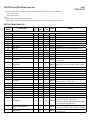 1
1
-
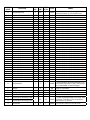 2
2
-
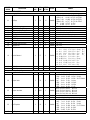 3
3
-
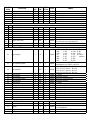 4
4
-
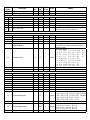 5
5
-
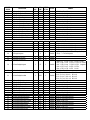 6
6
-
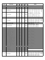 7
7
-
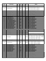 8
8
-
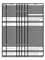 9
9
-
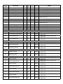 10
10
-
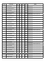 11
11
-
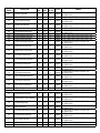 12
12
-
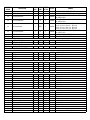 13
13
-
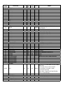 14
14
-
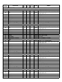 15
15
-
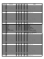 16
16
-
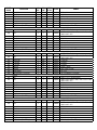 17
17
-
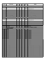 18
18
-
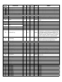 19
19
-
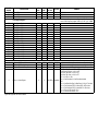 20
20
-
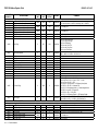 21
21
-
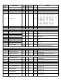 22
22
-
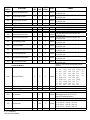 23
23
-
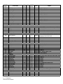 24
24
-
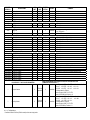 25
25
-
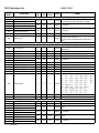 26
26
-
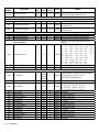 27
27
-
 28
28


red lion PAX2CHZ/VR Modbus Register Table User manual
- Type
- User manual
Ask a question and I''ll find the answer in the document
Finding information in a document is now easier with AI
Related papers
-
red lion PAX2C8H/8V Modbus Register Table User manual
-
-
red lion PXU21A20 Instructions Manual
-
-
-
-
red lion TCU Instruction User manual
-
-
-
Other documents
-
Omega CN63100 and CN63300 Series Owner's manual
-
Chromalox 4040 Operating instructions
-
-
Honeywell DCP200 User manual
-
-
-
Watlow Electric 160 Series User manual
-
-
-