
SERVICE MANUAL
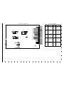
Contents
1. OUTLINE OF CIRCUIT DESCRIPTION ............................... 3
2. DISASSEMBLY ................................................................... 11
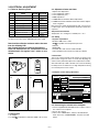
3. ELECTRICAL ADJUSTMENT ............................................. 21
4. USB STORAGE INFORMATION REGISTRATION ............ 27
5. TROUBLESHOOTING GUIDE............................................ 28
6. PARTS LIST........................................................................ 30
CIRCUIT DIAGRAMS & PRINTED WIRING BOARDS........... C1
CAUTION : Danger of explosion if battery is incorrectly replaced.
Replace only with the same or equivalent type recommended by the
manufacturer.
Discard used batteries according to the manufacturer’s instructions.
NOTE : 1. Parts order must contain model number, part number, and description.
2. Substitute parts may be supplied as the service parts.
3. N. S. P. : Not available as service parts.
Design and specification are subject to change without notice.
SG316/U, EX, GX, U2, EX2, GX2, U3, EX3, GX3 (R)
REFERENCE No. SM5310780
FILE NO.
Dual Camera
RoHS
•This product does not contain any hazardous substances prohibited by the RoHS
Directive.
WARNING
•You are requested to use RoHS compliant parts for maintenance or repair.
•You are requested to use lead-free solder.
(This product has been manufactured using lead-free solder. Be sure to follow the
warning given on page 2 when carrying out repair work.)
VPC-WH1W
(Product Code : 168 175 02)
(U.S.A.) (Canada) (Taiwan) (General)
VPC-WH1EXW
(Product Code : 168 175 03)
(Europe) (U.K.) (South America)
(China) (Australia) (Hong Kong)
(Russia) (Middle East) (Africa)
(General) (Korea) (Taiwan)
VPC-WH1GXW
(Product Code : 168 175 04)
(South America) (China)
(Australia) (Hong Kong)
(General) (Korea) (Taiwan)
VPC-WH1BL
(Product Code : 168 175 06)
(U.S.A.) (Canada) (Taiwan) (General)
VPC-WH1EXBL
(Product Code : 168 175 07)
(Europe) (U.K.) (South America)
(China) (Australia) (Hong Kong)
(Russia) (Middle East) (Africa)
(General) (Korea) (Taiwan)
VPC-WH1GXBL
(Product Code : 168 175 08)
(South America) (China)
(Australia) (Hong Kong)
(General) (Korea) (Taiwan)
VPC-WH1YL
(Product Code : 168 175 10)
(U.S.A.) (Canada) (Taiwan) (General)
VPC-WH1EXYL
(Product Code : 168 175 11)
(Europe) (U.K.) (South America)
(China) (Australia) (Hong Kong)
(Russia) (Middle East) (Africa)
(General) (Korea) (Taiwan)
VPC-WH1GXYL
(Product Code : 168 175 12)
(South America) (China)
(Australia) (Hong Kong)
(General) (Korea) (Taiwan)

– 2 –
WARNING
Do not use solder containing lead.
This product has been manufactured using lead-free solder in
order to help preserve the environment.
Because of this, be sure to use lead-free solder when carrying
out repair work, and never use solder containing lead.
Lead-free solder has a melting point that is 30 - 40°C (86 -
104°F) higher than solder containing lead, and moreover it does
not contain lead which attaches easily to other metals. As a
result, it does not melt as easily as solder containing lead, and
soldering will be more difficult even if the temperature of the
soldering iron is increased.
The extra difficulty in soldering means that soldering time will
increase and damage to the components or the circuit board
may easily occur.
Because of this, you should use a soldering iron and solder
that satisfy the following conditions when carrying out repair
work.
Soldering iron
Use a soldering iron which is 70 W or equivalent, and which
lets you adjust the tip temperature up to 450°C (842°F). It
should also have as good temperature recovery characteris-
tics as possible.
Set the temperature to 350°C (662°F) or less for chip compo-
nents, to 380°C (716°F) for lead wires and similar, and to 420°C
(788°F) when installing and removing shield plates.
The tip of the soldering iron should have a C-cut shape or a
driver shape so that it can contact the circuit board as flat or in
a line as much as possible.
Solder
Use solder with the metal content and composition ratio by
weight given in the table below. Do not use solders which do
not meet these conditions.
Lead-free solder is available for purchase as a service tool.
Use the following part number when ordering:
Part name: Lead-free solder with resin (0.5 mm dia., 500 g)
Part number: VJ8-0270
Metal content
Tin (Sn) Silver (Ag)
Copper (Cu)
Composition
ratio by weight
96.5 %
3.0 %
0.5 %
Note:
If replacing existing solder containing lead with lead-free sol-
der in the soldered parts of products that have been manufac-
tured up until now, remove all of the existing solder at those
parts before applying the lead-free solder.
The components designated by a symbol ( ! ) in this schematic diagram designates components whose value are of
special significance to product safety. Should any component designated by a symbol need to be replaced, use only the part
designated in the Parts List. Do not deviate from the resistance, wattage, and voltage ratings shown.
PRODUCT SAFETY NOTICE

– 3 –
1. OUTLINE OF CIRCUIT DESCRIPTION
1-1. CMOS CIRCUIT DESCRIPTION
1. IC Configuration
The CMOS peripheral circuit block basically consists of the
following ICs.
IC911 (MT9J001I12STCV)
CMOS imager
CDS, AGC, ADC built-in
H driver, V driver, serial communication circuit built-in
2. IC911 (CMOS)
[Structure]
The electric charges which are generated when each pixel is
optically converted are in turn converted into signal voltages
by the FD amplifier, and they are then transmitted by the built-
in H driver and V driver. The signals are sampled and ampli-
fied by the CDS and PGA circuits at the point they are output,
and then they are AD converted and output. The output uses
the 12 bit LVDS interface.
1/2.3-inch positive pixel array CMOS-type fixed imaging ele-
ment
Effective pixels 3856 (H) X 2764 (V)

– 4 –
1-2. CP1 and VF1 CIRCUIT DESCRIPTION
1. Circuit Description
1-1. Digital clamp
The optical black section of the extracts averaged values from
the subsequent data to make the black level of the output
data uniform for each line. The optical black section averaged
value for each line is taken as the sum of the value for the
previous line multiplied by the coefficient k and the value for
the current line multiplied by the coefficient k-1.
1-2. Signal processor
1. γ correction circuit
This circuit performs (gamma) correction in order to maintain
a linear relationship between the light input to the camera
and the light output from the picture screen.
2. Color generation circuit
This circuit converts the image sensor into RGB signals.
3. Matrix circuit
This circuit generates the Y signals, R-Y signals and B-Y sig-
nals from the RGB signals.
4. Horizontal and vertical aperture circuit
This circuit is used gemerate the aperture signal.
1-3. AE/AWB and AF computing circuit
The AE/AWB carries out computation based on a 64-segment
screen, and the AF carries out computations based on a 6-
segment screen.
1-4. SDRAM controller
This circuit outputs address, RAS, CAS and CS data for con-
trolling the SDRAM. It also refreshes the SDRAM.
1-5. Communication control
1. SDIO
This is the interface for the 8-bit microprocessor.
1-6. Digital encorder
It generates chroma signal from color difference signal.
2. Outline of Operation
When the shutter opens, the reset signals (ASIC and CPU)
and the serial signals (“take a picture” commands) from the
8-bit microprocessor are input and operation starts.
The picture data from CMOS passes through the A/D and
CDS, and is then input to the ASIC as digital data. The AF,
AE, AWB, shutter, and AGC value are computed from this
data, and three exposures are made to obtain the optimum
picture. The data which has already been stored in the SDRAM
is read by the CPU and color generation is carried out. Each
pixel is interpolated from the surrounding data as being ei-
ther R, G, and B primary color data to produce R, G and B
data. At this time, correction of the lens distortion which is a
characteristic of wide-angle lenses is carried out. After AWB
and γ processing are carried out, a matrix is generated and
aperture correction is carried out for the Y signal, and the
data is then compressed by JPEG and is then written to card
memory (SD card).
When the data is to be output to an external device, it is taken
data from the memory and output via the USB I/F. When played
back on the LCD and monitor, data is transferred from memery
to the SDRAM, and the image is then elongated so that it is
displayed over the SDRAM display area.
3. LCD Block
The LCD display circuit is located on the CP1 board and VF1
board, and consists of components such as a power circuit
and VCOM control circuit.
The signals from the ASIC are 8-bit digital signals, that is
input to the LCD directly. The 8-bit digital signals are con-
verted to RGB signals inside the LCD driver circuit. The LCD
is input signals from ASIC directly to the LCD, and function
such as image quality are controlled.
Because the LCD closes more as the difference in potential
between the VCOM (common polar voltage: AC) and the R,
G and B signals becomes greater, the display becomes darker;
if the difference in potential is smaller, the element opens and
the LCD become brighter.
In addition, the timing pulses for signals other than the video
signals are also input from the ASIC directory to the LCD.

– 5 –
5. Video Clip Recording and Playback
5-1. Recording
The signal from the camera block is input to IC101 (ASIC). The
data that is input to the ASIC is input to SDRAM, and converts
this data to encoded MPEG4 data, after which it is written in
sequence onto the SD card as streaming data. At this time,
the audio signals that are input to the built-in microphone are
converted into digital data by the audio CODEC IC of IC183,
and they are then input to ASIC. The audio data is then en-
coded (AAC), and then it is written in sequence onto the SD
card together as streaming data with the image signals de-
scribed above.
5-2. Playback
The data is read from the SD card, and the encoded data is
decoded into image data where it is displayed by the LCD or
on a TV monitor. At the same time, the audio data is also de-
coded, and is input to IC182 as digital data. D/A conversion is
carried out at IC182, and the sound is then output to the speaker
or to the LINE OUT terminal.
6. Audio CODEC Circuit (IC182)
The audio signals from the microphone are converted into 16-
bit digital data. AD conversion is carried out at a maximum
sampling frequency of 48 kHz.
During audio playback, the 16-bit digital data is converted into
analog signals and these drive headphone through the speaker
or line out system and headphone amplifier. DA conversion is
carried out at a maximum sampling frequency of 48 kHz.
4. Lens drive block
4-1. Focus drive
The 16-bit serial data signals (LENS_SDI) and (LENS_SCLK
and LENS_EN) which are output from the ASIC (IC101) are
used to drive (FOCUS A +, FOCUS A -, FOCUS B + and FO-
CUS B -) by the motor driver IC (IC951), and are then used to
microstep-drive the stepping motor for focusing operation. De-
tection of the standard focusing positions is carried out by
means of the photointerruptor (F_SENSE) inside the lens block.
4-2. Zoom drive
The 16-bit serial data signals (LENS_SDI) and (LENS_SCLK
and LENS_EN) which are output from the ASIC (IC101) are
used to drive (ZOOM A +, ZOOM A -, ZOOM B + and ZOOM B
-) by the motor driver IC (IC951), and are then used to
microstep-drive the stepping motor for zooming operation. De-
tection of the standard zooming positions is carried out by
means of the photointerruptor (F_SENSE) inside the lens block.
4-3. ND filter
The 16-bit serial data signals (LENS_SDI) and (LENS_SCLK
and LENS_EN) which are output from the ASIC (IC101) are
used to drive (ND + and ND –) by the motor driver IC (IC951),
and then the ND filter is inserted into and removed from the
beam path.
4-4. Iris drive
The drive method is a galvanometer type without braking coil.
The output from the Hall sensor inside the lens is amplified by
the Hall amplifier circuit inside the IC951 lens drive IC, and the
difference between the current and target aperture determined
by the resulting output and the exposure amout (16 bit serial
signal (LENS_SDI) and (LENS_SCLK and LENS_EN)) output
from the ASIC (IC101) is input to the servo amplifier circuit
(IC951) to keep the aperture automatically controlled (DRIVE+
and DRIVE -) to the target aperture.
4-5. Shutter drive
Reverse voltage is applied to the above aperture drive coil to
operate the shutter. When the shutter operates, the SHUTTER
+ signal that is output from the ASIC (IC101) becomes high
(input to SHUTTER of IC951) and the shutter operates.

– 6 –
1-3. PWA POWER CIRCUIT DESCRIPTION
1. Outline
This is the main power circuit, and is comprised of the follow-
ing blocks.
Switching controller (IC501)
Motor system power output (L5301)
Digital 3.25 V power output (L5002)
Digital 1.2 V power output (L5003)
Backlight power output (Q5007, L5007)
Digital and CMOS 1.8 V power output (IC504, L5006)
CMOS analog 2.8 V power output (IC503, L5005)
2. Switching Controller (IC501)
This is the basic circuit which is necessary for controlling the
power supply for a PWM-type switching regulator, and is pro-
vided with seven built-in channels, only CH1 (motor system),
CH2 (digital 3.25 V), CH3 (digital 1.2 V) and CH7 (backlight)
are used.
Each power supply output is received, and the PWM duty is
varied so that each one is maintained at the correct voltage
setting level.
Feedback for the backlight power (CH7) is provided to the
both ends voltage of registance so that regular current can
be controlled to be current that was setting.
2-1. Short-circuit protection circuit
If output is short-circuited for the length of time determined
by the condenser which is connected to Pin (A6) of IC501, all
output is turned off. To reset, momentarily set the control sig-
nal (P ON) to repeat control, or temporarily disconnect the
input power supply.
3. Motor System Power Output
BOOST 5 V is output. Feedback for the 5.0 V output is pro-
vided to the switching controller (Pin (B7) of IC501) so that
PWM control can be carried out.
4. Digital 3.25 V Power Output
VDD3 is output. Feedback for the VDD3 is provided to the
swiching controller (Pin (F3) of IC501) so that PWM control
can be carried out.
5. Digital 1.2 V Power Output
VDD 1.2 is output. Feedback for the 1.2 V is provided to the
switching controller (Pin (C3) of IC501) so that PWM control
to be carried out.
6. Backlight Power Supply output
Regular current is being transmitted to LED for LCD back-
light. Feedback for the both ends voltage of registance that is
being positioned to in series LED are provided to the switch-
ing controller (Pin (C4) of IC501) so that PWM control to be
carried out.
7. Digital and CMOS 1.8 V Power Output
VDD 1.8 is output. Feedback for the VDD 1.8 is provided to
the switching controller (Pin (3) of IC504) so that PWM con-
trol to be carried out.
8. CMOS Analog 2.8 V Power Output
VAA 2.8 is output. Feedback for the VAA 2.8 is provided to the
switching controller (Pin (3) of IC503) so that PWM control to
be carried out.

– 7 –
1-4. ST1 STROBE CIRCUIT DESCRIPTION
1. Charging Circuit
When UNREG power is supplied to the charge circuit and the
CHG signal from microprocessor becomes High (3.3 V), the
charging circuit starts operating and the main electorolytic
capacitor is charged with high-voltage direct current.
However, when the CHG signal is Low (0 V), the charging
circuit does not operate.
1-1. Charge switch
When the CHG signal switches to Hi, IC541 starts charging
operation.
1-2. Power supply filter
C5401 constitutes the power supply filter. They smooth out
ripples in the current which accompany the switching of the
oscillation transformer.
1-3. Oscillation circuit
This circuit generates an AC voltage (pulse) in order to in-
crease the UNREG power supply voltage when drops in cur-
rent occur. This circuit generates a drive pulse with a frequency
of approximately 200-300 kHz, and drive the oscillation trans-
former.
1-4. Oscillation transformer
The low-voltage alternating current which is generated by the
oscillation control circuit is converted to a high-voltage alter-
nating current by the oscillation transformer.
1-5. Rectifier circuit
The high-voltage alternating current which is generated at
the secondary side of T5401 is rectified to produce a high-
voltage direct current and is accumulated at electrolytic ca-
pacitor C5412.
1-6. Charge monitoring circuit
The functions programmed in the IC541 monitor oscillations
and estimate the charging voltage. If the voltage exceeds the
rated value, charging automatically stops. Then, the
ZCHG_DONE signal is changed to Lo output and a "charging
stopped" signal is sent to the microcomputer.
2. Light Emission Circuit
When FLCTL signal is input from the ASIC, the stroboscope
emits light.
2-1. Emission control circuit
When the FLCLT signal is input to the emission control cir-
cuit, Q5402 switches on and preparation is made to the light
emitting. Moreover, when a FLCLT signal becomes Lo, the
stroboscope stops emitting light.
2-2. Trigger circuit
The Q5402 is turned ON by the FLCLT signal and light emis-
sion preparation is preformed. Simultaneously, high voltage
pulses of several kV are emitted from the trigger coil and ap-
plied to the light emitter.
2-3. Light emitting element
When the high-voltage pulse form the trigger circuit is ap-
plied to the light emitting part, currnet flows to the light emit-
ting element and light is emitted.
Beware of electric shocks.

– 8 –
1-5. SYA CIRCUIT DESCRIPTION
1. Configuration and Functions
For the overall configuration of the SYA block, refer to the block diagram. The SYA block centers around a 8-bit microprocessor
(IC301), and controls camera system condition (mode).
The 8-bit microprocessor handles the following functions.
1. Operation key input, 2. Clock control and backup, 3. Power ON/OFF, 4. Storobe charge control
46
NOT USED
-
See next page →
Pin
Signal
1
2
3
4
5
6
7
8
9
11~14
15
16
17
18
19
20
24
26
27
28
29
33
34
35
36
37
38
39
42~44
47
40
45
ASIC_SCK
ZCARD
ZBACKUPCTL
CHG_CNT
HOT LINE
GREEN_LED
RED_LED
ST_CHG_ON
VDD2
SCAN IN4~1
ZUSB_DET
HDMI_HPD
ZCHG_DONE
TIMEOUT
BAT_UTX
BAT_URX
USB_ON
NOT USED
MRST
SW3.2ON
PON2
PLLEN
ERR
VSS3
VDD3
RDSEL
CLK (SFW)
DATA0 (SFW)
DC_IN
SCAN OUT2~0
ZOOM_SW_AD
ZAV_JACK
I/O
O
I
O
O
I
O
O
O
-
I
I
I
I
I
O
I
O
O
O
O
O
O
I
-
-
I
I
I
I
O
I
I
Outline
Serial clock output (CL required)
Card detection (SW3.2 V required)
Backup battery charge control
Camera charge permission
Hot line request from ASIC
Switch unit LED (green) (H= lighting)
Switch unit LED (red) (H= lighting)/ combine with UTX (CL required)
-
Keyscan input 4~1
USB power detection terminal (L= detection)
HDMI hot plug detection
Main condensor charge voltage detection
Charge done detection
Battery power detection IC UART sending
USB charge ON/OFF
(TGVD delete)
System reset (MRST)
SW 3.2 V power (L= 3.2 V)
Digital system power start-up signal
PLL enable signal
Charge error detection
-
-
Debugger select terminal
Debug CN
Debug CN
DC jack insertion detection (SW3.2 V required)
Keyscan output 2~0
Zoom key AD input
-
Cable detection
Battery power detection IC UART recieving
10
VSS2
-
-
21 SCAN_IN0
I
Keyscan input 0
22 PANEL_OPEN
I
Panel open detection (MR sensor)
23 KEY 2nd
I
S2 key input
Strobo charge control (H= charge)
25 SUB_REC
I
SUB REC key input
30 NOT USED
I (I2CSDATA delete)
31 P ON
O Digital system power start-up signal
32 NAND_RESET
O OneNAND reset
41 HINGE
I
Panel rotation detection

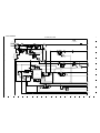
– 9 –
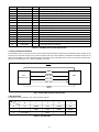
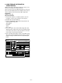
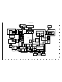
Fig. 5-1 Internal Bus Communication System
2. Internal Communication Bus
The SYA block carries out overall control of camera operation by detecting the input from the keyboard and the condition of the
camera circuits. The 8-bit microprocessor reads the signals from each sensor element as input data and outputs this data to the
camera circuits (ASIC) or to the LCD display device as operation mode setting data. Fig. 5-1 shows the internal communication
between the 8-bit microprocessor, ASIC and SPARC lite circuits.
Table 5-1. 8-bit Microprocessor Port Specification
8-bit
Microprocessor
ASIC
SREQ
ASIC_SDO
ASIC_SDI
ASIC_SCK
MRST
PLLEN
60
61
50
-
S1 key input
51
KEY_1st
I
-
56
NOT USED - -
VSS1
BATTERY
I UNREG voltage detection
58
59
ZSREQ
I
Serial communication request signal (CL required)
XOUT O 4M oscillation output
VDD1
-
-
49
BAT_OFF
I
Battery OFF detection signal input
52
ZBOOT_COMREQ
I/O
ZBOOT output
53
ZRESET
I
SBM reset input
54
XCIN
I
32 k oscillation input
55
XCOUT
O
32 k oscillation output
57
XIN I
4M oscillation input
48
BAT_TMP
I
Battery temperature detection
Serial data output (CL required)
Camera temperature detection
62
INT_TEMP I
63
ASIC_SDI O
64
ASIC_SDO
I
Serial data input (CL required)
3. Key Operaiton
For details of the key operation, refer to the instruction manual.
Table 5-2. Key Operation
0
0
123
SCAN
OUT
SCAN
IN
PLAY
RIGHT
UP
1
2
VREC
TEST -
-
LEFT
PW_TEST
MENU
DOWN
-
4
SET
-
POWER

– 10 –
ASIC,
memory
CMOS
8 bit CPU
Power voltage
Power OFF
Play back
LCD finder
3.3 V 1.0 V 1.8 V
2.8 V (A)
2.8 V (D), 1.8 V (D)
3.2 V
OFF
OFF
32KHz
OFF
OFF
32KHz
ON
ON
4 MHz
ON
OFF
4 MHz
Table 5-3. Camera Mode
Note) 4 MHz = Main clock operation, 32 kHz = Sub clock operation
4. Power Supply Control
The 8-bit microprocessor controls the power supply for the overall system.
The following is a description of how the power supply is turned on and off. When the battery is attached or DC IN input, a
regulated 3.2 V (power off: 2.4 V) voltage is normally input to the 8-bit microprocessor (IC301) by IC302, so that clock counting
and key scanning is carried out even when the power switch is turned off, so that the camera can start up again. When the battery
is removed and DC IN does not input, the 8-bit microprocessor operates in sleep mode using the backup battery. At this time, the
8-bit microprocessor only carries out clock counting, and waits in standby for the battery to be attached again or DC IN input.
When a switch is operated, the 8-bit microprocessor supplies power to the system as required.
The 8-bit microprocessor first set the P ON signal at pin (31) and the P ON2 signal at pin (29) to high, and then turns on the DC/
DC converter. After this, low signal is output from pin (27) so that the ASIC is set to the reset condition. After this these pins set
to high, and set to active condition. Once it is completed, the ASIC returns to the reset condition, all DC/DC converters are turned
off and the power supply to the whole system is halted.
Power switch ON - Auto power OFF
CAMERA

– 11 –
2. DISASSEMBLY
Note:
1. When disassembling and reassembling the main unit, the LCD and the battery cover, always be sure to use the air
leak tester (VJ8-0303), the SG316 air leak tester cradle (main body) (VJ8-0324) and the SG316 air leak tester
cradle (LCD) (VJ8-0325) to test for air leaks and to check that the waterproof mechanism is functioning normally.
Refer to the Instruction Manual provided with the air leak test tool for details on how to carry out the air leak test.
2. This camera uses waterproof packing. It is recommended that you replace the waterproof packing approximately
once every year. The waterproof packing is supplied in the COMPL, MENTE KIT-SV316 (P/No. 636 127 6870)
shown in the table below. These parts can also be supplied as single parts.
Summary of waterproof maintenance parts kit
Parts name: COMPL, MENTE KIT-SV316
Parts code: 636 127 6870
NO.
DESCRIPTION
1
2
4
SPACER PAD DC-SG316/J
5
1
NUMBER
6
1
GASKET CABINET-SG316/JP
1
GASKET LCD-SG316/JP
7
ASSY, COVER BATT SV-316/J 1
PAD DC-SG316/J
1
1ASSY, COVER TE SV-SG316
3 ASSY, GASKET SCREW-SV316
5
CABINET
LCD
COVER
BATTERY
PARTS NO.
6361278461
6361223362
6361223379
6361282772
6361223751
6361276658
6361276580
GASKET CABINET-SG316/JP
SECTION
List of waterproof maintenance parts kit
ASSY, GASKET SCREW-SV316
PAD DC-SG316/J
SPACER PAD
DC-SG316/J
ASSY, COVER TE
SV-SG316
GASKET LCD-SG316/JP
ASSY, COVER BATT
SV-316/J
SG316 air leak tester cradle (main body) (VJ8-0324)
SG316 air leak tester cradle (LCD) (VJ8-0325)

– 12 –
E
A
A
B
B
C
D
C
D
E
G
F
G
F
C
A
B
B
B
A
C
B
D
1
2
3
4
5
6
7
22-A
9
10
11
12
13
14
14-A
15
16
17
18
21
22
23
23
24
24
25
26
27
27
28
29
30
31
32
33
33
34
35
36
37
38
39
40
41
42
43
44
45
46
47
48
49
49
50
53
54
55
56
57
A
A
B
B
a
b
A
D
B
C
E
c
d
b
a
A
B
A
A
B
B
B
B
a
b
52
4-A
4-B
4-C
51
8
19
20
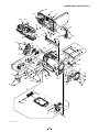
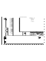
2-1. REMOVAL OF COMPL, CABI LEFT
When assembling,
tighten the screws order.
A → B → C
When assembling,
tighten the screws
order.
A → B
When assembling,
tighten the screws
order.
A → B → C → D
When assembling,
tighten the screws order.
a → b → c → d
When assembling,
tighten the screws
order.
A → B
When assembling,
tighten the screws order.
A → B → C → D → E
Must not touch the
Gore-Tex. (Because
of lose function of
waterproof.)
Remove from here
with tweezers.
Once remove the 4. Dec front,
change the new parts.
(4-A and 4-B) (nonreusable)
Once remove the 22-A.
Spacer cover air, change the
new parts. (nonreusable)

– 13 –
NOTE: Discharge a strobe capacitor
with the discharge jig (VJ8-0188) for
electric shock prevention.
1. Spacer bottom
2. Four screws 1.7 x 5
3. Ring lens
4. Dec front
4-A. Adhesive front A
4-B. Adhesive dec back 4
4-C. Spacer mic filter j
5. Four screws 1.4 x 4
6. Two screws 1.7 x 5
7. Dec grip
8. Spacer sw top
9. Four screws 1.7 x 5
10. Dec back
11. Holder button
12. Button shutter
13. Button movie
14. Button shutter in
14-A. Spacer pad back
15. Screw 1.7 x 5
16. Dec LED
17. Two screws 1.7 x 5
18. Dec top
19. Two screws 1.7 x 3
20. Dec DC
21. Four screws 1.7 x 4.5
22. Assy, dec joint
22-A. Spacer cover air
23. Two screws 1.7 x 7
24. Five screws 1.7 x 5
25. Compl, cabinet R LCD
26. FPC
27. Gasket screw
28. Screw 1.7 x 4
29. Holder right FL
30. Screw 1.7 x 3
31. Holder terminal batt
32. Remove the solder.
33. Four screws 1.7 x 5
34. FPC
35. Shaft cover DC
36. Spring cover DC
37. Compl, cover DC
38. Pad DC
39. Spacer pad DC
40. Two screws 1.7 x 3
41. Holder DC
When reassembling
The air leak test should
be carried out between
steps 22-A and 23.
At this time, the battery
cover should be closed
and locked.
After finishing the air leak
test, attach the new 22-A.
42. Two screws 1.7 x 4.5
43. Holder lock DC
44. Screw 1.7 x 4
45. Gasket screw
46. Screw 1.7 x 3
47. Earth cover batt
48. Shaft cover batt
49. Two screws 1.7 x 3
50. Shaft cover SD
51. Compl, dec left back sv
52. Assy, cover batt sv
53. Screw 1.7 x 3
54. Four screws 1.7 x 5
55. Stand
56. Four screws 1.7 x 3
57. Holder battery

– 14 –
14-A. Spacer pad back
35. Shaft cover DC
36. Spring cover DC
37. Compl, cover DC
8. Spacer sw top
22-A. Spacer cover air
4. Dec front
4-A. Adhesive front A
4-B. Adhesive dec back 4
4-C. Spacer mic filter j
4. Dec front
Do not distort the earth front.

– 15 –
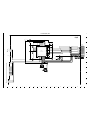
1. Attach from the lens side.
2. Pass the Top FPC
between DC and
the TB1 board.
3.
4.
5.
Back FPC
6.
7.
Must not touch
the Gore-Tex.
How to install the lens to the cabinet.

– 16 –
H
H
A
A
B
C
C
B
F
G
F
D
G
I
I
J
J
E
D
E
1
2
3
4
5
6
7
8
9
10
11
12
13
14
15
16
17
18
19
19
19
20
21
22
23
24
25
26
27
28
29
30
31
32
28
33
34
35
36
37
38
39
40
41
42
43
44
45
46
47
47
48
49
50
51
52
53
54
55
56
57
C
B
A
b
c
d
a
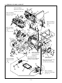
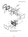
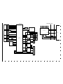
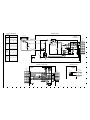
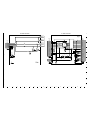
2-2. REMOVAL OF TB2 BOARD, TB1 BOARD, LENS, ST1 BOARD, CP1 BOARD AND TB3 BOARD
When assembling,
tighten the screws order.
a → b → c → d
When assembling,
tighten the screws order.
A → B → C

– 17 –
1. Remove the solder. (from TB2 board)
2. Remove the solder. (from speaker)
3. Holder TB2
4. Two screws 1.7 x 4
5. TB2 board
6. Speaker, 8
7. Shield tape LCD CP1
8. Spacer LCD CP1
9. FPC
10. Assy, FPC SUBREC
11. FPC
12. Shield tape socket 2
13. Screw 1.7 x 2.5
14. Screw 1.7 x 4
15. Two screws 1.7 x 4
16. Spacer earth TB1
17. TB1 board
18. Shield tape socket
19. Four screws 1.7 x 4
20. Holder TB1
21. Earth TB1
22. Two screws 1.7 x 4
23. Two screws 1.7 x 4
24. Holder lens chassis
25. Remove the lens part.
26. Holder lens
27. Connector
28. Three screws 1.4 x 3.5
29. Screw 1.7 x 2
30. Spacer heat CMOS
31. Mounting lens + assy, flexible pwb CA1
32. Spacer SUB CA
33. Holder lens
34. Spacer ST1
35. Two screws 1.7 x 7
36. Earth mic
37. Screw 1.7 x 3
38. Connector
39. ST1 board
40. Spacer mic 2
41. Holder dec flash
42. Cover triger
43. Remove the solder.
44. Assy, lamp
45. Remove the solder.
46. Spacer con ST1
47. Four screws 1.7 x 3
48. Flexible pwb CP1 & TB3
49. CP1 board
50. Spacer ST1
51. Heat sink rub ASIC
52. Two screws 1.7 x 3
53. Chassis bottom
54. Screw 1.7 x 2.5
55. TB3 board
56. Flexible pwb CP1 & TB3
57. Chassis right
5. TB2 board
30. Spacer heat CMOS
7. Shield tape LCD CP1
8. Spacer LCD CP1
16. Spacer earth TB1
44. Assy lamp dressing method43. Assy lamp soldering

– 18 –
A
A
B
B
1
2
3
4
5
6
7
8
9
10
11
12
13
14
15
16
18
19
20
21
23
25
26
27
28
29
30
31
32
33
24
B
B
A
A
17
A
B
22
3
4
5
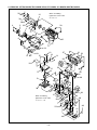
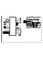
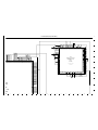
2-3. REMOVAL OF LCD AND VF1 BOARD
When assembling,
tighten the screws order.
A → B
VF1 board FPC dressing method
When exchanging the 5. Gasket screw,
do not take out the 4. Two screws
simultaneously.
Do not separate the joint
from the cabinet.

– 19 –
1. Gasket cabinet
1. Gasket cabinet
2. Shield tape cabinet
3. Spacer holder FPC
4. Two screws 1.7 x 4
5. Gasket screw
6. Two screws 1.7 x 4.5
7. Assy, dec LCD front
8. Two screws 1.7 x 4.5
9. Two screws 1.7 x 4.5
10. Cover LCD back
11. Gasket LCD
12. Shield tape VF1
13. Spacer VF1
14. FPC
15. FPC
16. Two screws 1.7 x 3
17. Compl, cover LCD front
18. Shield tape LCD FPC
19. Spacer LCD C
20. FPC
21. Spacer LCD B
22. Spacer LCD D
23. Spacer LCD A
24. LCD
25. Shield tape LCD
26. Three screws 1.7 x 2
27. VF1 board
28. Spacer pwb VF1
29. Holder LCD
30. Two screws 1.7 x 5
31. Dec cover terminal 2
32. Assy, cover te sv
33. Spacer knob terminal
When reassembling
The air leak test should
be carried out between
steps 7 and 8.
11. Gasket LCD
23. Spacer LCD A
21. Spacer LCD B
19. Spacer LCD C
22. Spacer LCD D

– 20 –
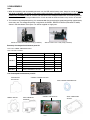
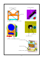
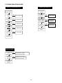
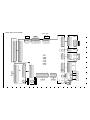
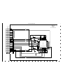
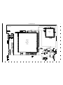
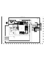
2-4. BOARD LOCATION
CP1 board
VF1 board
TB3 board
TB1 board
TB2 board
ST1 board
Page is loading ...
Page is loading ...
Page is loading ...
Page is loading ...
Page is loading ...
Page is loading ...
Page is loading ...
Page is loading ...
Page is loading ...
Page is loading ...
Page is loading ...
Page is loading ...
Page is loading ...
Page is loading ...
Page is loading ...
Page is loading ...
Page is loading ...
Page is loading ...
Page is loading ...
Page is loading ...
Page is loading ...
Page is loading ...
Page is loading ...
Page is loading ...
Page is loading ...
Page is loading ...
Page is loading ...
Page is loading ...
Page is loading ...
Page is loading ...
Page is loading ...
Page is loading ...
Page is loading ...
Page is loading ...
Page is loading ...
Page is loading ...
Page is loading ...
Page is loading ...
Page is loading ...
Page is loading ...
Page is loading ...
Page is loading ...
Page is loading ...
Page is loading ...
Page is loading ...
Page is loading ...
Page is loading ...
Page is loading ...
-
 1
1
-
 2
2
-
 3
3
-
 4
4
-
 5
5
-
 6
6
-
 7
7
-
 8
8
-
 9
9
-
 10
10
-
 11
11
-
 12
12
-
 13
13
-
 14
14
-
 15
15
-
 16
16
-
 17
17
-
 18
18
-
 19
19
-
 20
20
-
 21
21
-
 22
22
-
 23
23
-
 24
24
-
 25
25
-
 26
26
-
 27
27
-
 28
28
-
 29
29
-
 30
30
-
 31
31
-
 32
32
-
 33
33
-
 34
34
-
 35
35
-
 36
36
-
 37
37
-
 38
38
-
 39
39
-
 40
40
-
 41
41
-
 42
42
-
 43
43
-
 44
44
-
 45
45
-
 46
46
-
 47
47
-
 48
48
-
 49
49
-
 50
50
-
 51
51
-
 52
52
-
 53
53
-
 54
54
-
 55
55
-
 56
56
-
 57
57
-
 58
58
-
 59
59
-
 60
60
-
 61
61
-
 62
62
-
 63
63
-
 64
64
-
 65
65
-
 66
66
-
 67
67
-
 68
68


Sanyo VPC-WH1BL - Xacti Camcorder - 720p User manual
- Type
- User manual
- This manual is also suitable for
Ask a question and I''ll find the answer in the document
Finding information in a document is now easier with AI
Related papers
-
Sanyo VPC-TH1EXR User manual
-
Sanyo VPC-CG10P - Xacti Camcorder - 720p User manual
-
Sanyo VPC-CA8GXBK User manual
-
Sanyo VPC-CG11PXOR User manual
-
-
-
-
-
Sanyo Xacti VPC-HD1EX User manual
-
Other documents
-
FSR PWB-320XL-AC4 Installation guide
-
Siemens C10 User manual
-
Nikon Coolpix 4300 User manual
-
Hitachi KHWS1WUN User manual
-
DKS 1500 - 1506-081 Secondary Keypad User manual
-
KIA LAC-M5531EK User manual
-
Aiwa ADC-V107 User manual
-
Sharp 00ZFO3MKCUSME User manual
-
Contec VPC-700 Reference guide
-