Silicon Labs ETRX358x-LRS ZigBee® Modules Reference guide
- Type
- Reference guide

©2019 Silicon Labs
ETRX358x-LRS Product Manual
Telegesis™
TG-PM-0511-ETRX358x-LRS r8
ETRX358x-LRS and ETRX358xHR-LRS
Product Manual
Telegesis™ is a trademark of Silicon Laboratories Inc.
ETRX358x-LRS ZIGBEE
®
MODULES
PRODUCT MANUAL
Not Recommended for New Designs

ETRX358x-LRS and ETRX358xHR-LRS
©2019 Silicon Labs
- 2 -
ETRX358x-LRS Product Manual
Table of Contents
1 INTRODUCTION ................................................................................................................. 5
1.1 Hardware Description ....................................................................................................... 5
2 PRODUCT APPROVALS ........................................................................................................ 7
2.1 FCC Approvals ................................................................................................................. 7
2.1.1 FCC Labelling Requirements ............................................................................................ 8
2.2 IC (Industry Canada) Approvals ............................................................................................ 8
2.2.1 IC Labelling Requirements ............................................................................................... 9
2.3 European Certification .................................................................................................... 10
2.4 Declarations of Conformity ............................................................................................. 10
2.5 IEEE 802.15.4 ................................................................................................................ 10
2.6 The ZigBee Protocol ....................................................................................................... 11
3 MODULE PINOUT ................................................................................................................. 12
4 HARDWARE DESCRIPTION ............................................................................................ 14
4.1 Hardware Interface ......................................................................................................... 14
5 FIRMWARE DESCRIPTION .............................................................................................. 15
5.1 Token Settings ............................................................................................................... 16
5.2 Custom Firmware ........................................................................................................... 16
5.3 Boost Mode vs. Normal Mode............................................................................................. 16
6 A
BSOLUTE MAXIMUM RATINGS ................................................................................. 17
6.1 Environmental Characteristics ........................................................................................ 17
6.2 Recommended Operating Conditions ............................................................................. 17
7 DC ELECTRICAL CHARACTERISTICS ........................................................................... 18
8 DIGITAL I/O SPECIFICATIONS ........................................................................................ 20
9 A/D CONVERTER CHARACTERISTICS ........................................................................ 21
10 AC ELECTRICAL CHARACTERISTICS ......................................................................... 21
10.1 TX Power Characteristics ............................................................................................... 23
10.2 Power Settings for Regulatory Compliance ..................................................................... 24
10.3 Temperature behaviour ....................................................................................................... 25
11 PHYSICAL DIMENSIONS ................................................................................................. 26
12 RECOMMENDED REFLOW PROFILE ............................................................................. 27
13 PRODUCT LABEL DRAWING .......................................................................................... 28
14 RECOMMENDED FOOTPRINT ........................................................................................ 29
14.1 Recommended Placement
..............
............................................................................... 31
14.2 Example carrier board .................................................................................................... 33
15 RELIABILITY TESTS ............................................................................................................ 34
16 APPLICATION NOTES .................................................................................................. 34
Not Recommended for New Designs

ETRX358x-LRS and ETRX358xHR-LRS
©2019 Silicon Labs
- 3 -
ETRX358x-LRS Product Manual
16.1 Safety Precautions ......................................................................................................... 34
16.2 Design Engineering Notes .................................................................................................. 34
16.3 Storage Conditions ......................................................................................................... 35
17 PACKAGING .................................................................................................................... 36
17.1 Embossed Tape ............................................................................................................. 36
17.2 Component Orientation .................................................................................................. 37
17.3 Reel Dimensions ............................................................................................................ 37
17.4 Packaging ...................................................................................................................... 38
18 ORDERING INFORMATION ............................................................................................. 39
19 ROHS DECLARATION .......................................................................................................... 40
20 DATA SHEET STATUS .................................................................................................... 40
21 LIFE SUPPORT POLICY .................................................................................................. 40
22 RELATED DOCUMENTS .................................................................................................. 40
Not Recommended for New Designs

ETRX358x-LRS and ETRX358xHR-LRS
©2019 Silicon Labs
- 4 -
ETRX358x-LRS Product Manual
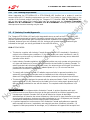
The Telegesis ETRX358x-LRS and ETRX358xHR-LRS
modules are low power 2.4GHz ZigBee modules with an added
frontend module (SiGe SE2432L) containing both PA and LNA
for highest possible link budget.
Based on the latest Ember EM358x family of single chip ZigBee
solutions the new long range modules are footprint compatible
with the entire Telegesis ETRX3 family, thus representing a
drop-in replacement for all applications where a high link
budget is required.
For custom application development the ETRX358x series
integrates with ease into Ember’s InSight development
environment.
Module Features
• Small form factor, SMT module 25mm x 19mm
• Same footprint and pin-out as ETRX357-LRS
• Side Castellations for easy soldering and inspection
• Two antenna options: Integrated chip antenna or U.FL
coaxial connector
• Based on 32-bit ARM® Cortex-M3
• Industry standard JTAG Programming and real time
network level debugging via the Ember Debug Port
• Up to 512kB of flash and 64kbytes of RAM
• Lowest Deep Sleep Current of sub 1µA with retained
RAM and GPIO and multiple sleep modes
• Ultra Wide supply voltage range (2.1 to 3.6V)
• Optional 32.768kHz watch crystal can be added
externally
• Can act as an End Device, Router or Coordinator
• 22 general-purpose I/O lines including analogue inputs
• Firmware upgrades via serial port or over the air
(password protected)
• Hardware supported encryption (AES-128)
• CE and FCC and IC compliance, IC and FCC modular
approval
• Operating temperature range: -40
°
C to +85
°
C
• Standard version without LNA and PA available in the
same form factor
Radio Features
• Based on the Silicon Labs EM358x family of single chip
ZigBee® SoCs
• 2.4GHz ISM Band
• 250kbit/s over the air data rate – NB: actual usable data
throughput with ZigBee is about 20kbps
• 15 channels (IEEE802.15.4 Channel 11 to 25)
• SiGe SE2432L integrated PA and LNA
• +20dBm output power (adjustable down to -41dBm)
• High sensitivity of -106dBm typ. @ 1% packet error rate
• RX Current: 33mA, TX Current: approx 140mA at
20dBm
Suggested Applications
• ZigBee Smart Energy applications
• Wireless Alarms and Security
• Home/Building Automation
• Wireless Sensor Networks
• M2M Industrial Controls
• Lighting and ventilation control
• Remote monitoring
• Environmental monitoring and control
Development Kit
• Enhancement kit available to upgrade existing
Telegesis and Ember development kits to be used with
the new ETRX358x family
• Custom software development available upon request.
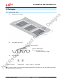
Image not shown actual size; enlarged to show detail.
Not Recommended for New Designs

ETRX358x-LRS and ETRX358xHR-LRS
©2019 Silicon Labs
- 5 -
ETRX358x-LRS Product Manual
This document describes the Telegesis ETRX358x-LRS and ETRX358xHR-LRS ZigBee long
range modules which have been designed to be easily integrated into another device and to
provide a fast, simple and low cost wireless mesh networking interface.
The Telegesis ETRX3 series modules are based on the Silicon Labs ZigBee compliant platform
consisting of the single chip family of EM358x SoCs combined with the ZigBee PRO compliant
EmberZNet meshing stack.
The ETRX358x-LRS and ETRX358xHR-LRS modules represent an ideal platform for custom
firmware development in conjunction with the Silicon Labs ZigBee development kits.
No RF experience or expertise is required to add this powerful wireless networking capability to
your products. The ETRX358x-LRS and ETRX358xHR-LRS offer fast integration opportunities
and the shortest possible time to market for your product.
The main building blocks of the ETRX358x-LRS and ETRX358xHR-LRS are the single chip
EM358x SoC from Silicon Labs, a SiGe SE2432L frontend module combining a Power Amplifier
with a Low Noise Amplifier, a 24MHz reference crystal and RF front-end circuitry optimized for best
RF performance. The modules are available with on-board antenna or alternatively a U.FL
connector for attaching external antennae. Modules with the U.FL connector are identified by the
“HR” suffix.
The integrated antenna is an Antenova Rufa, and details of the radiation pattern and further data
are available from the Antenova website [5].
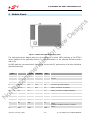
Module
Chip
Flash
RAM
Antenna
USB
ETRX3581-LRS
1
EM3581
256kB
32kB
Chip
No
ETRX3581HR-LRS
1
EM3581
256kB
32kB
External
No
ETRX3582-LRS
1
EM3582
256kB
32kB
Chip
Yes
ETRX3582HR-LRS
1
EM3582
256kB
32kB
External
Yes
ETRX3585-LRS
1
EM3585
512kB
32kB
Chip
No
ETRX3585HR-LRS
1
EM3585
512kB
32kB
External
No
ETRX3586-LRS
1
EM3586
512kB
32kB
Chip
Yes
ETRX3586HR-LRS
1
EM3586
512kB
32kB
External
Yes
ETRX3587-LRS
EM3587
512kB
64kB
Chip
No
ETRX3587HR-LRS
EM3587
512kB
64kB
External
No
ETRX3588-LRS
1
EM3588
512kB
64kB
Chip
Yes
ETRX3588HR
1
EM3588
512kB
64kB
External
Yes
Table 1: Memories
The LNA and RF power amplifier of the LRS devices improve the output power by 12dB and the
sensitivity by 5dB which will increase the range by approximately 700% relative to the standard
devices (where local regulations permit the use of the maximum output power).
1
MOQ and Lead Time applies. Only stocked modules are ETRX3587 and ETRX3587HR
1.1 Hardware Description
1 Introduction
Not Recommended for New Designs

ETRX358x-LRS and ETRX358xHR-LRS
©2019 Silicon Labs
- 6 -
ETRX358x-LRS Product Manual
The ETRX358x and ETRX358xHR are used for ZigBee (www.zigbee.org) applications. In case it is
desired to develop custom firmware, the Silicon Labs toolchain, consisting of Ember Desktop
together with a comprehensive integrated development environment (IDE), is required.
Not Recommended for New Designs

ETRX358x-LRS and ETRX358xHR-LRS
©2019 Silicon Labs
- 7 -
ETRX358x-LRS Product Manual
The ETRX358x-LRS and ETRX358xHR-LRS have been designed to meet all national regulations
for world-wide use. In particular the following certifications have been obtained:
The Telegesis ETRX358x-LRS family integrated Antenna as well as the ETRX358xHR-LRS family
including the antennas listed in and the power levels listed in section 10.2 have been tested to
comply with FCC CFR Part 15 (USA) The devices meet the requirements for modular transmitter
approval as detailed in the FCC public notice DA00.1407.transmitter.
FCC statement:
This device complies with Part 15 of the FCC rules. Operation is subject to the following
two conditions: (1) this device may not cause harmful interference, and (2) this device must
accept any interference received, including interference that may cause undesired
operation.
FCC ID: S4GEM358L
This module complies with the USA SAR requirements and is not intended to be operated within
20cm of the body. The following statement must be included as a CAUTION statement in manuals
for OEM products to alert users on FCC RF exposure compliance.
“WARNING: To satisfy FCC RF exposure requirements for mobile transmitting devices, a
separation distance of 20cm or more should be maintained between the antenna of this
device and persons during operation. To ensure compliance, operations at closer distances
than this are not recommended.”
Item
Part No.
Manufacturer
Type
Impedance
Gain
1
BT-Stubby
(straight)
EAD Ltd. [6] ¼ Wave
50Ω
0dBi
2
BT-Stubby
(right-angle)
EAD Ltd. [6] ¼ Wave
50Ω
0dBi
3
CJ-2400-6603
Chang Jia
½ Wave
50 Ω
2.0dBi
4
Rufa (on
board)
Antenova Chip
50Ω
2.1dBi
(peak)
Table 2. Approved Antennae
An end user deploying an ETRX358x-LRS or an ETRX358xHR-LRS module together with an
antenna as listed in Table 2 is not required to obtain a new authorization for the module – BUT this
does not preclude the possibility that some other form of authorization or testing may be required
for the end product depending upon local territorial regulations.
The FCC requires the user to be notified that any changes or modifications made to this device
that are not expressly approved by Telegesis (UK) Ltd. may void the user's authority to operate the
equipment. When using the ETRX358x-LRS with approved antennae, it is required to prevent end-
users from replacing them with non-approved ones.
2.1 FCC Approvals
2 Product Approvals
Not Recommended for New Designs

ETRX358x-LRS and ETRX358xHR-LRS
©2019 Silicon Labs
- 8 -
ETRX358x-LRS Product Manual
When integrating the ETRX358x-LRS or ETRX358xHR-LRS families into a product it must be
ensured that the FCC labelling requirements are met. This includes a clearly visible label on the
outside of the finished product specifying the Telegesis FCC identifier (FCC ID: S4GEM358L) as
well as the notice above. This exterior label can use wording such as “Contains Transmitter
Module FCC ID: S4GEM358L” or “Contains FCC ID: S4GEM358L” although any similar wording
that expresses the same meaning may be used.
The Telegesis ETRX358x-LRS family with integrated Antenna as well as the ETRX358xHR-LRS
family have been approved by Industry Canada to operate with the antenna types listed in Table 2
with the maximum permissible gain and required antenna impedance for each antenna type
indicated. Antenna types not included in this list, having a gain greater than the maximum gain
indicated for that type, are strictly prohibited for use with this device.
IC-ID: 8735A-EM358L
• This device complies with Industry Canada license-exempt RSS standard(s). Operation is
subject to the following two conditions: (1) this device may not cause interference, and (2)
this device must accept any interference, including interference that may cause undesired
operation of the device.
• U
nder Industry Canada regulations, this radio transmitter may only operate using an antenna
of a type and maximum (or lesser) gain approved for the transmitter by Industry Canada. To
reduce potential radio interference to other users, the antenna type and its gain should be so
chosen that the equivalent isotropically radiated power (e.i.r.p.) is not more than that
permitted for successful communication.
• To comply with Industry Canada RF radiation exposure limits for general population, the
antenna(s) used for this transmitter must be installed such that a minimum separation
distance of 20cm is maintained between the radiator (antenna) and all persons at all times
• This device has been designed to operate with the antennas listed in Table 2, and having a
maximum gain of 2.1 dBi. Antennas not included in this list or having a gain greater than 2.1
dBi are strictly prohibited for use with this device. The required antenna impedance is 50
ohms.
French Statements
• Conformément à la réglementation d'Industrie Canada, le présent émetteur radio peut
fonctionner avec une antenne d'un type et d'un gain maximal (ou inférieur) approuvé pour
l'émetteur par Industrie Canada. Dans le but de réduire les risques de brouillage
radioélectrique à l'intention des autres utilisateurs, il faut choisir le type d'antenne et son gain
de sorte que la puissance isotrope rayonnée équivalente (p.i.r.e.) ne dépasse pas l'intensité
nécessaire à l'établissement d'une communication satisfaisante.
• Le présent appareil est conforme aux CNR d'Industrie Canada applicables aux appareils
radio exempts de licence. L'exploitation est autorisée aux deux conditions suivantes : (1)
l'appareil ne doit pas produire de brouillage, et (2) l'utilisateur de l'appareil doit accepter tout
2.2 IC (Industry Canada) Approvals
2.1.1 FCC Labelling Requirements
Not Recommended for New Designs

ETRX358x-LRS and ETRX358xHR-LRS
©2019 Silicon Labs
- 9 -
ETRX358x-LRS Product Manual
brouillage radioélectrique subi, même si le brouillage est susceptible d'en compromettre le
fonctionnement.
OEM Responsibilities
The ETRX358x-LRS and ETRX358x-LRS families of module have been certified for integration into
products only by OEM integrators under the following conditions:
1. The antenna(s) must be installed such that a minimum separation distance of 0.75cm is
maintained between the radiator (antenna) and all persons at all times.
2. The transmitter module must not be co-located or operating in conjunction with any other
antenna or transmitter.
As long as the two conditions above are met, further transmitter testing will not be required.
However, the OEM integrator is still responsible for testing their end-product for any additional
compliance requirements required with this module installed (for example, digital device emissions,
PC peripheral requirements, etc.).
IMPORTANT NOTE: In the event that these conditions can not be met (for certain configurations
or co-location with another transmitter), then Industry Canada certification is no longer considered
valid and the IC Certification Number can not be used on the final product. In these circumstances,
the OEM integrator will be responsible for re-evaluating the end product (including the transmitter)
and obtaining a separate Industry Canada authorization.
The ETRX358x-LRS and ETRX358xHR-LRS family modules are labelled with its own IC Certification
Number. If the IC Certification Number is not visible when the module is installed inside another device,
then the outside of the device into which the module is installed must also display a label referring to the
enclosed module. In that case, the final end product must be labelled in a visible area with the following:
“Contains Transmitter Module IC: 8735A-EM358L”
or
“Contains IC: 8735A-EM358L”
The OEM of the ETRX358x-LRS and ETRX358xHR-LRS family modules must only use the approved
antenna(s) listed above, which have been certified with this module.
The OEM integrator has to be aware not to provide information to the end user regarding how to
install or remove this RF module or change RF related parameters in the user’s manual of the end
product.
2.2.1 IC Labelling Requirements
Not Recommended for New Designs

ETRX358x-LRS and ETRX358xHR-LRS
©2019 Silicon Labs
- 10 -
ETRX358x-LRS Product Manual
The ETRX358x and ETRX358xHR series modules with the power settings defined in section
10.2 are in conformity with the essential requirements and other relevant requirements of the Radio
Equipment Directive (RED) (2014/53/EU). These include
•
Radio:
EN 300 328 v2.1.1
•
EMC:
EN 301 489-17 v3.1.1
EN 301 489-
1 V2.1.1
• Safety: IEC 60950-1:2005, IEC 60950-1:2005/AMD1:2009,
IEC 60950-1:2005/AMD2:2013
Please note that every application using the modules will need to perform the radio EMC tests on the
end product, according to EN 301 489-17. It is ultimately the responsibility of the manufacturer to
ensure the compliance of the end product. The specific product assembly may have an impact to RF
radiated characteristics, and manufacturers should carefully consider RF radiated testing with the
end-product assembly. A formal DoC is available via www.silabs.com
The modules are in conformity with the essential requirements and other relevant requirements of
the Radio Equipment Directive (RED) with the antennae listed in Table 2.
Telegesis (UK) Ltd has issued Declarations of Conformity for all ETRX3 series ZigBee RF
Modules, which cover Radio Emissions and Safety. These documents will be available from our
website or on request
IEEE 802.15.4 is a standard for low data rate, wireless networks (raw bit-rate within a radio packet
of 250kbps @2.4GHz) which focuses on low cost, low duty cycle, long primary battery life
applications as well as mains-powered applications. It is the basis for the open ZigBee Protocol.
2.5 IEEE 802.15.4
2.4 Declarations of Conformity
2.3 European Certification
Not Recommended for New Designs

ETRX358x-LRS and ETRX358xHR-LRS
©2019 Silicon Labs
- 11 -
ETRX358x-LRS Product Manual
The ZigBee Protocol is a set of standards for wireless connectivity for use between any devices
over short to medium distances. The specification was originally ratified in December 2004, paving
the way for companies to start making low-power networks a reality.
ZigBee uses an IEEE 802.15.4 radio specification running on the 2.4GHz band, plus three
additional layers for networking, security and applications. What makes the specification unique is
its use of a mesh network architecture which, in bucket chain style, passes data from one node to
the next until it lands at its destination. The network is self-healing and adapts its routing as link
quality changes or nodes move. Furthermore, nodes can be defined as End Devices which do not
act as routers, but can therefore be put into a low-power sleep state.
The enhanced version of the ZigBee standard (or ZigBee 2006) was released in December 2006,
adding new features and improvements to the only global wireless communication standard
enabling the development of easily deployable low-cost, low-power, monitoring and control
products for homes, commercial buildings and industrial plant monitoring. In 2007 the ZigBee
Alliance introduced the PRO feature-set which offers advantages over earlier feature-sets,
including
• Tr
uly self-healing mesh networking
• Messages can now travel up to 30 hops
• Source-Routing for improved point to multipoint message transmission
• Improved security including Trust-Centre link keys
• New message types and options
2.6 The ZigBee Protocol
Not Recommended for New Designs

ETRX358x-LRS and ETRX358xHR-LRS
©2019 Silicon Labs
- 12 -
ETRX358x-LRS Product Manual
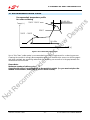
Figure 1. ETRX3 series Module Pinout (top view)
The table below gives details about the pin assignment for direct SMD soldering of the ETRX3
series modules to the application board. For more information on the alternate functions please
refer to [2].
All GND pads are connected within the module, but for best RF performance all of them should be
grounded externally.
ETRX358x
pad
Name
Defaul
t
Use
Alternate
function
EM35x
pin
Alternate functions
1
GND
GND
GND
2 PC5 {1} I/O TX_ACTIVE 11
TX_ACTIVE. PC5 of the EM35x is used to control
the FEM
3
PC6
I/O
13
OSC32B, nTX_ACTIVE
4
PC7
I/O
14
OSC32A, OSC32_EXT
5
PA7 {4}
I/O
18
TIM1C4
6
PB3 {2}
I/O
CTS
19
SC1nCTS, SC1SCLK, TIM2C3
7
nReset {5}
nReset
12
8
PB4 {2}
I/O
RTS
20
TIM2C4, SC1nRTS, SC1nSSEL
9
PA0
I/O
21
TIM2C1, SC2MOSI,USBDM{6}
10
PA1
I/O
22
TIM2C3, SC2SDA, SC2MISO,USBDP{6}
11
PA2
I/O
24
TIM2C4, SC2SCL, SC2SCLK
12
PA3
I/O
25
SC2nSSEL, TIM2C2
13
GND
GND
GND
14
PA4
I/O
26
ADC4, PTI_EN, TRACEDATA2
15
PA5 {3}
I/O
27
ADC5, PTI_DATA, nBOOTMODE, TRACEDATA3
16
PA6 {4}
I/O
29
TIM1C3
17 PB1 TXD
30
SC1MISO, SC1MOSI, SC1SDA, SC1TXD,
TIM2C1
18 PB2 RXD
31
SC1MISO, SC1MOSI, SC1SCL, SC1RXD,
TIM2C2
19
GND
GND
GND
3 Module Pinout
Not Recommended for New Designs

©2019 Silicon Labs
- 13 -
ETRX358x-LRS Product Manual
ETRX358x-LRS and ETRX358xHR-LRS
ETRX358x
pad
Name
Defaul
t
Use
Alternate
function
EM35x
pin
Alternate functions
20
GND
GND
GND
21
JTCK
JTCK
32
SWCLK
22
PC2
I/O
33
JTDO, SWO, TRACEDATA0
23
PC3
I/O
34
JTDI, TRACECLK
24
PC4
I/O
35
JTMS, SWDIO
25
N/C{1}
N/C
36
PB0 of the EM35x is used to control the FEM
26
PC1
I/O
ADC3
38
ADC3, TRACEDATA3
27
PC0 {4}
I/O
40
JRST, IRQD, TRACEDATA1
28
PB7 {4}
I/O
ADC2
41
ADC2, IRQC, TIM1C2
29
PB6 {4}
I/O
ADC1
42
ADC1, IRQB, TIM1C1
30
PB5
I/O
ADC0
43
ADC0, TIM2CLK, TIM1MSK
31
GND
GND
GND
32
Vcc
Vcc
Vcc
33
GND
GND
GND
Notes:
Table 3. Pin Information
{1} When the alternate GPIO function is selected, TX_ACTIVE becomes an output that indicates that
the EM35x radio transceiver is in transmit mode. PC5 must not be used in this mode as it is needed
internally as TX_ACTIVE to control the external RF front end and power amplifier. PB0 is not
available to the user.
{2} The serial UART connections TXD, RXD, CTS and RTS are PB1, PB2, PB3 and PB4 respectively.
The device sends its data on TXD and receives on RXD.
{3} If PA5 is driven low at power-up or reset the module will boot up in the bootloader
{4} PA6, PA7, PB6, PB7 and PC0 can drive high current (see section 8)
{5} nRESET is level-sensitive, not edge-sensitive. The module is held in the reset state while nRESET
is low. This signal has a 30kΩ Pull-Up.
{6} ETRX3588, ETRX3586, ETRX3582 and ETRX3588HR, ETRX3586HR, ETRX3582HR variants only
Important Note: The ETRX358x series and the ETRX358x-LRS series of modules are footprint
compatible, but on the ETRX358x-LRS series pins PB0 and PC5 of the EM358x are used
internally to control the front-end module and are not available to the user. PC5 is still available on
Pad2, but it is configured as TX_ACTIVE signal and cannot be used as a general purpose GPIO.
See also the table “Module pads and functions” in the ETRX357 Development Kit Product Manual.
Refer to the Silicon Labs EM358x manual for details of the alternate functions and pin names.
Not Recommended for New Designs

ETRX358x-LRS and ETRX358xHR-LRS
©2019 Silicon Labs
- 14 -
ETRX358x-LRS Product Manual
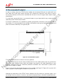
integrated
antenna
Vreg
Vcc
1,8Vdc
LDO
1V8
LDO
1V25
EM358x
I/O
A/D
UART
USB*
I / O
RESET
5 JTAG
RESET
programming
24MHz
*not available on all Types
Figure 2. Hardware Diagram
The ETRX358x-LRS and ETRX358x-LRS are based on the Silicon Labs EM358x family of ZigBee
SoCs in addition to a frontend module containing a PA, LNA and RF switch in addition to the RF-
frontend circuitry. The EM358x family of ZigBee SoCs are fully integrated 2.4GHz ZigBee
transceivers with a 32-bit ARM
®
Cortex M3
TM
microprocessor, flash and RAM memory, and
peripherals.
The industry standard serial wire and JTAG programming and debugging interfaces together with
the standard ARM system debug components help to streamline any custom software
development.
In addition to this a number of MAC functions are also implemented in hardware to help maintain
the strict timing requirements imposed by the ZigBee and IEEE802.15.4 standards.
The new advanced power management features allow faster wakeup from sleep and new power-
down modes allow this 3
rd
generation module to offer a longer battery life than any 2
nd
generation
modules on the market.
The EM358x has fully integrated voltage regulators for both required 1.8V and 1.25V supply
voltages. The voltages are monitored (brown-out detection) and the built in power-on-reset circuit
eliminates the need for any external monitoring circuitry. A 32.768kHz watch crystal can be
connected externally to pads 3 and 4 in case more accurate timing is required.
All GPIO pins of the EM358x chips are accessible on the module’s pads. Whether signals are
used as general purpose I/Os, or assigned to a peripheral function like ADC is set by the firmware.
When developing custom firmware please refer to the EM358x datasheet [2].
4.1 Hardware Interface
4 Hardware Description
FEM
Match
Match
rf
terminal
selection,
filtering and
matching
circuitry
U.FL socket
Not Recommended for New Designs

©2019 Silicon Labs
- 15 -
ETRX358x-LRS Product Manual
ETRX358x-LRS and ETRX358xHR-LRS
By default, the modules will be pre-loaded with a standalone bootloader which supports over-the-
air bootloading as well as serial bootloading of new firmware.
In order to enter the standalone bootloader using a hardware trigger pull PA5 to ground and
power-cycle or reset the module. To avoid entering the standalone bootloader unintentionally
make sure not to pull this pin down during boot-up unless the resistance to ground is >10kΩ. (A
pull-up is not required).
Each module comes with a unique 64-bit 802.15.4 identifier which is stored in non-volatile memory.
A router is typically a mains powered device whilst a sleepy end device (SED) can be battery
powered.
The module is also able to act as a coordinator and Trust Centre through external host control.
5 Firmware Description
Not Recommended for New Designs

©2019 Silicon Labs
- 16 -
ETRX358x-LRS Product Manual
ETRX358x-LRS and ETRX358xHR-LRS
The ETRX358x-LRS Series Modules’ manufacturing tokens will be pre-programmed with the
settings shown in the table below.
Token
Description
TG Default
MFG_CIB_OBS
Option Bytes
<not written>
MFG_CUSTOM_VERSION
Optional Version Number
<not written>
MFG_CUSTOM_EUI_64
Custom EUI
<not written>
MFG_STRING
Device Specific String
TELEGESIS
MFG_BOARD_NAME
Hardware Identifier
<Order Code>
MFG_MANUF_ID
Manufacturer ID
0x1010
MFG_PHY_CONFIG
Default Power Settings
0xFFFD
MFG_BOOTLOAD_AES_KEY
Bootloader Key
<not written>
MFG_EZSP_STORAGE
EZSP related
<not written>
MFG_CBKE_DATA
SE Security
<not written>
MFG_INSTALLATION_CODE
SE Installation
<not written>
MFG_OSC24M_BIAS_TRIM
Crystal Bias
<not written>
MFG_SYNTH_FREQ_OFFSET
Frequency offset
<not written>
MFG_OSC24M_SETTLE_DELAY
Crystal Stabilizing Time
<not written>
MFG_SECURITY_CONFIG
Security Settings
<not written>
MFG_CCA_THRESHOLD
CCA Threshold
0xFEBF
MFG_SECURE_BOOTLOADER_KEY
Secure Bootloader Key
<not written>
Table 4. Manufacturing tokens
The ETRX358x-LRS series of modules is an ideal platform for developing custom firmware. In
order to develop custom firmware the Silicon Labs Ember toolchain is required.
When writing firmware for the ETRX358x-LRS it is important to ensure that pins PB0 and PC5 are
correctly configured in order that the RF front-end module can operate correctly. An application
note “Writing customised firmware for the ETRX35x-LRS” can be downloaded from the Telegesis
website.
The Ember EM358x chips support a “boost mode” power setting next to the “normal mode” power
setting. The “boost mode” setting increases the sensitivity and output power of the radio
transceiver, however with the LRS variants enabling boost mode has no positive effect on neither
the output power nor the sensitivity and therefore it is recommended to not use boost mode on this
platform.
Section 10.2 lists the requirements for the maximum power settings for use of the LRS family in
different countries.
5.3 Boost Mode vs. Normal Mode
5.2 Custom Firmware
5.1 Token Settings
Not Recommended for New Designs

©2019 Silicon Labs
- 17 -
ETRX358x-LRS Product Manual
ETRX358x-LRS and ETRX358xHR-LRS
No.
Item
Symbol
Absolute Maximum Ratings
Unit
1
Supply voltage
V
CC
-0.3 to +3.6
Vdc
2
Voltage on any Pad
V
in
-0.3 to V
CC
+0.3
Vdc
3
Voltage on any Pad pin (PA4, PA5, PB5,
PB6, PB7, PC1), when used as an input
to the general purpose ADC with the
low voltage range selected
V
in
-0.3 to +2.0
Vdc
4
Module storage temperature range
T
stg
-40 to +105
°C
5
Reel storage temperature range
T
strgreel
0 to 75
°C
6
Operating temperature range
T
op
-40 to +85
°C
7
Input RF level
P
max
+6
dBm
8
Reflow temperature
T
Death
Please refer to chapter 12
°C
Table 5: Absolute Maximum Ratings
The absolute maximum ratings given above should under no circumstances be violated.
Exceeding one or more of the limiting values may cause permanent damage to the device.
Caution! ESD sensitive device. Precautions should be used when handling the device
in order to prevent permanent damage.
No.
Item
Symbol
Absolute Maximum Ratings
Unit
1
ESD on any pad according to
Human Body Model (HBM) circuit
description
V
THHBM
±2
kV
2
ESD on non-RF pads according to
Charged Device Model (CDM) circuit
description
V
THCDM
±400
V
3
ESD on RF terminal (HBM)
V
THCDM
1000
V
4
Moisture Sensitivity Level
MSL
MSL3, per J-STD-033
Table 6: Absolute Maximum Ratings
Table 7. Recommended Operating Conditions
No.
Item
Conditon/
Remark
Symbol
Value Unit
Min
Typ
Max
1
Supply voltage
V
CC
2.1
3.6
Vdc
2
RF Input Frequency
f
C
2405
2480
MHz
3
RF Input Power
p
IN
0
dBm
4
Operating temperature range
T
op
-40
+85 °C
6.2 Recommended Operating Conditions
6.1 Environmental Characteristics
6 Absolute Maximum Ratings
Not Recommended for New Designs

©2019 Silicon Labs
- 18 -
ETRX358x-LRS Product Manual
V
CC
= 3.0V, T
AMB
= 25°C, NORMAL MODE (non-Boost) unless otherwise stated
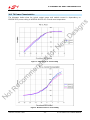
No. Item
Condition /
Remark
Symbol Value Unit
Min
Typ
Max
1
Module supply voltage
V
CC
2.1
3.6
Vdc
Deep Sleep Current
2
Quiescent current,
internal RC oscillator
disabled,
4kB RAM retained I
SLEEP
1.0 µA
3
Quiescent current,
internal RC oscillator
enabled
4kB RAM retained I
SLEEP
1.25 µA
4
Quiescent current,
including
32.768kHz oscillator
4kB RAM retained I
SLEEP
1.6 µA
5
Quiescent current including
internal RC oscillator and
32.768kHz oscillator
4kB RAM retained I
SLEEP
1.9 µA
6
Additional current per 4kB
block of RAM retained
I
RAMSLEEP
0,067 µA
Reset Current
7
Quiescent current nReset
asserted
I
RESET
2 3 mA
Processor and Peripheral Currents
8
ARM
®
Cortex
TM
M3, RAM
and flash memory
25°C, 12MHz Core
clock
I
MCU
7.5 mA
9
ARM
®
Cortex
TM
M3, RAM
and flash memory
25°C, 24MHz Core
clock
I
MCU
8.5 mA
10
ARM
®
Cortex
TM
M3, RAM
and flash memory sleep
current
25°C, 12MHz Core
clock
I
MCU
4.0 mA
11
ARM
®
Cortex
TM
M3, RAM
and flash memory sleep
current
25°C, 6MHz Core
clock
I
MCU
2.5 mA
12 Serial controller current
Per serial controller
at max. clock rate
I
SC
0.2 mA
13
General purpose timer
current
Per timer at max.
clock rate
I
TIM
0.25 mA
14
General purpose ADC
current
Max. Sample rate,
DMA
I
ADC
1.1 mA
15
USB Active Current
I
USB
1
mA
16
USB Suspend Mode
Current
I
USBSUSP
2.5 mA
RX Current
17
LNA,Radio receiver MAC
and Baseband
ARM
®
Cortex
TM
M3
sleeping.
I
RX
26.5 mA
18
Receive current
consumption
Total, 12MHz clock
speed
I
RX
30 mA
19
Receive current
consumption
Total, 24MHz clock
speed
I
RX
31.5 mA
7 DC Electrical Characteristics
Not Recommended for New Designs

©2019 Silicon Labs
- 19 -
ETRX358x-LRS Product Manual
TX Current
20
Transmit current
consumption
at +20dBm module
output power
I
TXVCC
140 mA
21
Transmit Current
consumption
at min module
output power
I
TXVCC
52 mA
Sleep Modes & Peripheral Current
22
MCU, RAM and flash, FEM,
radio off
12MHz clock speed I
MCU
7 mA
23
MCU, RAM and flash, FEM,
radio off
24MHz clock speed I
MCU
8 mA
24
Serial Controller
Max data rate
I
SC
0.2
mA
25
Timer
Max clock rate
I
TMR
0.25
mA
26
ADC
Max sample rate
I
ADC
1.1
mA
Not Recommended for New Designs

©2019 Silicon Labs
- 20 -
ETRX358x-LRS Product Manual
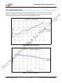
The digital I/Os of the ETRX358x-LRS module have the ratings shown below.
V
CC
= 3.0V, T
AMB
= 25°C, NORMAL MODE unless otherwise stated
No. Item
Condition /
Remark
Symbol Value Unit
Min
Typ
Max
1
Low Schmitt switching
threshold
Schmitt input
threshold going from
high to low
V
SWIL
0.42 x V
CC
0.5 x V
CC
Vdc
2
High Schmitt switching
threshold
Schmitt input
threshold going from
low to high
V
SWIH
0.62 x V
CC
0.8 x V
CC
MHz
3
Input current for logic 0
I
IL
-0.5
µA
4
Input current for logic 1
I
IH
0.5
µA
5
Input Pull-up resistor value
R
IPU
24
29
34
kΩ
6
Input Pull-down resistor
value
R
IPD
24 29 34 kΩ
7 Output voltage for logic 0
I
OL
= 4mA (8mA) for
standard (high
current) pads
V
OL
0 0.18 x V
CC
V
8 Output voltage for logic 1
I
OH
= 4mA (8mA)for
standard (high
current) pads
V
OH
0.82 x V
CC
V
CC
V
9
Output Source Current
Standard current pad
I
OHS
4
mA
10
Output Sink current
Standard current pad
I
OLS
4
mA
11
Output Source Current
High current pad (1)
I
OHH
8
mA
12
Output Sink current
High current pad (1)
I
OLH
8
mA
13
Total output current
I
OH
+ I
OL
40
mA
Table 9. Digital I/O Specifications
No. Item
Condition /
Remark
Symbol Value Unit
Min
Typ
Max
1
Low Schmitt switching
threshold
Schmitt input
threshold going from
high to low
V
SWIL
0.42 x V
CC
0.5 x V
CC
Vdc
2
High Schmitt switching
threshold
Schmitt input
threshold going from
low to high
V
SWIH
0.62 x V
CC
0.68 x V
CC
Vdc
3
Input current for logic 0
I
IL
-0.5
µA
4
Input current for logic 1
I
IH
0.5
µA
5
Input Pull-up resistor value
Chip not reset
R
IPU
24
29
34
kΩ
6
Input Pull-up resistor value
Chip reset
R
IPURESET
12
14.5
17
kΩ
Notes
Table 10. nReset Pin Specifications
1) High current pads are PA6, PA7, PB6, PB7, PC0
8 Digital I/O Specifications
Not Recommended for New Designs
Page is loading ...
Page is loading ...
Page is loading ...
Page is loading ...
Page is loading ...
Page is loading ...
Page is loading ...
Page is loading ...
Page is loading ...
Page is loading ...
Page is loading ...
Page is loading ...
Page is loading ...
Page is loading ...
Page is loading ...
Page is loading ...
Page is loading ...
Page is loading ...
Page is loading ...
Page is loading ...
Page is loading ...
-
 1
1
-
 2
2
-
 3
3
-
 4
4
-
 5
5
-
 6
6
-
 7
7
-
 8
8
-
 9
9
-
 10
10
-
 11
11
-
 12
12
-
 13
13
-
 14
14
-
 15
15
-
 16
16
-
 17
17
-
 18
18
-
 19
19
-
 20
20
-
 21
21
-
 22
22
-
 23
23
-
 24
24
-
 25
25
-
 26
26
-
 27
27
-
 28
28
-
 29
29
-
 30
30
-
 31
31
-
 32
32
-
 33
33
-
 34
34
-
 35
35
-
 36
36
-
 37
37
-
 38
38
-
 39
39
-
 40
40
-
 41
41


Silicon Labs ETRX358x-LRS ZigBee® Modules Reference guide
- Type
- Reference guide
Ask a question and I''ll find the answer in the document
Finding information in a document is now easier with AI
Related papers
-
Silicon Labs ETRX358x ZigBee® Modules Reference guide
-
Silicon Laboratories ETRX357DVK – Telegesis Development Kit for ZigBee® Technology User manual
-
-
-
-
-
-
-
-
Other documents
-
 OSRAM SYLVANIA 73742 User manual
-
 Telegesis ETRX358xHR-LRS User manual
-
Commax CRM-1356BM User manual
-
 LumenRadio CRMX 200-1901 Manuallines
-
Furrion WF8023 Wireless Module User manual
-
Continental ARS5A User guide
-
 logika WL-ZTPCNPB-I020-01 User manual
-
 Telegesis ZigBee ETRX3USB+8M User manual
-
RTI ZB-Pro Operating instructions
-
Uconnect ZA-L2 User manual


