Page is loading ...

AXM0F343 SDK Getting Started Guide
©
Semiconductor
Component
Industries,
LLC,
2021
1
April, 2021 – Rev. 1.3

AXM0F343 SDK Getting Started Guide
http://onsemi.com
2
Contents
Introduction............................................................................................................................ 3
Hardware Setup ..................................................................................................................... 3
System Overview ...................................................................................................................................................................... 3
Headers Configuration .............................................................................................................................................................. 4
AXM0F343 IC Pinout and DVK connections ............................................................................................................................ 5
IDE and SDK Setup ............................................................................................................... 7
Prerequisites ............................................................................................................................................................................. 7
IDE Installation ......................................................................................................................................................................... 7
AXM0F343 SDK Installation .................................................................................................................................................... 7
Working with Example Applications .................................................................................. 10
Importing and Building Applications ....................................................................................................................................... 10
Advanced Configuration and Debugging ................................................................................................................................. 12

AXM0F343 SDK Getting Started Guide
http://onsemi.com
3
Introduction
The AXM0F343 combines the industry-leading AX5043 sub-GHz transceiver with a low-power Arm® Cortex-M0+
processor useful for various wireless applications. The AXM0F343 SDK includes the necessary firmware, software,
example projects,
documentation, and development tools to begin building end applications on the platform. This SDK
is built on the Eclipse-based
ON Semiconductor Integrated Development Environment (IDE), which is available as a
free download from the AXM0F343 product page.
All example applications, device drivers, and application configuration files are delivered in a CMSIS pack format. This
enables
a modular approach that simplifies the set-up, compilation, and programming of reference example code on the
AXM0F343 Development Kit boards. The following sections will describe the process of installing and using the SDK.
Please refer to the readme files included with the example projects for additional descriptions of the applications and
their configuration and use.
Hardware Setup
System Overview
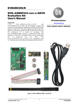
The AXM0F343-X-X-1-GEVB are a series of evaluation boards intended for use in conjunction with the AXM0F343-
SDK. The first -X represents the memory
configuration, while the second represents the frequency.
For example, AXM0F343-256-915-1-GEVB has the IC variant with 256 kB of FLASH and the RF matching network
is tuned for 915 MHz operation.
The board can be powered via USB, CR2032 battery, or an external 3.3V DC source via the Arduino-compatible header.
Both SWD and Serial interfaces are provided via the J-Link On-Board. The AXM0F343 can be configured to output the
RF signal via a differential load network, which supports both TX and RX, or a power-efficient single-ended network,
which only supports TX. The block diagram of the system is shown below:
Figure 1 - AXM0F343-x-x-1-GEVB block diagram
NOTE: By default, the boards do not have the single-ended SMA installed. This is because the example software is
designed to use the differential interface. Software configuration must be done to switch between single-ended and
differential output networks.

AXM0F343 SDK Getting Started Guide
http://onsemi.com
4
Evaluation Kit Content
The AXM0F343-X-X-1-GEVK evaluation kit includes all what is needed to start testing and developing RF
applications:
2x AXM0F343-X-X-1-GEVB boards pre-loaded with AX-Radio-TX and AX-Radio-RX examples;
2x Micro-USB cables;
2x whip antennas;
Components bag with PCB mounting feet, extra headers, and an SMA connector that can be mounted when
needed as shown in the figure below.
Figure 2: AXM0F343-x-x-1-GEVK content.
Headers Configuration
Figure 3 highlights several power headers available on the AXM0F343-X-X-1-GEVB that allow to connect/disconnect
power domains and to monitor the currents:
Supply: the yellow “Supply” arrow shows the main power selector. With this selector the power source can be
toggled between battery operation (BATT) and USB or external voltage (USB/VIN).
J10: this 10 pin header is the interface between the On-Board J-Link programmer and the AXM0F343 IC. The top
four pairs connect the UART and SWD ports, while the bottom pair pulls the DBG_EN to VDD. In order to perform
low power measurements with this PCB we recommend to disconnect these headers in order to avoid any leakage
current.
J12: by removing the parallel resistor R56, this header allows monitoring the current flowing from the battery.
J8: by removing the parallel resistor R52, this header allows monitoring the current flowing to the MCU.
J7: by removing the parallel resistor R58, this header allows monitoring the current flowing to the RADIO.
J11: by removing the parallel resistor R57, this header allows monitoring the current flowing to the TCXO.
Figure 3 - AXM0F343-x-x-1-GEVB headers.

AXM0F343 SDK Getting Started Guide
http://onsemi.com
5
AXM0F343 IC Pinout and DVK connections
The AXM0F343 IC pinout and position on the AXM0F343-x-x-1-GEVB is shown in Figure 4. The available GPIOs
are listed in Table 1, while the different connections to external peripherals and headers are explained in Table 2.
Figure 4 - AXM0F343 pinout and chip position on the DVK
Name
GPIO
Pin
DVK
ADC
Comparator
Timer
USART
PWM
I2C
SPI
CLK & XOSC
MISC
PA0
GPIO0
30
J4-1
ANA_CH0
CMP0/1_MI
TIM0OUT
PWM2H
SPI_SEL1
HSXOSC_P
CAPT1
PA1
GPIO1
31
J4-2
ANA_CH1
CMP0/1_PL
TIM0/1/2OUT
TIM0CLK
USART1_CLK
PWM0L
PWM1H
HSXOSC_N
TSTART
PA2
GPIO2
32
USART1_RX
J4-3, J2-1
ANA_CH2
CMP0/1_MI
USART1_RX
PWM0H
SDA
SPI_SCK
SPI_SEL_IN
TSTOP
CAPT2
PA3
GPIO3
33
LPXOSC
J4-4
ANA_CH3
CMP0/1_PL
TIM1OUT
SCL
SPI_SEL0
SPI_SCK_IN
LPXOSC_P
EXTCLK_IN
PA4
GPIO4
34
LPXOSC
J4-5
ANA_CH4
CMP0/1_MI
ACOMP0
TIM1CLK
SPI_DOUT
LPXOSC_N
EXTCLK_OUT
EXT_INT
PA5
GPIO5
35
LED_B
J4-6
ANA_CH5
CMP0/1_PL
USART1_TX
PWM1L
PWM3H
SPI_SEL2
CAPT0
PB0
GPIO8
18
USART1_TX
J2-2
ADCTRIG
ACMPO0
USART1_TX
PWM0L
SPI_DIN
EXTCLK_OUT
CAPT1
PB1
GPIO9
19
LED_G
J1-5
TIM0CLK
USART1_RX
USART0_CLK
PWM1/2H
SDA
SPI_DOUT
PB2
GPIO10
20
TCXO_EN
J1-4
TIM0/1/2OUT
PWM3H
SCL
SPI_SCK
SPI_SEL_IN
CAPT0
PB3
GPIO11
21
Button
J1-3
TIM1OUT
TIM2CLK
PWM0H
SPI_SEL0
SPI_SCK_IN
WAKEUP
PB4
GPIO12
22
SDA
J1-9
TIM1CLK
USART0_TX
PWM2H
SDA
SPI_DIN
PC4
TSTART
PB5
GPIO13
23
SCL
J1-10
TIM1OUT
USART0_RX
PWM3H
SCL
SPI_SCK
SPI_SEL_IN
TSTOP
PB6
GPIO14
24
SWDIO
J1-2
PWM1H
SPI_SEL0/1
SPI_SCK_IN
PB7
GPIO15
25
SWCLK
J1-1
TIM0/1/2OUT
USART0/1_CLK
PWM1L
SPI_DOUT
SPI_SEL2
EXT_INT
PC0
GPIO16
17
Button
J2-8
ADCTRIG
TIM0OUT
PWM3L
SPI_SEL0
SPI_CSK_IN
EXTCLK_OUT
CAPT3
TSTART,
TSTOP
PC1
GPIO17
16
J2-7
ACMPO1
TIM2OUT
TIM0CLK
PWM0L
SPI_SCK
SPI_SEL_IN
EXTCLK_IN
EXTCLK_IN
PC2
GPIO18
15
J2-6
TIM2CLK
USART0_TX
PWM1L
SPI_DOUT
SPI_SEL1
CAPT2
EXT_INT
PC3
GPIO19
14
J2-5
ACMPO0
USART0_RX
PWM2L
SPI_SEL2
SPI_DIN
PC4
GPIO20
13
LED_R
J2-4
ADCTRIG
ACMPO1
TIM0/1/2OUT
TIM1CLK
USART1_CLK
PWM2H
PB4
Table 1 - List of GPIOs and crossbar configuration table

AXM0F343 SDK Getting Started Guide
http://onsemi.com
6
Pin
Number
Pin Name
Connection on AXM0F343-x-x-1-GEVB
1
VDD_ANA
Connected to ground (GND) via a decoupling capacitor
2
GND
Ground connection
3
ANTP
Connected to the matching network and differential (TX/RX) SMA connector
4
ANTN
Connected to the matching network and differential (TX/RX) SMA connector
5
ANTP1
Connected to the matching network and single-ended (TX) SMA connector (not-fitted)
6
GND
Ground connection
7
VDD_ANA
Connected to ground (GND) via a decoupling capacitor
8
GND
Ground connection
9
FILT
CAL line, connected to Pin 37 - TST1
10
L2
Shorted to L1 via a 0Ω Resistor
11
L1
Shorted to L2 via a 0Ω Resistor
12
SYSCLK
Connected to J2-3
13
PC4
Connected to J2-4
14
PC3
Connected to J2-5. Could be used for a RGB LED (not-fitted)
15
PC2
Connected to J2-6. Could be used for a RGB LED (not-fitted)
16
PC1
Connected to J2-7. Could be used for a RGB LED (not-fitted)
17
PC0
Connected to J2-8
18
PB0
Used by the debugger for UART TX and connected to J2-1
19
PB1
D4 - Green LED
20
PB2
Supply for the 48MHz TCXO (RF reference oscillator)
21
PB3
Pushbutton and connected to J1-1
22
PB4
Connected to J1-9 and PMOD1-8 using pull-up resistors for I2C_SDA
23
PB5
Connected to J1-10 and PMOD1-7 using pull-up resistors for I2C_SCL
24
PB6
Connected to J6-2 and used by the debugger for SWDIO
25
PB7
Connected to J6-4 and used by the debugger for SWCLK
26
DBG_EN
Connected to J10 to enable debugging mode
27
RESET_N
Pushbutton and connected to J3-3
28
GND
Ground connection
29
VDD_IN
Power supply input
30
PA0
Connected to J4-1
31
PA1
Connected to J4-2
32
PA2
Used by the debugger for UART RX and connected to J4-3
33
PA3
32.768kHz crystal input/output (Microcontroller external reference oscillator)
34
PA4
32.768kHz crystal input/output (Microcontroller external reference oscillator)
35
PA5
Connected to J4-4
36
VDD_IN
Power supply input
37
TST1
CAL line, connected to Pin 9 - FILT
38
TST2
Used for ground connection
39
CLKN
TCXO input/output (RF reference oscillator)
40
CLKP
TCXO input/output (RF reference oscillator)
Table 2 - AXM0F343-x-x-1-GEVB connections

AXM0F343 SDK Getting Started Guide
http://onsemi.com
7
IDE and SDK Setup
Prerequisites
To begin, the following tools must be downloaded from the AXM0F343 product page at www.onsemi.com:
ON Semiconductor IDE – This package includes the Eclipse-based IDE, the ARM GNU toolchain
(compiler, linker,
GDB debugger), and the J-Link software required program and debug the board.
AXM0F343 CMSIS Pack – This includes all example code, middleware, and device drivers for the
radio and MCU
peripherals.
ARM CMSIS Pack – This can either be downloaded automatically from inside of the IDE or installed
manually. To install manually, first download the .pack file from the latest release at
https://github.com/ARM-
software/CMSIS_5/releases.
AX-ConfigurationUtility – optional GUI to generate custom radio projects compatible with the ON
Semiconductor IDE.
IDE Installation
Install your new ON Semiconductor IDE by running ON_Semiconductor_IDE.msi. The ON Semiconductor IDE is installed in this
location by default: C:\Program Files (x86)\ON Semiconductor\IDE_V<version>.
You are prompted to install SEGGER J-Link. You need the J-Link software to download and debug applications on the
Evaluation and Development Board. The J-Link Installation Check screen will guide you through the process of
installing J-Link if no valid J-Link installation is found.
NOTE: If using a separately installed J-Link toolchain, version 6.71c or greater is required to support the AXM0F343
device family.
The release version and build number are stored in the REVISION text file at the root of the installed ON Semiconductor
IDE.
AXM0F343 SDK Installation
To install the AXM0F343 CMSIS Pack:
1.
Open the ON Semiconductor IDE.
2.
From the launch screen create and / or select a directory to contain a workspace. The workspace contains
all active projects and user IDE settings such as UI theming.
3.
In the top right corner of the workbench perspective, click on the Open Perspective icon, select CMSIS Pack
Manager, then click Open. (See Figure 3).
NOTE: If you cannot see the CMSIS Pack Manager item, re-install the IDE in your user folder (i.e.,
C:\Users\<user_name>)

AXM0F343 SDK Getting Started Guide
http://onsemi.com
8
Figure 3: Open CMSIS Pack Manager perspective
4.
Click on the Import Existing Packs icon, then select the pack file – ONSemiconductor.AXM0F343.<version>.pack. (pack
versions are formatted with three numbers such as 1.2.0).
Figure 4: Import CMSIS Pack
5.
You will be prompted with a license agreement.
Figure 5 - License Agreement
6.
After the IDE is finished importing the pack, the available example applications can be viewed. Note that there
is an example for each variant of flash memory (64K and 256K).

AXM0F343 SDK Getting Started Guide
http://onsemi.com
9
Figure 6 - Available Applications shown after pack import
7.
To install the Arm CMSIS pack, repeat the process in step 4 to unpack the ARM.CMSIS.<version>.pack file.
If it is desired to install this pack directly from the CMSIS pack manager, select the blue Check for Updates
on Web icon, and let the manager download the index to all available CMSIS packs. Once complete, select
the ARM.CMSIS pack and click Install.
NOTE: If using the AX Configuration Utility to generate code for custom radio examples, then version 5.6.0 of the
ARM.CMSIS pack should be installed as well as the latest version as shown below.
Figure 7 - Install ARM CMSIS Version 5.6.0 and the latest version.

AXM0F343 SDK Getting Started Guide
http://onsemi.com
10
Working with Example Applications
Importing and Building Applications
To import an application:
1. From the CMSIS Pack Manger perspective, select the Boards tab and enter “AXM0F343” into the search field.
2. Select the development board corresponding to the part that is being used – either AXM0F343-64… or
AXM0F343-256…
3. Select the Examples tab to the right to view all the available applications for the selected board. (See Figure 8)
4. Select Copy next to the desired application to copy the application into the IDE Workspace. If the perspective
does not automatically change from the CMSIS Pack Manager, select the C/C++ perspective icon in the upper
right corner of the IDE.
5. To build a project, as shown in Figure 9:
a. Select the configuration corresponding to the desired project (Debug / Release);
b. Select either Run or Debug;
c. Select “Build” to build the configuration or “Debug” to build, flash, and enter Debug mode.
Figure 9 - Select Configuration and Build Project.
Figure 8 - Available applications for the selected 256K FLASH memory size.

AXM0F343 SDK Getting Started Guide
http://onsemi.com
11
6. After the build is completed, the results are displayed in the console:
Figure 10: Build Results.
NOTE: For each project copied, a Debug and Release configuration are generated:
Debug – includes debugging symbols so that single-step debugging can occur using the GDB server in the
Debug Perspective of the IDE.
Release – is optimized for production builds where debugging symbols are excluded from the compiled
application code to reduce flash and RAM usage.
NOTE: There are two configurations for flashing the chip:
Debug – launches GDB server and automatically halts at MAIN, ready for single step debugging.
Run – uses the GDB server to download the image to the device, but starts the application and terminates the
GDB server. This is useful for quick testing where single-step debugging is not required.
Once the application is running, either via Debug or Run, (and if printf is enabled in the .rteconfig file) the serial output can
be observed in the IDE built-in terminal or any other serial monitor application. To enable the Terminal Panel search though
the menu bar Window / Show View / Terminal.
Once the terminal window opens, select the terminal icon as shown in Figure 11, then select Serial Terminal from the
drop down menu.
Configure the serial port settings as shown, selecting COM[X] that corresponds to the Serial COM
port assigned to the board by the PC.
Figure 11: Open New Terminal icon, COM port selection, and Serial Terminal output.

AXM0F343 SDK Getting Started Guide
http://onsemi.com
12
Advanced Configuration and Debugging
CMSIS Configuration Wizard
Several applications in the AXM0F343 SDK, such as the peripheral examples and AXRadio examples, include application
parameters that can be modified within the IDE using the CMSIS Configuration Wizard. As shown in Figure 12, the CMSIS
Configuration Wizard is a GUI tool that allows users to select from a list of available options and change key parameters
used by the application.
To open the CMSIS Configuration Wizard, right-click the user_config_wizard.h file from the
<Example>/RTE/Application folder, and select Open With -> CMSIS Configuration Wizard as shown in Figure 13.
Figure 12 - CMSIS Configuration Wizard.
Figure 13 - Open user_config_wizard.h in CMSIS Configuration Wizard.

AXM0F343 SDK Getting Started Guide
http://onsemi.com
13
RTE Configuration
Each CMSIS Pack example project includes an .rteconfig file. The purpose of this file is to configure which libraries are
made available to the application at build time. This tool can be used to actively modify files that are either linked during
build process or actually copied into the project directory. Examples of this include selecting which physical layer
configuration file (PHY) is used by a radio application or which device drivers are linked in to the project.
Figure 14 - RTE Configuration Wizard.
Register Viewer
In debug mode, the IDE offers several advanced features, including a register viewer. This is based on a .svd file, which
provides a description of the register mapping on the chip. For AXM0F343, all peripheral registers, including those for
AX5043, are made available in the peripheral register viewer. To open this,
1. Select the Peripherals tab on the right panel of the Debug perspective.
2. Check the box next to the peripheral of interest.
3. Select the Memory tab in the bottom panel of the Debug Perspective to view the selected registers.
4. Halt the processor or place a breakpoint at a section of interest in the code. When the processor stops, the register
contents are displayed. Entering a number into the Value field will manually overwrite the register content on
the device.

AXM0F343 SDK Getting Started Guide
http://onsemi.com
14
NOTE: By default, the console tab in the bottom panel is configured to return itself to focus whenever there is an output
from the debugger. To disable this, right-click on the Console while in debug mode, and select Preferences. Then
uncheck “Show when program writes to standard out” and select “Apply and Close”. Now the Memory tab can remain
in focus while debugging.
NOTE: To search for a specific register, right-click in the register list in the Memory tab, and select “Add Filter”.
Enter a text string, and the list will filter to show only matching registers.
Figure 15 - Peripheral register view during debugging.

AXM0F343 SDK Getting Started Guide
http://onsemi.com
15
ON Semiconductor and the ON Semiconductor logo are trademarks of Semiconductor Components Industries, LLC dba ON Semiconductor or its subsidiaries in the United States and/or other
countries. ON Semiconductor owns the rights to a number of patents, trademarks, copyrights, trade secrets, and other intellectual property. A listing of ON Semiconductor’s product/patent
coverage may be accessed at www.onsemi.com/site/pdf/Patent−Marking.pdf. ON Semiconductor is an Equal Opportunity/Affirmative Action Employer. This literature is subject to all applicable
copyright laws and is not for resale in any manner.
The evaluation board/kit (research and development board/kit) (hereinafter the “board”) is not a finished product and is as s uch not available for sale to consumers. The board is only intended
for research, development, demonstration and evaluation purposes and should as such only be used in laboratory/development ar eas by persons with an engineering/technical training and
familiar with the risks associated with handling electrical/mechanical components, systems and subsystems. This person assumes full responsibility/liability for proper and safe handling. Any
other use, resale or redistribution for any other purpose is strictly prohibited.
The board is delivered “AS IS” and without warranty of any kind including, but not limited to, that the board is production−worthy, that the functions contained in the board will meet your
requirements, or that the operation of the board will be uninterrupted or error free. ON Semiconductor expressly disclaims all warranties, express, implied or otherwise, including without limitation,
warranties of fitness for a particular purpose and non−infringement of intellectual property rights.
ON Semiconductor reserves the right to make changes without further notice to any board.
You are responsible for determining whether the board will be suitable for your intended use or application or will achieve y our intended results. Prior to using or distributing any systems that
have been evaluated, designed or tested using the board, you agree to test and validate your design to confirm the functionality for your appli cation. Any technical, applications or design
information or advice, quality characterization, reliability data or other services provided by ON Semiconductor shall not constitute any representation or warranty by ON Semiconductor, and no
additional obligations or liabilities shall arise from ON Semiconductor having provided such information or services.
The boards are not designed, intended, or authorized for use in life support systems, or any FDA Class 3 medical devices or medical devices with a similar or equivalent classification in a foreign
jurisdiction, or any devices intended for implantation in the human body. Should you purchase or use the board for any such unintended or unauthorized application, you shall indemnify and
hold ON Semiconductor and its officers, employees, subsidiaries, affiliates, and distributors harmless against all claims, costs, damages, and expenses, and reasonable attorney fees arising
out of, directly or indirectly, any claim of personal injury or death associated with such unintended or unauthorized use, even if such claim alleges that ON Semiconductor was negligent regarding
the design or manufacture of the board.
This evaluation board/kit does not fall within the scope of the European Union directives regarding electromagnetic compatibility, restricted substances (RoHS), recycling (WEEE), FCC, CE or
UL, and may not meet the technical requirements of these or other related directives.
FCC WARNING – This evaluation board/kit is intended for use for engineering development, demonstration, or evaluation purposes only and is not considered by ON Semiconductor to be a
finished end product fit for general consumer use. It may generate, use, or radiate radio frequency energy and has not been tested for compliance with the limits of computing devices pursuant
to part 15 of FCC rules, which are designed to provide reasonable protection against radio frequency interference. Operation of this equipment may cause interference with radio communications,
in which case the user shall be responsible, at its expense, to take whatever measures may be required to correct this interference.
ON Semiconductor does not convey any license under its patent rights nor the rights of others.
LIMITATIONS OF LIABILITY: ON Semiconductor shall not be liable for any special, consequential, incidental, indirect or punitive damages, including, but not limited to the costs of requalification,
delay, loss of profits or goodwill, arising out of or in connection with the board, even if ON Semiconductor is advised of th e possibility of such damages. In no event shall ON Semiconductor’s
aggregate liability from any obligation arising out of or in connection with the board, under any theory of liability, exceed the purchase price paid for the board, if any.
PUBLICATION ORDERING INFORMATION
LITERATURE FULLFILLMENT:
Literature Distribution Center for ON Semiconductor 19521 E.
32nd Pkwy, Aurora, Colorado 80011 USA
Phone: 303−675−2175 or 800−344−3860 Toll Free USA/Canada
Fax: 303−675−2176 or 800−344−3867 Toll Free USA/Canada
Email: orderlit@onsemi.com
N. American Technical Support:
800−282−9855 Toll Free USA/Canada
Europe, Middle East and Africa Technical Support:
Phone: 421 33 790 2910
ON Semiconductor Website:
https://www.onsemi.com/
Order Literature:
https://www.onsemi.com/orderlit
For additional information, please contact your local
Sales Representative
/
