
UM10237
LPC24XX User manual
Rev. 04 — 26 August 2009 User manual
Document information
Info Content
Keywords LPC2400, LPC2458, LPC2420, LPC2460, LPC2468, LPC2470, LPC2478,
ARM, ARM7, 32-bit, Single-chip, External memory interface, USB 2.0,
Device, Host, OTG, Ethernet, CAN, I2S, I2C, SPI, UART, PWM, IRC,
Microcontroller
Abstract LPC24XX User manual release

UM10237_4 © NXP B.V. 2009. All rights reserved.
User manual Rev. 04 — 26 August 2009 2 of 792
Contact information
For more information, please visit: http://www.nxp.com
For sales office addresses, please send an email to: [email protected]
NXP Semiconductors
UM10237
LPC24XX User manual
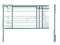
Revision history
Rev Date Description
04 20090826 LPC24XX user manual release.
Modifications:
• Memory size for LPC2458 external SRAM memory corrected in Table 2–14.
• Deep power-down mode functionality added (see Section 4–3.4 “Power control” and
Section 26–6.6 “Alarm output”).
• Register containing device revision added (implemented starting with revision C, see
Section 30–9.11
).
• XTAL1 input selection and PCB layout guidelines added (see Section 4–2.2).
• Editorial updates throughout the user manual.
• ISP1302 replaces ISP1301 in Section 15–6.
• UART fractional baud rate generator disabled in auto baud mode (see Section 16–4.10
and Section 17–4.14).
03 20090115 LPC24XX user manual release.
Modifications:
Description of AHB1 and AHB2 configuration registers updated.
02 20081219 LPC24XX user manual release.
Modifications:
• Added parts LPC2420.
• Editorial updates.
• AHB1 and AHB2 configuration registers added.
01 20080718 Initial LPC24XX user manual release. Replaces all draft versions UM10237_1.00 to
UM10237_1.05.

UM10237_4 © NXP B.V. 2009. All rights reserved.
User manual Rev. 04 — 26 August 2009 3 of 792
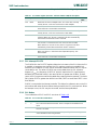
1. Introduction
NXP Semiconductor designed the LPC2400 microcontrollers around a 16-bit/32-bit
ARM7TDMI-S CPU core with real-time debug interfaces that include both JTAG and
embedded Trace. The LPC2400 microcontrollers have 512 kB of on-chip high-speed
Flash memory. This Flash memory includes a special 128-bit wide memory interface and
accelerator architecture that enables the CPU to execute sequential instructions from
Flash memory at the maximum 72 MHz system clock rate. This feature is available only
on the LPC2000 ARM Microcontroller family of products. The LPC2400 can execute both
32-bit ARM and 16-bit Thumb instructions. Support for the two Instruction Sets means
Engineers can choose to optimize their application for either performance or code size at
the sub-routine level. When the core executes instructions in Thumb state it can reduce
code size by more than 30 % with only a small loss in performance while executing
instructions in ARM state maximizes core performance.
The LPC2400 microcontrollers are ideal for multi-purpose communication applications. It
incorporates a 10/100 Ethernet Media Access Controller (MAC), a USB full speed
device/host/OTG controller with 4 kB of endpoint RAM, four UARTs, two Controller Area
Network (CAN) channels, an SPI interface, two Synchronous Serial Ports (SSP), three I
2
C
interfaces, and an I
2
S interface. Supporting this collection of serial communications
interfaces are the following feature components; an on-chip 4 MHz internal precision
oscillator, 98 kB of total RAM consisting of 64 kB of local SRAM, 16 kB SRAM for
Ethernet, 16 kB SRAM for general purpose DMA, 2 kB of battery powered SRAM, and an
External Memory Controller (EMC). These features make this device optimally suited for
communication gateways and protocol converters. Complementing the many serial
communication controllers, versatile clocking capabilities, and memory features are
various 32-bit timers, an improved 10-bit ADC, 10-bit DAC, two PWM units, four external
interrupt pins, and up to 160 fast GPIO lines. The LPC2400 connect 64 of the GPIO pins
to the hardware based Vector Interrupt Controller (VIC) that means these external inputs
can generate edge-triggered, interrupts. All of these features make the LPC2400
particularly suitable for industrial control and medical systems.
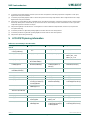
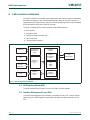
2. How to read this manual
Important: The term “LPC24XX“ in this user manual will be used as a generic name for all
LPC2400 parts. It covers the following parts: LPC2458, LPC2420, LPC2460, LPC2468,
LPC2470, and LPC2478.
For information about individual parts refer to Table 1–1
and Table 1–2.
UM10237
Chapter 1: LPC24XX Introductory information
Rev. 04 — 26 August 2009 User manual
Table 1. LPC24XX overview
LPC2458 LPC2420/60 LPC2468 LPC2470 LPC2478
Features Section 1–3
Section 1–3 Section 1–3 Section 1–3 Section 1–3
Ordering options Section 1–5.1 Section 1–5.2 Section 1–5.3 Section 1–5.4 Section 1–5.5
Block diagrams Section 1–9 Section 1–10 Section 1–11 Section 1–12 Section 1–13

UM10237_4 © NXP B.V. 2009. All rights reserved.
User manual Rev. 04 — 26 August 2009 4 of 792
NXP Semiconductors
UM10237
Chapter 1: LPC24XX Introductory information
Most features and peripherals are identical for all LPC2400 parts. All differences are listed
in Table 1–2
.
3. LPC2400 features
• ARM7TDMI-S processor, running at up to 72 MHz.
• 98 kB on-chip SRAM includes:
– 64 kB of SRAM on the ARM local bus for high performance CPU access.
– 16 kB SRAM for Ethernet interface. Can also be used as general purpose SRAM.
– 16 kB SRAM for general purpose DMA use also accessible by the USB.
– 2 kB SRAM data storage powered from the RTC power domain.
• LPC2458/68/78 only: 512 kB on-chip Flash program memory with In-System
Programming (ISP) and In-Application Programming (IAP) capabilities. Flash program
memory is on the ARM local bus for high performance CPU access.
• Dual Advanced High-performance Bus (AHB) system allows memory access by
multiple resources and simultaneous program execution with no contention.
• EMC provides support for asynchronous static memory devices such as RAM, ROM
and Flash, as well as dynamic memories such as Single Data Rate SDRAM.
• Advanced Vectored Interrupt Controller (VIC), supporting up to 32 vectored interrupts.
• General Purpose AHB DMA controller (GPDMA) that can be used with the SSP, I
2
S,
and SD/MM interface as well as for memory-to-memory transfers.
• LPC2470/78 only: LCD controller, supporting both Super-Twisted Nematic (STN) and
Thin-Film Transistors (TFT) displays.
– Dedicated DMA controller.
– Selectable display resolution (up to 1024 × 768 pixels).
– Supports up to 24-bit true-color mode.
• Serial Interfaces:
– Ethernet MAC with MII/RMII interface and associated DMA controller. These
functions reside on an independent AHB bus.
– USB 2.0 full-speed dual port device/host/OTG controller with on-chip PHY and
associated DMA controller.
– Four UARTs with fractional baud rate generation, one with modem control I/O, one
with IrDA support, all with FIFO.
– CAN controller with two channels.
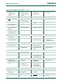
Table 2. Differences between LPC2400 parts
Pins/
High-speed
GPIO pins
Flash EMC LCD
LPC2458 180/136 512 kB 16-bit no
LPC2460/20 208/160 flashless 32-bit no
LPC2468 208/160 512 kB 32-bit no
LPC2470 208/160 flashless 32-bit yes
LPC2478 208/160 512 kB 32-bit yes

UM10237_4 © NXP B.V. 2009. All rights reserved.
User manual Rev. 04 — 26 August 2009 5 of 792
NXP Semiconductors
UM10237
Chapter 1: LPC24XX Introductory information
– SPI controller.
– Two SSP controllers, with FIFO and multi-protocol capabilities. One is an alternate
for the SPI port, sharing its interrupt. SSPs can be used with the GPDMA
controller.
– Three I
2
C-bus interfaces (one with open-drain and two with standard port pins).
– I
2
S (Inter-IC Sound) interface for digital audio input or output. It can be used with
the GPDMA.
• Other peripherals:
– SD/MMC memory card interface.
– 160 general purpose I/O pins with configurable pull-up/down resistors.
– 10-bit ADC with input multiplexing among 8 pins.
– 10-bit DAC.
– Four general purpose timers/counters with 8 capture inputs and 10 compare
outputs. Each timer block has an external count input.
– Two PWM/timer blocks with support for three-phase motor control. Each PWM has
an external count inputs.
– Real-Time Clock (RTC) with separate power domain, clock source can be the RTC
oscillator or the APB clock.
– 2 kB SRAM powered from the RTC power pin, allowing data to be stored when the
rest of the chip is powered off.
– WatchDog Timer (WDT). The WDT can be clocked from the internal RC oscillator,
the RTC oscillator, or the APB clock.
• Standard ARM test/debug interface for compatibility with existing tools.
• Emulation trace module supports real-time trace.
• Single 3.3 V power supply (3.0 V to 3.6 V).
• Four reduced power modes: idle, sleep, power-down, and deep power-down.
• Four external interrupt inputs configurable as edge/level sensitive. All pins on PORT0
and PORT2 can be used as edge sensitive interrupt sources.
• Processor wake-up from Power-down mode via any interrupt able to operate during
Power-down mode (includes external interrupts, RTC interrupt, USB activity, Ethernet
wake-up interrupt, CAN bus activity, PORT0/2 pin interrupt).
• Two independent power domains allow fine tuning of power consumption based on
needed features.
• Each peripheral has its own clock divider for further power saving. These dividers help
reducing active power by 20 - 30 %.
• Brownout detect with separate thresholds for interrupt and forced reset.
• On-chip power-on reset.
• On-chip crystal oscillator with an operating range of 1 MHz to 24 MHz.
• 4 MHz internal RC oscillator trimmed to 1 % accuracy that can optionally be used as
the system clock. When used as the CPU clock, does not allow CAN and USB to run.
• On-chip PLL allows CPU operation up to the maximum CPU rate without the need for
a high frequency crystal. May be run from the main oscillator, the internal RC
oscillator, or the RTC oscillator.

UM10237_4 © NXP B.V. 2009. All rights reserved.
User manual Rev. 04 — 26 August 2009 6 of 792
NXP Semiconductors
UM10237
Chapter 1: LPC24XX Introductory information
• Boundary scan for simplified board testing.
• Versatile pin function selections allow more possibilities for using on-chip peripheral
functions.
4. Applications
• Industrial control
• Medical systems
• Protocol converter
• Communications
5. Ordering options
5.1 LPC2458 ordering options
5.2 LPC2460 ordering options
Table 3. LPC2458 ordering information
Type number Package
Name Description Version
LPC2458FET180 TFBGA180 plastic thin fine-pitch ball grid array package; 180 balls; body 12 x 12 x 0.8 mm SOT570-2
Table 4. LPC2458 ordering options
Type number Flash
(kB)
SRAM (kB) External
bus
Ethernet USB
OTG/
OHC/
DEV
+4kB
FIFO
CAN channels
SD/
MMC
GP
DMA
ADC channels
DAC channels
Temp
range
Local bus
Ethernet buffer
GP/USB
RTC
Total
LPC2458FET180 512 64 16 16 2 98 16-bit MII/
RMII
yes 2 yes yes 8 1 −40 °C to
+85 °C
Table 5. LPC2420/60 ordering information
Type number Package
Name Description Version
LPC2420FBD208 LQFP208 plastic low profile quad flat package; 208 leads; body 28 × 28 × 1.4 mm SOT459-1
LPC2460FBD208 LQFP208 plastic low profile quad flat package; 208 leads; body 28 × 28 × 1.4 mm SOT459-1
LPC2460FET208 TFBGA208 plastic thin fine-pitch ball grid array package; 208 balls; body 15 × 15 × 0.7 mm SOT950-1

UM10237_4 © NXP B.V. 2009. All rights reserved.
User manual Rev. 04 — 26 August 2009 7 of 792
NXP Semiconductors
UM10237
Chapter 1: LPC24XX Introductory information
5.3 LPC2468 ordering options
5.4 LPC2470 ordering options
Table 6. LPC2420/60 ordering options
Type number Flash
(kB)
SRAM (kB) External
bus
Ethernet USB
OTG/
OHCI/
DEV
+4kB
FIFO
CAN channels
SD/
MMC
GP
DMA
ADC channels
DAC channels
Temp
range
Local bus
Ethernet buffer
GP/USB
RTC
Total
LPC2420FBD208 N/A 64 - 16 2 82 Full 32-bit - yes - yes yes 8 1 −40 °C to
+85 °C
LPC2460FBD208 N/A 64 16 16 2 98 Full 32-bit MII/RMII yes 2 yes yes 8 1 −40 °C to
+85 °C
LPC2460FET208 N/A 64 16 16 2 98 Full 32-bit MII/RMII yes 2 yes yes 8 1 −40 °C to
+85 °C
Table 7. LPC2468 ordering information
Type number Package
Name Description Version
LPC2468FBD208 LQFP208 plastic low profile quad flat package; 208 leads; body 28 × 28 × 1.4 mm SOT459-1
LPC2468FET208 TFBGA208 plastic thin fine-pitch ball grid array package; 208 balls; body 15 x 15 x 0.7 mm SOT950-1
Table 8. LPC2468 ordering options
Type number Flash
(kB)
SRAM (kB) External
bus
Ethernet USB
OTG/
OHC/
DEV
+ 4 kB
FIFO
CAN channels
SD/
MMC
GP
DMA
ADC channels
DAC channels
Temp
range
Local bus
Ethernet buffer
GP/USB
RTC
Total
LPC2468FBD208 512 64 16 16 2 98 Full 32-bit MII/
RMII
yes 2 yes yes 8 1 −40 °C to
+85 °C
LPC2468FET208 512 64 16 16 2 98 Full 32-bit MII/
RMII
yes 2 yes yes 8 1 −40 °C to
+85 °C
Table 9. LPC2470 ordering information
Type number Package
Name Description Version
LPC2470FBD208 LQFP208 plastic low profile quad flat package; 208 leads; body 28 × 28 × 1.4 mm SOT459-1
LPC2470FET208 TFBGA208 plastic thin fine-pitch ball grid array package; 208 balls; body 15 × 15 ×
0.7 mm
SOT950-1

UM10237_4 © NXP B.V. 2009. All rights reserved.
User manual Rev. 04 — 26 August 2009 8 of 792
NXP Semiconductors
UM10237
Chapter 1: LPC24XX Introductory information
5.5 LPC2478 ordering options
6. Architectural overview
The LPC2400 microcontroller consists of an ARM7TDMI-S CPU with emulation support,
the ARM7 local bus for closely coupled, high speed access to the majority of on-chip
memory, the AMBA AHB interfacing to high speed on-chip peripherals and external
memory, and the AMBA APB for connection to other on-chip peripheral functions. The
microcontroller permanently configures the ARM7TDMI-S processor for little-endian byte
order.
The LPC2400 implements two AHB buses in order to allow the Ethernet block to operate
without interference caused by other system activity. The primary AHB, referred to as
AHB1, includes the VIC, GPDMA controller, and EMC.
Table 10. LPC2470 ordering options
Type number Flash
(kB)
SRAM (kB) External
bus
Ethernet USB
OTG/
OHC/
Device
+ 4 kB
FIFO
CAN channels
SD/
MMC
GP
DMA
ADC channels
DAC channels
Temp
range
Local bus
Ethernet buffer
GP/USB
RTC
Total
LPC2470FBD208 N/A 64 16 16 2 98 Full
32-bit
MII/RMII yes 2 yes yes 8 1 −40 °C
to
+85 °C
LPC2470FET208 N/A 64 16 16 2 98 Full
32-bit
MII/RMII yes 2 yes yes 8 1 −40 °C
to
+85 °C
Table 11. LPC2478 ordering information
Type number Package
Name Description Version
LPC2478FBD208 LQFP208 plastic low profile quad flat package; 208 leads; body 28 × 28 × 1.4 mm SOT459-1
LPC2478FET208 TFBGA208 plastic thin fine-pitch ball grid array package; 208 balls; body 15 × 15 ×
0.7 mm
SOT950-1
Table 12. LPC2478 ordering options
Type number Flash
(kB)
SRAM (kB) External
bus
Ethernet USB
OTG/
OHC/
Device
+ 4 kB
FIFO
CAN channels
SD/
MMC
GP
DMA
ADC channels
DAC channels
Temp
range
Local bus
Ethernet buffer
GP/USB
RTC
Total
LPC2478FBD208 512 64 16 16 2 98 Full
32-bit
MII/RMII yes 2 yes yes 8 1 −40 °C
to
+85 °C
LPC2478FET208 512 64 16 16 2 98 Full
32-bit
MII/RMII yes 2 yes yes 8 1 −40 °C
to
+85 °C

UM10237_4 © NXP B.V. 2009. All rights reserved.
User manual Rev. 04 — 26 August 2009 9 of 792
NXP Semiconductors
UM10237
Chapter 1: LPC24XX Introductory information
The second AHB, referred to as AHB2, includes only the Ethernet block and an
associated 16 kB SRAM. In addition, a bus bridge is provided that allows the secondary
AHB to be a bus master on AHB1, allowing expansion of Ethernet buffer space into
off-chip memory or unused space in memory residing on AHB1.
In summary, bus masters with access to AHB1 are the ARM7 itself, the GPDMA function,
and the Ethernet block (via the bus bridge from AHB2). Bus masters with access to AHB2
are the ARM7 and the Ethernet block.
AHB peripherals are allocated a 2 MB range of addresses at the very top of the 4 GB
ARM memory space. Each AHB peripheral is allocated a 16 kB address space within the
AHB address space. Lower speed peripheral functions are connected to the APB bus.
The AHB to APB bridge interfaces the APB bus to the AHB bus. APB peripherals are also
allocated a 2 MB range of addresses, beginning at the 3.5 GB address point. Each APB
peripheral is allocated a 16 kB address space within the APB address space.
The ARM7TDMI-S processor is a general purpose 32-bit microprocessor, which offers
high performance and very low power consumption. The ARM architecture is based on
Reduced Instruction Set Computer (RISC) principles, and the instruction set and related
decode mechanism are much simpler than those of microprogrammed complex
instruction set computers. This simplicity results in a high instruction throughput and
impressive real-time interrupt response from a small and cost-effective processor core.
Pipeline techniques are employed so that all parts of the processing and memory systems
can operate continuously. Typically, while one instruction is being executed, its successor
is being decoded, and a third instruction is being fetched from memory.
The ARM7TDMI-S processor also employs a unique architectural strategy known as
Thumb, which makes it ideally suited to high-volume applications with memory
restrictions, or applications where code density is an issue.
The key idea behind Thumb is that of a super-reduced instruction set. Essentially, the
ARM7TDMI-S processor has two instruction sets:
• the standard 32-bit ARM set
• a 16-bit Thumb set
The Thumb set’s 16-bit instruction length allows it to approach higher density compared to
standard ARM code while retaining most of the ARM’s performance.
7. On-chip flash programming memory (LPC2458/68/78)
The LPC2400 incorporates 512 kB Flash memory system. This memory may be used for
both code and data storage. Programming of the Flash memory may be accomplished in
several ways. It may be programmed In System via the serial port (UART0). The
application program may also erase and/or program the Flash while the application is
running, allowing a great degree of flexibility for data storage field and firmware upgrades.
The Flash memory is 128 bits wide and includes pre-fetching and buffering techniques to
allow it to operate at speeds of 72 MHz.
The LPC2400 provides a minimum of 100000 write/erase cycles and 20 years of data
retention.

UM10237_4 © NXP B.V. 2009. All rights reserved.
User manual Rev. 04 — 26 August 2009 10 of 792
NXP Semiconductors
UM10237
Chapter 1: LPC24XX Introductory information
8. On-chip SRAM
The LPC2400 includes a SRAM memory of 64 kB reserved for the ARM processor
exclusive use. This RAM may be used for code and/or data storage and may be accessed
as 8 bits, 16 bits, and 32 bits.
A 16 kB SRAM block serving as a buffer for the Ethernet controller and a 16 kB SRAM
associated with the second AHB bus can be used both for data and code storage, too.
Remaining SRAM such as a 4 kB USB FIFO and a 2 kB RTC SRAM can be used for data
storage only. The RTC SRAM is battery powered and retains the content in the absence of
the main power supply.

UM10237_4 © NXP B.V. 2009. All rights reserved.
User manual Rev. 04 — 26 August 2009 11 of 792
NXP Semiconductors
UM10237
Chapter 1: LPC24XX Introductory information
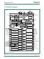
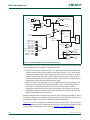
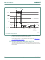
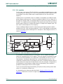
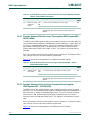
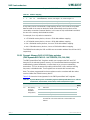
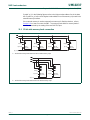
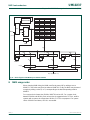
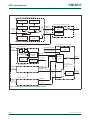
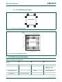
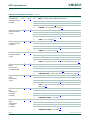
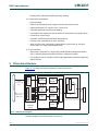
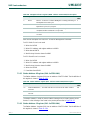
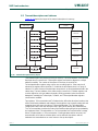
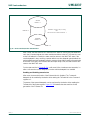
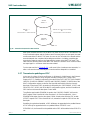
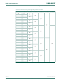
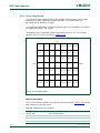
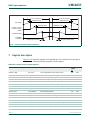
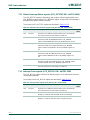
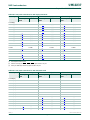
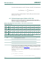
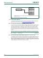
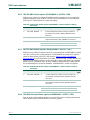
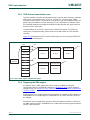
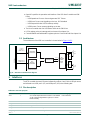
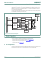
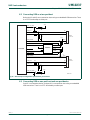
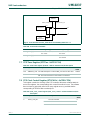
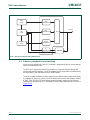
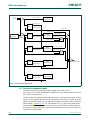
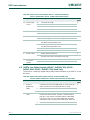
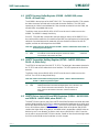
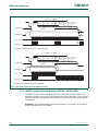
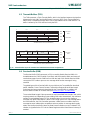
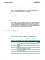
9. LPC2458 block diagram
Fig 1. LPC2458 block diagram
power domain 2
LPC2458
A[19:0]
D[15:0]
EXTERNAL
MEMORY
CONTROLLER
ALARM
002aad093
PWM0, PWM1
ARM7TDMI-S
PLL
EINT3 to EINT0
FLASH
P3, P4
P0, P1, P2,
LEGACY GPI/O
64 PINS TOTAL
P0, P1
SCK, SCK0
MOSI, MOSI0
SSEL, SSEL0
SCK1
MOSI1
MISO1
SSEL1
SCL0, SCL1, SCL2
I2SRX_CLK
I2STX_CLK
I2SRX_WS
I2STX_WS
8 × AD0
RTCX1
RTCX2
MCICLK, MCIPWR
RXD0, RXD2, RXD3
TXD1
RXD1
RD1, RD2
TD1, TD2
CAN1, CAN2
port 1
XTAL1
TCK TDO
EXTIN0
XTAL2
RESET
TRST
TDITMS
HIGH-SPEED
GPI/O
136 PINS
TOTAL
port 2
64 kB
SRAM
512 kB
FLASH
INTERNAL
CONTROLLERS
TEST/DEBUG
INTERFACE
EMULATION
TRACE MODULE
trace signals
AHB
BRIDGE
AHB
BRIDGE
ETHERNET
MAC WITH
DMA
16 kB
SRAM
MASTER
PORT
AHB TO
AHB BRIDGE
SLAVE
PORT
system
clock
SYSTEM
FUNCTIONS
INTERNAL RC
OSCILLATOR
V
DDA
V
DD(3V3)
V
DD(DCDC)(3V3)
VREF
V
SSA
, V
SSIO,
V
SSCORE
VIC
16 kB
SRAM
USB DEVICE/
HOST/OTG WITH
4 kB RAM AND DMA
GP DMA
CONTROLLER
I
2
S INTERFACE
SPI, SSP0 INTERFACE
I2SRX_SDA
I2STX_SDA
MISO, MISO0
SSP1 INTERFACE
SD/MMC CARD
INTERFACE
MCICMD,
MCIDAT[3:0]
TXD0, TXD2, TXD3
UART0, UART2, UART3
UART1
DTR1, RTS1
DSR1, CTS1, DCD1,
RI1
I
2
C0, I
2
C1, I
2
C2
SDA0, SDA1, SDA2
EXTERNAL INTERRUPTS
CAPTURE/COMPARE
TIMER0/TIMER1/
TIMER2/TIMER3
A/D CONVERTER
D/A CONVERTER
2 kB BATTERY RAM
RTC
OSCILLATOR
REAL-
TIME
CLOCK
WATCHDOG TIMER
SYSTEM CONTROL
2 × CAP0/CAP1/
CAP2/CAP3
4 × MAT2,
2 × MAT3,
2 × MAT1/MAT0
6 × PWM0, PWM1
1 × PCAP0,
2 × PCAP1
AOUT
VBAT
AHB TO
APB BRIDGE
SRAM
MII/RMII
V
BUS
DBGEN
P0, P2
AHB2
AHB1
control lines

UM10237_4 © NXP B.V. 2009. All rights reserved.
User manual Rev. 04 — 26 August 2009 12 of 792
NXP Semiconductors
UM10237
Chapter 1: LPC24XX Introductory information
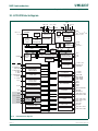
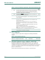
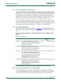
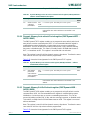
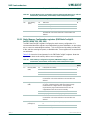
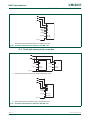
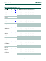
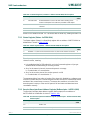
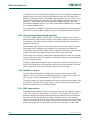
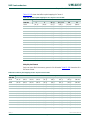
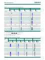
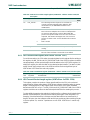
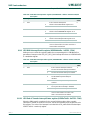
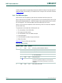
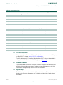
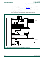
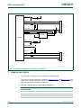
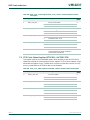
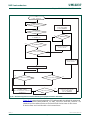
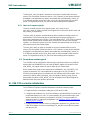
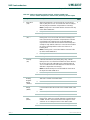
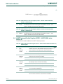
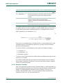
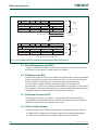
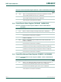
10. LPC2420/60 block diagram
(1) LPC2460 only.
Fig 2. LPC2460 block diagram
power domain 2
LPC2420/2460
A[23:0]
D[31:0]
EXTERNAL
MEMORY
CONTROLLER
ALARM
002aad313
PWM0, PWM1
ARM7TDMI-S
PLL
EINT3 to EINT0
P3, P4
P0, P1, P2,
LEGACY GPI/O
64 PINS TOTAL
P0, P1
SCK, SCK0
MOSI, MOSI0
SSEL, SSEL0
SCK1
MOSI1
MISO1
SSEL1
SCL0, SCL1, SCL2
I2SRX_CLK
I2STX_CLK
I2SRX_WS
I2STX_WS
8 × AD0
RTCX1
RTCX2
MCICLK, MCIPWR
RXD0, RXD2, RXD3
TXD1
RXD1
RD1, RD2
TD1, TD2
CAN1
(1)
, CAN2
(1)
port1
XTAL1
TCK TDO
EXTIN0
XTAL2
RESET
TRST
TDITMS
HIGH-SPEED
GPI/O
160 PINS
TOTAL
port2
64 kB
SRAM
INTERNAL
SRAM
CONTROLLER
TEST/DEBUG
INTERFACE
EMULATION
TRACE MODULE
trace signals
AHB
BRIDGE
AHB
BRIDGE
ETHERNET
MAC WITH
DMA
(1)
16 kB
SRAM
(1)
MASTER
PORT
AHB TO
AHB BRIDGE
SLAVE
PORT
system
clock
SYSTEM
FUNCTIONS
INTERNAL RC
OSCILLATOR
V
DDA
V
DD(3V3)
V
DD(DCDC)(3V3)
VREF
V
SSA
, V
SSCORE
, V
SSIO
VIC
16 kB
SRAM
USB DEVICE/
HOST/OTG WITH
4 kB RAM AND DMA
GP DMA
CONTROLLER
I
2
S INTERFACE
SPI, SSP0 INTERFACE
I2SRX_SDA
I2STX_SDA
MISO, MISO0
SSP1 INTERFACE
SD/MMC CARD
INTERFACE
MCICMD,
MCIDAT[3:0]
TXD0, TXD2, TXD3
UART0, UART2, UART3
UART1
DTR1, RTS1
DSR1, CTS1, DCD1,
RI1
I
2
C0, I
2
C1, I
2
C2
SDA0, SDA1, SDA2
EXTERNAL INTERRUPTS
CAPTURE/COMPARE
TIMER0/TIMER1/
TIMER2/TIMER3
A/D CONVERTER
D/A CONVERTER
2 kB BATTERY RAM
RTC
OSCILLATOR
REAL-
TIME
CLOCK
WATCHDOG TIMER
SYSTEM CONTROL
2 × CAP0/CAP1/
CAP2/CAP3
4 × MAT2/MAT3,
2 × MAT0,
3 × MAT1
6 × PWM0/PWM1
1 × PCAP0,
2 × PCAP1
AOUT
VBAT
AHB TO
APB BRIDGE
MII/RMII
V
BUS
DBGEN
P0, P2
AHB2
AHB1
control lines

UM10237_4 © NXP B.V. 2009. All rights reserved.
User manual Rev. 04 — 26 August 2009 13 of 792
NXP Semiconductors
UM10237
Chapter 1: LPC24XX Introductory information
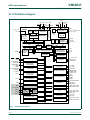
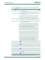
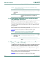
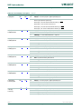
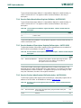
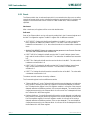
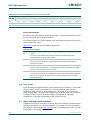
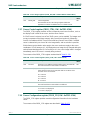
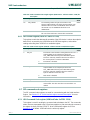
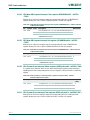
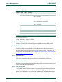
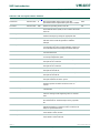
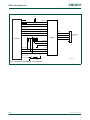
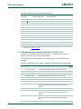
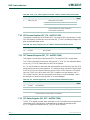
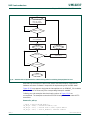
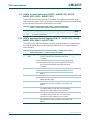
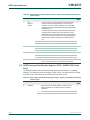
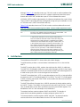
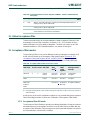
11. LPC2468 block diagram
Fig 3. LPC2468 block diagram
power domain 2
LPC2468
A[23:0]
D[31:0]
EXTERNAL
MEMORY
CONTROLLER
ALARM
002aac721
PWM0, PWM1
ARM7TDMI-S
PLL
EINT3 to EINT0
FLASH
P3, P4
P0, P1, P2,
LEGACY GPI/O
64 PINS TOTAL
P0, P1
SCK, SCK0
MOSI, MOSI0
SSEL, SSEL0
SCK1
MOSI1
MISO1
SSEL1
SCL0, SCL1, SCL2
I2SRX_CLK
I2STX_CLK
I2SRX_WS
I2STX_WS
8 × AD0
RTCX1
RTCX2
MCICLK, MCIPWR
RXD0, RXD2, RXD3
TXD1
RXD1
RD1, RD2
TD1, TD2
CAN1, CAN2
port1
XTAL1
TCK TDO
EXTIN0
XTAL2
RESET
TRST
TDITMS
HIGH-SPEED
GPI/O
160 PINS
TOTAL
port2
64 kB
SRAM
512 kB
FLASH
INTERNAL
CONTROLLERS
TEST/DEBUG
INTERFACE
EMULATION
TRACE MODULE
trace signals
AHB
BRIDGE
AHB
BRIDGE
ETHERNET
MAC WITH
DMA
16 kB
SRAM
MASTER
PORT
AHB TO
AHB BRIDGE
SLAVE
PORT
system
clock
SYSTEM
FUNCTIONS
INTERNAL RC
OSCILLATOR
V
DDA
V
DD(3V3)
V
DD(DCDC)(3V3)
VREF
V
SSA
, V
SSIO,
V
SSCORE
VIC
16 kB
SRAM
USB DEVICE/
HOST/OTG WITH
4 kB RAM AND DMA
GP DMA
CONTROLLER
I
2
S INTERFACE
SPI, SSP0 INTERFACE
I2SRX_SDA
I2STX_SDA
MISO, MISO0
SSP1 INTERFACE
SD/MMC CARD
INTERFACE
MCICMD,
MCIDAT[3:0]
TXD0, TXD2, TXD3
UART0, UART2, UART3
UART1
DTR1, RTS1
DSR1, CTS1, DCD1,
RI1
I
2
C0, I
2
C1, I
2
C2
SDA0, SDA1, SDA2
EXTERNAL INTERRUPTS
CAPTURE/COMPARE
TIMER0/TIMER1/
TIMER2/TIMER3
A/D CONVERTER
D/A CONVERTER
2 kB BATTERY RAM
RTC
OSCILLATOR
REAL-
TIME
CLOCK
WATCHDOG TIMER
SYSTEM CONTROL
2 × CAP0/CAP1/
CAP2/CAP3
4 × MAT2/MAT3,
2 × MAT0,
3 × MAT1
6 × PWM0/PWM1
1 × PCAP0,
2 × PCAP1
AOUT
VBAT
AHB TO
APB BRIDGE
SRAM
MII/RMII
V
BUS
DBGEN
P0, P2
AHB2
AHB1
control lines

UM10237_4 © NXP B.V. 2009. All rights reserved.
User manual Rev. 04 — 26 August 2009 14 of 792
NXP Semiconductors
UM10237
Chapter 1: LPC24XX Introductory information
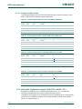
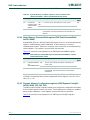
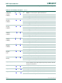
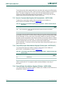
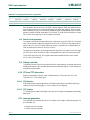
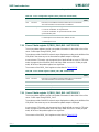
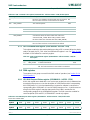
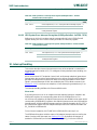
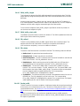
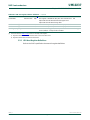
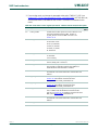
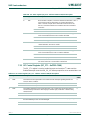
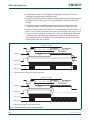
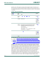
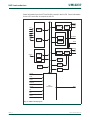
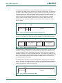
12. LPC2470 block diagram
Fig 4. LPC2470 block diagram
power domain 2
LPC2470
A[23:0]
D[31:0]
EXTERNAL
MEMORY
CONTROLLER
ALARM
002aad317
PWM0, PWM1
ARM7TDMI-S
PLL
EINT3 to EINT0
P3, P4
P0, P1, P2,
LEGACY GPI/O
64 PINS TOTAL
P0, P1
SCK, SCK0
3 × I2STX
3 × I2SRX
8 × LCD control
LCDVD[23:0]
LCDCLKIN
MOSI, MOSI0
SSEL, SSEL0
SCK1
MOSI1
MISO1
SSEL1
SCL0, SCL1, SCL2
8 × AD0
RTCX1
RTCX2
MCICLK, MCIPWR
RXD0, RXD2, RXD3
RD1, RD2
TD1, TD2
CAN1, CAN2
port1
XTAL1
TCK TDO
EXTIN0
XTAL2
RESET
TRST
TDITMS
HIGH-SPEED
GPI/O
160 PINS
TOTAL
port2
64 kB
SRAM
INTERNAL
SRAM
CONTROLLER
TEST/DEBUG
INTERFACE
EMULATION
TRACE MODULE
trace signals
AHB
BRIDGE
AHB
BRIDGE
ETHERNET
MAC WITH
DMA
16 kB
SRAM
MASTER
PORT
AHB TO
AHB BRIDGE
SLAVE
PORT
system
clock
SYSTEM
FUNCTIONS
INTERNAL RC
OSCILLATOR
V
DDA
V
DD(3V3)
V
DD(DCDC)(3V3)
VREF
VIC
16 kB
SRAM
USB DEVICE/
HOST/OTG WITH
4 kB RAM AND DMA
GP DMA
CONTROLLER
LCD INTERFACE
WITH DMA
I
2
S INTERFACE
SPI, SSP0 INTERFACE
MISO, MISO0
SSP1 INTERFACE
SD/MMC CARD
INTERFACE
MCICMD,
MCIDAT[3:0]
TXD0, TXD2, TXD3
UART0, UART2, UART3
UART1
TXD1, DTR1, RTS1
RXD1, DSR1, CTS1,
DCD1, RI1
I
2
C0, I
2
C1, I
2
C2
SDA0, SDA1, SDA2
EXTERNAL INTERRUPTS
CAPTURE/COMPARE
TIMER0/TIMER1/
TIMER2/TIMER3
A/D CONVERTER
D/A CONVERTER
2 kB BATTERY RAM
RTC
OSCILLATOR
REAL-
TIME
CLOCK
WATCHDOG TIMER
SYSTEM CONTROL
2 × CAP0/CAP1/
CAP2/CAP3
4 × MAT2/MAT3,
2 × MAT0,
3 × MAT1
6 × PWM0/PWM1
1 × PCAP0,
2 × PCAP1
AOUT
VBAT
AHB TO
APB BRIDGE
MII/RMII
V
BUS
DBGEN
P0, P2
AHB2
AHB1
control lines
V
SSA
, V
SSCORE
, V
SSIO

UM10237_4 © NXP B.V. 2009. All rights reserved.
User manual Rev. 04 — 26 August 2009 15 of 792
NXP Semiconductors
UM10237
Chapter 1: LPC24XX Introductory information
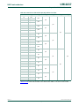
13. LPC2478 block diagram
Fig 5. LPC2478 block diagram
power domain 2
LPC2478
A[23:0]
D[31:0]
EXTERNAL
MEMORY
CONTROLLER
ALARM
002aac805
PWM0, PWM1
ARM7TDMI-S
PLL
EINT3 to EINT0
FLASH
P3, P4
P0, P1, P2,
LEGACY GPI/O
64 PINS TOTAL
P0, P1
SCK0, SCK
3 × I2STX
3 × I2SRX
8 × LCD control
LCDVD[23:0]
LCDCLKIN
MOSI0, MOSI
SSEL0, SSEL
SCK1
MOSI1
MISO1
SSEL1
SCL0, SCL1, SCL2
8 × AD0
RTCX1
RTCX2
MCICLK, MCIPWR
RXD0, RXD2, RXD3
RD1, RD2
TD1, TD2
CAN1, CAN2
port1
XTAL1
TCK TDO
EXTIN0
XTAL2
RESET
TRST
TDITMS
HIGH-SPEED
GPI/O
160 PINS
TOTAL
port2
64 kB
SRAM
512 kB
FLASH
INTERNAL
CONTROLLERS
TEST/DEBUG
INTERFACE
EMULATION
TRACE MODULE
trace signals
AHB
BRIDGE
AHB
BRIDGE
ETHERNET
MAC WITH
DMA
16 kB
SRAM
MASTER
PORT
AHB TO
AHB BRIDGE
SLAVE
PORT
system
clock
SYSTEM
FUNCTIONS
INTERNAL RC
OSCILLATOR
V
DDA
V
DD(3V3)
V
DD(DCDC)(3V3)
VREF
V
SSA
, V
SSIO,
V
SSCORE
VIC
16 kB
SRAM
USB DEVICE/
HOST/OTG WITH
4 kB RAM AND DMA
GP DMA
CONTROLLER
LCD INTERFACE
WITH DMA
I
2
S INTERFACE
SSP0/SPI INTERFACE
MISO0, MISO
SSP1 INTERFACE
SD/MMC CARD
INTERFACE
MCICMD,
MCIDAT[3:0]
TXD0, TXD2, TXD3
UART0, UART2, UART3
UART1
TXD1, DTR1, RTS1
RXD1, DSR1, CTS1,
DCD1, RI1
I
2
C0, I
2
C1, I
2
C2
SDA0, SDA1, SDA2
EXTERNAL INTERRUPTS
CAPTURE/COMPARE
TIMER0/TIMER1/
TIMER2/TIMER3
A/D CONVERTER
D/A CONVERTER
2 kB BATTERY RAM
RTC
OSCILLATOR
REAL-
TIME
CLOCK
WATCHDOG TIMER
SYSTEM CONTROL
2 × CAP0/CAP1/
CAP2/CAP3
4 × MAT2/MAT3,
2 × MAT0,
3 × MAT1
6 × PWM0/PWM1
1 × PCAP0,
2 × PCAP1
AOUT
VBAT
AHB TO
APB BRIDGE
SRAM
MII/RMII
V
BUS
DBGEN
P0, P2
AHB2
AHB1
control lines

UM10237_4 © NXP B.V. 2009. All rights reserved.
User manual Rev. 04 — 26 August 2009 16 of 792
1. How to read this chapter
The memory addressing and mapping for different LPC2400 parts depends on flash size,
EMC size, and the LCD peripheral, see Table 2–13
.
2. Memory map and peripheral addressing
ARM processors have a single 4 GB address space. The following table shows how this
space is used on NXP embedded ARM devices.
UM10237
Chapter 2: LPC24XX Memory mapping
Rev. 04 — 26 August 2009 User manual
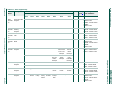
Table 13. LPC2400 memory options and addressing
Flash LCD EMC Memory map
Table 2–19;
Table 2–21
Figure 2–8
LPC2458 512 kB no 16-bit Table 2–14
LPC2420 flashless no 32-bit Table 2–15
LPC2460 flashless no 32-bit Table 2–15
LPC2468 512 kB no 32-bit Table 2–16
LPC2470 flashless yes 32-bit Table 2–15
LPC2478 512 kB yes 32-bit Table 2–16
Table 14. LPC2458 memory usage and details
Address range General use Address range details and description
0x0000 0000 to
0x3FFF FFFF
On-chip non-volatile
memory and Fast I/O
0x0000 0000 - 0x0007 FFFF Flash Memory (512 kB)
0x3FFF C000 - 0x3FFF FFFF Fast GPIO registers
0x4000 0000 to
0x7FFF FFFF
On-chip RAM 0x4000 0000 - 0x4000 FFFF RAM (64 kB)
0x7FE0 0000 - 0x7FE0 3FFF Ethernet RAM (16 kB)
0x7FD0 0000 - 0x7FD0 3FFF USB RAM (16 kB)
0x8000 0000 to
0xDFFF FFFF
Off-Chip Memory Two static memory banks, 1 MB each
0x8000 0000 - 0x800F FFFF Static memory bank 0
0x8100 0000 - 0x810F FFFF Static memory bank 1
Two dynamic memory banks, 256 MB each
0xA000 0000 - 0xAFFF FFFF Dynamic memory bank 0
0xB000 0000 - 0xBFFF FFFF Dynamic memory bank 1
0xE000 0000 to
0xEFFF FFFF
APB Peripherals 36 peripheral blocks, 16 kB each
0xF000 0000 to
0xFFFF FFFF
AHB peripherals

UM10237_4 © NXP B.V. 2009. All rights reserved.
User manual Rev. 04 — 26 August 2009 17 of 792
NXP Semiconductors
UM10237
Chapter 2: LPC24XX Memory mapping
Table 15. LPC2420/60/70 memory usage and details
Address range General use Address range details and description
0x0000 0000 to
0x3FFF FFFF
Fast I/O 0x0000 0000 - 0x0007 FFFF Reserved (flashless parts)
0x3FFF C000 - 0x3FFF FFFF Fast GPIO registers
0x4000 0000 to
0x7FFF FFFF
On-chip RAM 0x4000 0000 - 0x4000 FFFF RAM (64 kB)
0x7FE0 0000 - 0x7FE0 3FFF Ethernet RAM (16 kB) (LPC2460
only)
0x7FD0 0000 - 0x7FD0 3FFF USB RAM (16 kB)
0x8000 0000 to
0xDFFF FFFF
Off-Chip Memory Four static memory banks, 16 MB each
0x8000 0000 - 0x80FF FFFF Static memory bank 0
0x8100 0000 - 0x81FF FFFF Static memory bank 1
0x8200 0000 - 0x82FF FFFF Static memory bank 2
0x8300 0000 - 0x83FF FFFF Static memory bank 3
Four dynamic memory banks, 256 MB each
0xA000 0000 - 0xAFFF FFFF Dynamic memory bank 0
0xB000 0000 - 0xBFFF FFFF Dynamic memory bank 1
0xC000 0000 - 0xCFFF FFFF Dynamic memory bank 2
0xD000 0000 - 0xDFFF FFFF Dynamic memory bank 3
0xE000 0000 to
0xEFFF FFFF
APB Peripherals 36 peripheral blocks, 16 kB each
0xF000 0000 to
0xFFFF FFFF
AHB peripherals
Table 16. LPC2468/78 memory usage and details
Address range General use Address range details and description
0x0000 0000 to
0x3FFF FFFF
On-chip non-volatile
memory and Fast I/O
0x0000 0000 - 0x0007 FFFF Flash Memory (512 kB)
0x3FFF C000 - 0x3FFF FFFF Fast GPIO registers
0x4000 0000 to
0x7FFF FFFF
On-chip RAM 0x4000 0000 - 0x4000 FFFF RAM (64 kB)
0x7FE0 0000 - 0x7FE0 3FFF Ethernet RAM (16 kB)
0x7FD0 0000 - 0x7FD0 3FFF USB RAM (16 kB)
0x8000 0000 to
0xDFFF FFFF
Off-Chip Memory Four static memory banks, 16 MB each
0x8000 0000 - 0x80FF FFFF Static memory bank 0
0x8100 0000 - 0x81FF FFFF Static memory bank 1
0x8200 0000 - 0x82FF FFFF Static memory bank 2
0x8300 0000 - 0x83FF FFFF Static memory bank 3
Four dynamic memory banks, 256 MB each
0xA000 0000 - 0xAFFF FFFF Dynamic memory bank 0
0xB000 0000 - 0xBFFF FFFF Dynamic memory bank 1
0xC000 0000 - 0xCFFF FFFF Dynamic memory bank 2
0xD000 0000 - 0xDFFF FFFF Dynamic memory bank 3
0xE000 0000 to
0xEFFF FFFF
APB Peripherals 36 peripheral blocks, 16 kB each
0xF000 0000 to
0xFFFF FFFF
AHB peripherals

UM10237_4 © NXP B.V. 2009. All rights reserved.
User manual Rev. 04 — 26 August 2009 18 of 792
NXP Semiconductors
UM10237
Chapter 2: LPC24XX Memory mapping
3. Memory maps
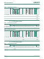
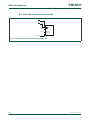
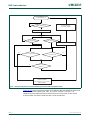
The LPC2400 incorporates several distinct memory regions, shown in the following
figures. Figure 2–6
shows the overall map of the entire address space from the user
program viewpoint following reset. The interrupt vector area supports address remapping,
which is described later in this section.
Fig 6. LPC2400 system memory map
0.0 GB
1.0 GB
ON-CHIP NON-VOLATILE MEMORY OR RESERVED
0x0000 0000
RESERVED ADDRESS SPACE
SPECIAL REGISTERS
ON-CHIP STATIC RAM
RESERVED ADDRESS SPACE
0x4000 0000
0x3FFF 8000
0x3FFF FFFF
2.0 GB 0x8000 0000
0x7FFF FFFF
BOOT ROM AND BOOT FLASH
EXTERNAL STATIC AND DYNAMIC MEMORY
3.75 GB
4.0 GB
3.5 GB
AHB PERIPHERALS
APB PERIPHERALS
0xE000 0000
0xF000 0000
0xFFFF FFFF

UM10237_4 © NXP B.V. 2009. All rights reserved.
User manual Rev. 04 — 26 August 2009 19 of 792
NXP Semiconductors
UM10237
Chapter 2: LPC24XX Memory mapping
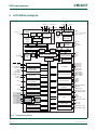
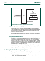
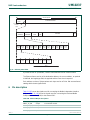
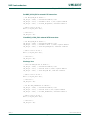
Figure 8 and Table 2–17 show different views of the peripheral address space. Both the
AHB and APB peripheral areas are 2 megabyte spaces which are divided up into 128
peripherals. Each peripheral space is 16 kilobytes in size. This allows simplifying the
address decoding for each peripheral.
Fig 7. Peripheral memory map
RESERVED
RESERVED
0xF000 0000
0xEFFF FFFF
APB PERIPHERALS
0xE020 0000
0xE01F FFFF
0xE000 0000
AHB PERIPHERALS
0xFFFF FFFF
0xFFE0 0000
0xFFDF FFFF
3.75 GB
3.5 GB
3.5 GB + 2 MB
4.0 GB - 2 MB
4.0 GB

UM10237_4 © NXP B.V. 2009. All rights reserved.
User manual Rev. 04 — 26 August 2009 20 of 792
NXP Semiconductors
UM10237
Chapter 2: LPC24XX Memory mapping
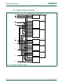
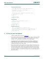
All peripheral register addresses are word aligned (to 32 bit boundaries) regardless of
their size. This eliminates the need for byte lane mapping hardware that would be required
to allow byte (8 bit) or half-word (16 bit) accesses to occur at smaller boundaries. An
implication of this is that word and half-word registers must be accessed all at once. For
example, it is not possible to read or write the upper byte of a word register separately.
(1) LPC247x only.
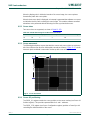
Fig 8. AHB peripheral map
VECTORED INTERRUPT CONTROLLER
(AHB PERIPHERAL #0)
0xFFFF F000 (4G - 4K)
0xFFFF C000
0xFFFF 8000
(AHB PERIPHERAL #4)
(AHB PERIPHERAL #3)
(AHB PERIPHERAL #2)
(AHB PERIPHERAL #1)
(AHB PERIPHERAL #126)
0xFFE1 8000
0xFFE1 4000
0xFFE1 0000
0xFFE0 C000
0xFFE0 8000
0xFFE0 4000
0xFFE0 0000
ETHERNET CONTROLLER
GENERAL PURPOSE DMA CONTROLLER
EXTERNAL MEMORY CONTROLLER
USB CONTROLLER
LCD
(1)
(AHB PERIPHERAL #5)
NOT USED
Page is loading ...
Page is loading ...
Page is loading ...
Page is loading ...
Page is loading ...
Page is loading ...
Page is loading ...
Page is loading ...
Page is loading ...
Page is loading ...
Page is loading ...
Page is loading ...
Page is loading ...
Page is loading ...
Page is loading ...
Page is loading ...
Page is loading ...
Page is loading ...
Page is loading ...
Page is loading ...
Page is loading ...
Page is loading ...
Page is loading ...
Page is loading ...
Page is loading ...
Page is loading ...
Page is loading ...
Page is loading ...
Page is loading ...
Page is loading ...
Page is loading ...
Page is loading ...
Page is loading ...
Page is loading ...
Page is loading ...
Page is loading ...
Page is loading ...
Page is loading ...
Page is loading ...
Page is loading ...
Page is loading ...
Page is loading ...
Page is loading ...
Page is loading ...
Page is loading ...
Page is loading ...
Page is loading ...
Page is loading ...
Page is loading ...
Page is loading ...
Page is loading ...
Page is loading ...
Page is loading ...
Page is loading ...
Page is loading ...
Page is loading ...
Page is loading ...
Page is loading ...
Page is loading ...
Page is loading ...
Page is loading ...
Page is loading ...
Page is loading ...
Page is loading ...
Page is loading ...
Page is loading ...
Page is loading ...
Page is loading ...
Page is loading ...
Page is loading ...
Page is loading ...
Page is loading ...
Page is loading ...
Page is loading ...
Page is loading ...
Page is loading ...
Page is loading ...
Page is loading ...
Page is loading ...
Page is loading ...
Page is loading ...
Page is loading ...
Page is loading ...
Page is loading ...
Page is loading ...
Page is loading ...
Page is loading ...
Page is loading ...
Page is loading ...
Page is loading ...
Page is loading ...
Page is loading ...
Page is loading ...
Page is loading ...
Page is loading ...
Page is loading ...
Page is loading ...
Page is loading ...
Page is loading ...
Page is loading ...
Page is loading ...
Page is loading ...
Page is loading ...
Page is loading ...
Page is loading ...
Page is loading ...
Page is loading ...
Page is loading ...
Page is loading ...
Page is loading ...
Page is loading ...
Page is loading ...
Page is loading ...
Page is loading ...
Page is loading ...
Page is loading ...
Page is loading ...
Page is loading ...
Page is loading ...
Page is loading ...
Page is loading ...
Page is loading ...
Page is loading ...
Page is loading ...
Page is loading ...
Page is loading ...
Page is loading ...
Page is loading ...
Page is loading ...
Page is loading ...
Page is loading ...
Page is loading ...
Page is loading ...
Page is loading ...
Page is loading ...
Page is loading ...
Page is loading ...
Page is loading ...
Page is loading ...
Page is loading ...
Page is loading ...
Page is loading ...
Page is loading ...
Page is loading ...
Page is loading ...
Page is loading ...
Page is loading ...
Page is loading ...
Page is loading ...
Page is loading ...
Page is loading ...
Page is loading ...
Page is loading ...
Page is loading ...
Page is loading ...
Page is loading ...
Page is loading ...
Page is loading ...
Page is loading ...
Page is loading ...
Page is loading ...
Page is loading ...
Page is loading ...
Page is loading ...
Page is loading ...
Page is loading ...
Page is loading ...
Page is loading ...
Page is loading ...
Page is loading ...
Page is loading ...
Page is loading ...
Page is loading ...
Page is loading ...
Page is loading ...
Page is loading ...
Page is loading ...
Page is loading ...
Page is loading ...
Page is loading ...
Page is loading ...
Page is loading ...
Page is loading ...
Page is loading ...
Page is loading ...
Page is loading ...
Page is loading ...
Page is loading ...
Page is loading ...
Page is loading ...
Page is loading ...
Page is loading ...
Page is loading ...
Page is loading ...
Page is loading ...
Page is loading ...
Page is loading ...
Page is loading ...
Page is loading ...
Page is loading ...
Page is loading ...
Page is loading ...
Page is loading ...
Page is loading ...
Page is loading ...
Page is loading ...
Page is loading ...
Page is loading ...
Page is loading ...
Page is loading ...
Page is loading ...
Page is loading ...
Page is loading ...
Page is loading ...
Page is loading ...
Page is loading ...
Page is loading ...
Page is loading ...
Page is loading ...
Page is loading ...
Page is loading ...
Page is loading ...
Page is loading ...
Page is loading ...
Page is loading ...
Page is loading ...
Page is loading ...
Page is loading ...
Page is loading ...
Page is loading ...
Page is loading ...
Page is loading ...
Page is loading ...
Page is loading ...
Page is loading ...
Page is loading ...
Page is loading ...
Page is loading ...
Page is loading ...
Page is loading ...
Page is loading ...
Page is loading ...
Page is loading ...
Page is loading ...
Page is loading ...
Page is loading ...
Page is loading ...
Page is loading ...
Page is loading ...
Page is loading ...
Page is loading ...
Page is loading ...
Page is loading ...
Page is loading ...
Page is loading ...
Page is loading ...
Page is loading ...
Page is loading ...
Page is loading ...
Page is loading ...
Page is loading ...
Page is loading ...
Page is loading ...
Page is loading ...
Page is loading ...
Page is loading ...
Page is loading ...
Page is loading ...
Page is loading ...
Page is loading ...
Page is loading ...
Page is loading ...
Page is loading ...
Page is loading ...
Page is loading ...
Page is loading ...
Page is loading ...
Page is loading ...
Page is loading ...
Page is loading ...
Page is loading ...
Page is loading ...
Page is loading ...
Page is loading ...
Page is loading ...
Page is loading ...
Page is loading ...
Page is loading ...
Page is loading ...
Page is loading ...
Page is loading ...
Page is loading ...
Page is loading ...
Page is loading ...
Page is loading ...
Page is loading ...
Page is loading ...
Page is loading ...
Page is loading ...
Page is loading ...
Page is loading ...
Page is loading ...
Page is loading ...
Page is loading ...
Page is loading ...
Page is loading ...
Page is loading ...
Page is loading ...
Page is loading ...
Page is loading ...
Page is loading ...
Page is loading ...
Page is loading ...
Page is loading ...
Page is loading ...
Page is loading ...
Page is loading ...
Page is loading ...
Page is loading ...
Page is loading ...
Page is loading ...
Page is loading ...
Page is loading ...
Page is loading ...
Page is loading ...
Page is loading ...
Page is loading ...
Page is loading ...
Page is loading ...
Page is loading ...
Page is loading ...
Page is loading ...
Page is loading ...
Page is loading ...
Page is loading ...
Page is loading ...
Page is loading ...
Page is loading ...
Page is loading ...
Page is loading ...
Page is loading ...
Page is loading ...
Page is loading ...
Page is loading ...
Page is loading ...
Page is loading ...
Page is loading ...
Page is loading ...
Page is loading ...
Page is loading ...
Page is loading ...
Page is loading ...
Page is loading ...
Page is loading ...
Page is loading ...
Page is loading ...
Page is loading ...
Page is loading ...
Page is loading ...
Page is loading ...
Page is loading ...
Page is loading ...
Page is loading ...
Page is loading ...
Page is loading ...
Page is loading ...
Page is loading ...
Page is loading ...
Page is loading ...
Page is loading ...
Page is loading ...
Page is loading ...
Page is loading ...
Page is loading ...
Page is loading ...
Page is loading ...
Page is loading ...
Page is loading ...
Page is loading ...
Page is loading ...
Page is loading ...
Page is loading ...
Page is loading ...
Page is loading ...
Page is loading ...
Page is loading ...
Page is loading ...
Page is loading ...
Page is loading ...
Page is loading ...
Page is loading ...
Page is loading ...
Page is loading ...
Page is loading ...
Page is loading ...
Page is loading ...
Page is loading ...
Page is loading ...
Page is loading ...
Page is loading ...
Page is loading ...
Page is loading ...
Page is loading ...
Page is loading ...
Page is loading ...
Page is loading ...
Page is loading ...
Page is loading ...
Page is loading ...
Page is loading ...
Page is loading ...
Page is loading ...
Page is loading ...
Page is loading ...
Page is loading ...
Page is loading ...
Page is loading ...
Page is loading ...
Page is loading ...
Page is loading ...
Page is loading ...
Page is loading ...
Page is loading ...
Page is loading ...
Page is loading ...
Page is loading ...
Page is loading ...
Page is loading ...
Page is loading ...
Page is loading ...
Page is loading ...
Page is loading ...
Page is loading ...
Page is loading ...
Page is loading ...
Page is loading ...
Page is loading ...
Page is loading ...
Page is loading ...
Page is loading ...
Page is loading ...
Page is loading ...
Page is loading ...
Page is loading ...
Page is loading ...
Page is loading ...
Page is loading ...
Page is loading ...
Page is loading ...
Page is loading ...
Page is loading ...
Page is loading ...
Page is loading ...
Page is loading ...
Page is loading ...
Page is loading ...
Page is loading ...
Page is loading ...
Page is loading ...
Page is loading ...
Page is loading ...
Page is loading ...
Page is loading ...
Page is loading ...
Page is loading ...
Page is loading ...
Page is loading ...
Page is loading ...
Page is loading ...
Page is loading ...
Page is loading ...
Page is loading ...
Page is loading ...
Page is loading ...
Page is loading ...
Page is loading ...
Page is loading ...
Page is loading ...
Page is loading ...
Page is loading ...
Page is loading ...
Page is loading ...
Page is loading ...
Page is loading ...
Page is loading ...
Page is loading ...
Page is loading ...
Page is loading ...
Page is loading ...
Page is loading ...
Page is loading ...
Page is loading ...
Page is loading ...
Page is loading ...
Page is loading ...
Page is loading ...
Page is loading ...
Page is loading ...
Page is loading ...
Page is loading ...
Page is loading ...
Page is loading ...
Page is loading ...
Page is loading ...
Page is loading ...
Page is loading ...
Page is loading ...
Page is loading ...
Page is loading ...
Page is loading ...
Page is loading ...
Page is loading ...
Page is loading ...
Page is loading ...
Page is loading ...
Page is loading ...
Page is loading ...
Page is loading ...
Page is loading ...
Page is loading ...
Page is loading ...
Page is loading ...
Page is loading ...
Page is loading ...
Page is loading ...
Page is loading ...
Page is loading ...
Page is loading ...
Page is loading ...
Page is loading ...
Page is loading ...
Page is loading ...
Page is loading ...
Page is loading ...
Page is loading ...
Page is loading ...
Page is loading ...
Page is loading ...
Page is loading ...
Page is loading ...
Page is loading ...
Page is loading ...
Page is loading ...
Page is loading ...
Page is loading ...
Page is loading ...
Page is loading ...
Page is loading ...
Page is loading ...
Page is loading ...
Page is loading ...
Page is loading ...
Page is loading ...
Page is loading ...
Page is loading ...
Page is loading ...
Page is loading ...
Page is loading ...
Page is loading ...
Page is loading ...
Page is loading ...
Page is loading ...
Page is loading ...
Page is loading ...
Page is loading ...
Page is loading ...
Page is loading ...
Page is loading ...
Page is loading ...
Page is loading ...
Page is loading ...
Page is loading ...
Page is loading ...
Page is loading ...
Page is loading ...
Page is loading ...
Page is loading ...
Page is loading ...
Page is loading ...
Page is loading ...
Page is loading ...
Page is loading ...
Page is loading ...
Page is loading ...
Page is loading ...
Page is loading ...
Page is loading ...
Page is loading ...
Page is loading ...
Page is loading ...
Page is loading ...
Page is loading ...
Page is loading ...
Page is loading ...
Page is loading ...
Page is loading ...
Page is loading ...
Page is loading ...
Page is loading ...
Page is loading ...
Page is loading ...
Page is loading ...
Page is loading ...
Page is loading ...
Page is loading ...
Page is loading ...
Page is loading ...
Page is loading ...
Page is loading ...
Page is loading ...
Page is loading ...
Page is loading ...
Page is loading ...
Page is loading ...
Page is loading ...
Page is loading ...
Page is loading ...
Page is loading ...
Page is loading ...
Page is loading ...
Page is loading ...
Page is loading ...
Page is loading ...
Page is loading ...
Page is loading ...
Page is loading ...
Page is loading ...
Page is loading ...
Page is loading ...
Page is loading ...
Page is loading ...
Page is loading ...
Page is loading ...
Page is loading ...
Page is loading ...
Page is loading ...
Page is loading ...
Page is loading ...
Page is loading ...
Page is loading ...
Page is loading ...
Page is loading ...
Page is loading ...
Page is loading ...
Page is loading ...
Page is loading ...
Page is loading ...
Page is loading ...
Page is loading ...
Page is loading ...
Page is loading ...
Page is loading ...
Page is loading ...
Page is loading ...
Page is loading ...
Page is loading ...
Page is loading ...
Page is loading ...
Page is loading ...
Page is loading ...
Page is loading ...
Page is loading ...
Page is loading ...
Page is loading ...
Page is loading ...
Page is loading ...
Page is loading ...
Page is loading ...
Page is loading ...
Page is loading ...
Page is loading ...
Page is loading ...
Page is loading ...
Page is loading ...
Page is loading ...
Page is loading ...
Page is loading ...
Page is loading ...
Page is loading ...
Page is loading ...
Page is loading ...
Page is loading ...
Page is loading ...
Page is loading ...
Page is loading ...
Page is loading ...
Page is loading ...
Page is loading ...
Page is loading ...
Page is loading ...
Page is loading ...
Page is loading ...
Page is loading ...
Page is loading ...
Page is loading ...
Page is loading ...
Page is loading ...
Page is loading ...
Page is loading ...
Page is loading ...
Page is loading ...
Page is loading ...
Page is loading ...
Page is loading ...
Page is loading ...
Page is loading ...
Page is loading ...
Page is loading ...
Page is loading ...
Page is loading ...
Page is loading ...
Page is loading ...
Page is loading ...
Page is loading ...
Page is loading ...
Page is loading ...
Page is loading ...
Page is loading ...
Page is loading ...
Page is loading ...
Page is loading ...
Page is loading ...
Page is loading ...
Page is loading ...
Page is loading ...
Page is loading ...
Page is loading ...
Page is loading ...
Page is loading ...
Page is loading ...
Page is loading ...
Page is loading ...
Page is loading ...
Page is loading ...
Page is loading ...
Page is loading ...
Page is loading ...
Page is loading ...
Page is loading ...
Page is loading ...
Page is loading ...
Page is loading ...
Page is loading ...
Page is loading ...
Page is loading ...
Page is loading ...
Page is loading ...
Page is loading ...
Page is loading ...
Page is loading ...
Page is loading ...
Page is loading ...
Page is loading ...
Page is loading ...
Page is loading ...
Page is loading ...
Page is loading ...
Page is loading ...
Page is loading ...
Page is loading ...
Page is loading ...
Page is loading ...
Page is loading ...
Page is loading ...
Page is loading ...
Page is loading ...
Page is loading ...
Page is loading ...
Page is loading ...
Page is loading ...
Page is loading ...
Page is loading ...
-
 1
1
-
 2
2
-
 3
3
-
 4
4
-
 5
5
-
 6
6
-
 7
7
-
 8
8
-
 9
9
-
 10
10
-
 11
11
-
 12
12
-
 13
13
-
 14
14
-
 15
15
-
 16
16
-
 17
17
-
 18
18
-
 19
19
-
 20
20
-
 21
21
-
 22
22
-
 23
23
-
 24
24
-
 25
25
-
 26
26
-
 27
27
-
 28
28
-
 29
29
-
 30
30
-
 31
31
-
 32
32
-
 33
33
-
 34
34
-
 35
35
-
 36
36
-
 37
37
-
 38
38
-
 39
39
-
 40
40
-
 41
41
-
 42
42
-
 43
43
-
 44
44
-
 45
45
-
 46
46
-
 47
47
-
 48
48
-
 49
49
-
 50
50
-
 51
51
-
 52
52
-
 53
53
-
 54
54
-
 55
55
-
 56
56
-
 57
57
-
 58
58
-
 59
59
-
 60
60
-
 61
61
-
 62
62
-
 63
63
-
 64
64
-
 65
65
-
 66
66
-
 67
67
-
 68
68
-
 69
69
-
 70
70
-
 71
71
-
 72
72
-
 73
73
-
 74
74
-
 75
75
-
 76
76
-
 77
77
-
 78
78
-
 79
79
-
 80
80
-
 81
81
-
 82
82
-
 83
83
-
 84
84
-
 85
85
-
 86
86
-
 87
87
-
 88
88
-
 89
89
-
 90
90
-
 91
91
-
 92
92
-
 93
93
-
 94
94
-
 95
95
-
 96
96
-
 97
97
-
 98
98
-
 99
99
-
 100
100
-
 101
101
-
 102
102
-
 103
103
-
 104
104
-
 105
105
-
 106
106
-
 107
107
-
 108
108
-
 109
109
-
 110
110
-
 111
111
-
 112
112
-
 113
113
-
 114
114
-
 115
115
-
 116
116
-
 117
117
-
 118
118
-
 119
119
-
 120
120
-
 121
121
-
 122
122
-
 123
123
-
 124
124
-
 125
125
-
 126
126
-
 127
127
-
 128
128
-
 129
129
-
 130
130
-
 131
131
-
 132
132
-
 133
133
-
 134
134
-
 135
135
-
 136
136
-
 137
137
-
 138
138
-
 139
139
-
 140
140
-
 141
141
-
 142
142
-
 143
143
-
 144
144
-
 145
145
-
 146
146
-
 147
147
-
 148
148
-
 149
149
-
 150
150
-
 151
151
-
 152
152
-
 153
153
-
 154
154
-
 155
155
-
 156
156
-
 157
157
-
 158
158
-
 159
159
-
 160
160
-
 161
161
-
 162
162
-
 163
163
-
 164
164
-
 165
165
-
 166
166
-
 167
167
-
 168
168
-
 169
169
-
 170
170
-
 171
171
-
 172
172
-
 173
173
-
 174
174
-
 175
175
-
 176
176
-
 177
177
-
 178
178
-
 179
179
-
 180
180
-
 181
181
-
 182
182
-
 183
183
-
 184
184
-
 185
185
-
 186
186
-
 187
187
-
 188
188
-
 189
189
-
 190
190
-
 191
191
-
 192
192
-
 193
193
-
 194
194
-
 195
195
-
 196
196
-
 197
197
-
 198
198
-
 199
199
-
 200
200
-
 201
201
-
 202
202
-
 203
203
-
 204
204
-
 205
205
-
 206
206
-
 207
207
-
 208
208
-
 209
209
-
 210
210
-
 211
211
-
 212
212
-
 213
213
-
 214
214
-
 215
215
-
 216
216
-
 217
217
-
 218
218
-
 219
219
-
 220
220
-
 221
221
-
 222
222
-
 223
223
-
 224
224
-
 225
225
-
 226
226
-
 227
227
-
 228
228
-
 229
229
-
 230
230
-
 231
231
-
 232
232
-
 233
233
-
 234
234
-
 235
235
-
 236
236
-
 237
237
-
 238
238
-
 239
239
-
 240
240
-
 241
241
-
 242
242
-
 243
243
-
 244
244
-
 245
245
-
 246
246
-
 247
247
-
 248
248
-
 249
249
-
 250
250
-
 251
251
-
 252
252
-
 253
253
-
 254
254
-
 255
255
-
 256
256
-
 257
257
-
 258
258
-
 259
259
-
 260
260
-
 261
261
-
 262
262
-
 263
263
-
 264
264
-
 265
265
-
 266
266
-
 267
267
-
 268
268
-
 269
269
-
 270
270
-
 271
271
-
 272
272
-
 273
273
-
 274
274
-
 275
275
-
 276
276
-
 277
277
-
 278
278
-
 279
279
-
 280
280
-
 281
281
-
 282
282
-
 283
283
-
 284
284
-
 285
285
-
 286
286
-
 287
287
-
 288
288
-
 289
289
-
 290
290
-
 291
291
-
 292
292
-
 293
293
-
 294
294
-
 295
295
-
 296
296
-
 297
297
-
 298
298
-
 299
299
-
 300
300
-
 301
301
-
 302
302
-
 303
303
-
 304
304
-
 305
305
-
 306
306
-
 307
307
-
 308
308
-
 309
309
-
 310
310
-
 311
311
-
 312
312
-
 313
313
-
 314
314
-
 315
315
-
 316
316
-
 317
317
-
 318
318
-
 319
319
-
 320
320
-
 321
321
-
 322
322
-
 323
323
-
 324
324
-
 325
325
-
 326
326
-
 327
327
-
 328
328
-
 329
329
-
 330
330
-
 331
331
-
 332
332
-
 333
333
-
 334
334
-
 335
335
-
 336
336
-
 337
337
-
 338
338
-
 339
339
-
 340
340
-
 341
341
-
 342
342
-
 343
343
-
 344
344
-
 345
345
-
 346
346
-
 347
347
-
 348
348
-
 349
349
-
 350
350
-
 351
351
-
 352
352
-
 353
353
-
 354
354
-
 355
355
-
 356
356
-
 357
357
-
 358
358
-
 359
359
-
 360
360
-
 361
361
-
 362
362
-
 363
363
-
 364
364
-
 365
365
-
 366
366
-
 367
367
-
 368
368
-
 369
369
-
 370
370
-
 371
371
-
 372
372
-
 373
373
-
 374
374
-
 375
375
-
 376
376
-
 377
377
-
 378
378
-
 379
379
-
 380
380
-
 381
381
-
 382
382
-
 383
383
-
 384
384
-
 385
385
-
 386
386
-
 387
387
-
 388
388
-
 389
389
-
 390
390
-
 391
391
-
 392
392
-
 393
393
-
 394
394
-
 395
395
-
 396
396
-
 397
397
-
 398
398
-
 399
399
-
 400
400
-
 401
401
-
 402
402
-
 403
403
-
 404
404
-
 405
405
-
 406
406
-
 407
407
-
 408
408
-
 409
409
-
 410
410
-
 411
411
-
 412
412
-
 413
413
-
 414
414
-
 415
415
-
 416
416
-
 417
417
-
 418
418
-
 419
419
-
 420
420
-
 421
421
-
 422
422
-
 423
423
-
 424
424
-
 425
425
-
 426
426
-
 427
427
-
 428
428
-
 429
429
-
 430
430
-
 431
431
-
 432
432
-
 433
433
-
 434
434
-
 435
435
-
 436
436
-
 437
437
-
 438
438
-
 439
439
-
 440
440
-
 441
441
-
 442
442
-
 443
443
-
 444
444
-
 445
445
-
 446
446
-
 447
447
-
 448
448
-
 449
449
-
 450
450
-
 451
451
-
 452
452
-
 453
453
-
 454
454
-
 455
455
-
 456
456
-
 457
457
-
 458
458
-
 459
459
-
 460
460
-
 461
461
-
 462
462
-
 463
463
-
 464
464
-
 465
465
-
 466
466
-
 467
467
-
 468
468
-
 469
469
-
 470
470
-
 471
471
-
 472
472
-
 473
473
-
 474
474
-
 475
475
-
 476
476
-
 477
477
-
 478
478
-
 479
479
-
 480
480
-
 481
481
-
 482
482
-
 483
483
-
 484
484
-
 485
485
-
 486
486
-
 487
487
-
 488
488
-
 489
489
-
 490
490
-
 491
491
-
 492
492
-
 493
493
-
 494
494
-
 495
495
-
 496
496
-
 497
497
-
 498
498
-
 499
499
-
 500
500
-
 501
501
-
 502
502
-
 503
503
-
 504
504
-
 505
505
-
 506
506
-
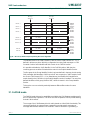 507
507
-
 508
508
-
 509
509
-
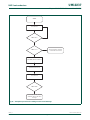 510
510
-
 511
511
-
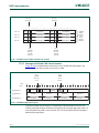 512
512
-
 513
513
-
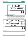 514
514
-
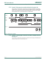 515
515
-
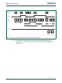 516
516
-
 517
517
-
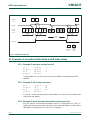 518
518
-
 519
519
-
 520
520
-
 521
521
-
 522
522
-
 523
523
-
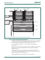 524
524
-
 525
525
-
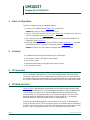 526
526
-
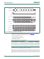 527
527
-
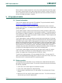 528
528
-
 529
529
-
 530
530
-
 531
531
-
 532
532
-
 533
533
-
 534
534
-
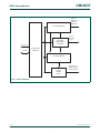 535
535
-
 536
536
-
 537
537
-
 538
538
-
 539
539
-
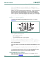 540
540
-
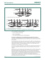 541
541
-
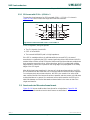 542
542
-
 543
543
-
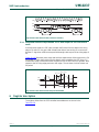 544
544
-
 545
545
-
 546
546
-
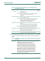 547
547
-
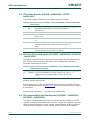 548
548
-
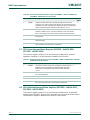 549
549
-
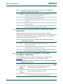 550
550
-
 551
551
-
 552
552
-
 553
553
-
 554
554
-
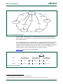 555
555
-
 556
556
-
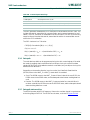 557
557
-
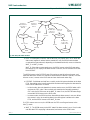 558
558
-
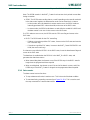 559
559
-
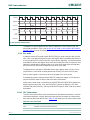 560
560
-
 561
561
-
 562
562
-
 563
563
-
 564
564
-
 565
565
-
 566
566
-
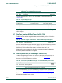 567
567
-
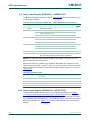 568
568
-
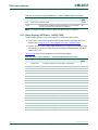 569
569
-
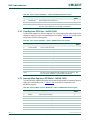 570
570
-
 571
571
-
 572
572
-
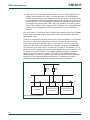 573
573
-
 574
574
-
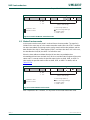 575
575
-
 576
576
-
 577
577
-
 578
578
-
 579
579
-
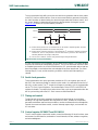 580
580
-
 581
581
-
 582
582
-
 583
583
-
 584
584
-
 585
585
-
 586
586
-
 587
587
-
 588
588
-
 589
589
-
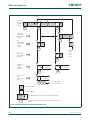 590
590
-
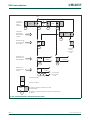 591
591
-
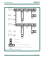 592
592
-
 593
593
-
 594
594
-
 595
595
-
 596
596
-
 597
597
-
 598
598
-
 599
599
-
 600
600
-
 601
601
-
 602
602
-
 603
603
-
 604
604
-
 605
605
-
 606
606
-
 607
607
-
 608
608
-
 609
609
-
 610
610
-
 611
611
-
 612
612
-
 613
613
-
 614
614
-
 615
615
-
 616
616
-
 617
617
-
 618
618
-
 619
619
-
 620
620
-
 621
621
-
 622
622
-
 623
623
-
 624
624
-
 625
625
-
 626
626
-
 627
627
-
 628
628
-
 629
629
-
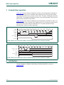 630
630
-
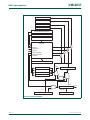 631
631
-
 632
632
-
 633
633
-
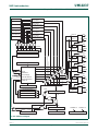 634
634
-
 635
635
-
 636
636
-
 637
637
-
 638
638
-
 639
639
-
 640
640
-
 641
641
-
 642
642
-
 643
643
-
 644
644
-
 645
645
-
 646
646
-
 647
647
-
 648
648
-
 649
649
-
 650
650
-
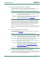 651
651
-
 652
652
-
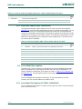 653
653
-
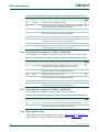 654
654
-
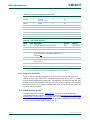 655
655
-
 656
656
-
 657
657
-
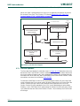 658
658
-
 659
659
-
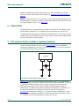 660
660
-
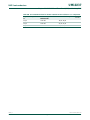 661
661
-
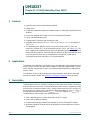 662
662
-
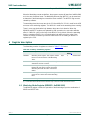 663
663
-
 664
664
-
 665
665
-
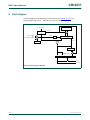 666
666
-
 667
667
-
 668
668
-
 669
669
-
 670
670
-
 671
671
-
 672
672
-
 673
673
-
 674
674
-
 675
675
-
 676
676
-
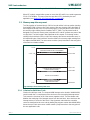 677
677
-
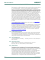 678
678
-
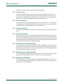 679
679
-
 680
680
-
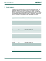 681
681
-
 682
682
-
 683
683
-
 684
684
-
 685
685
-
 686
686
-
 687
687
-
 688
688
-
 689
689
-
 690
690
-
 691
691
-
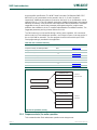 692
692
-
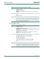 693
693
-
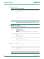 694
694
-
 695
695
-
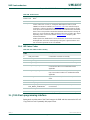 696
696
-
 697
697
-
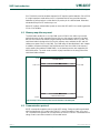 698
698
-
 699
699
-
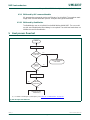 700
700
-
 701
701
-
 702
702
-
 703
703
-
 704
704
-
 705
705
-
 706
706
-
 707
707
-
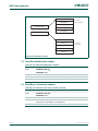 708
708
-
 709
709
-
 710
710
-
 711
711
-
 712
712
-
 713
713
-
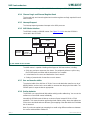 714
714
-
 715
715
-
 716
716
-
 717
717
-
 718
718
-
 719
719
-
 720
720
-
 721
721
-
 722
722
-
 723
723
-
 724
724
-
 725
725
-
 726
726
-
 727
727
-
 728
728
-
 729
729
-
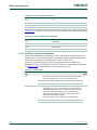 730
730
-
 731
731
-
 732
732
-
 733
733
-
 734
734
-
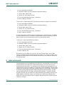 735
735
-
 736
736
-
 737
737
-
 738
738
-
 739
739
-
 740
740
-
 741
741
-
 742
742
-
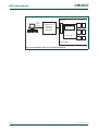 743
743
-
 744
744
-
 745
745
-
 746
746
-
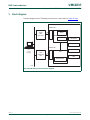 747
747
-
 748
748
-
 749
749
-
 750
750
-
 751
751
-
 752
752
-
 753
753
-
 754
754
-
 755
755
-
 756
756
-
 757
757
-
 758
758
-
 759
759
-
 760
760
-
 761
761
-
 762
762
-
 763
763
-
 764
764
-
 765
765
-
 766
766
-
 767
767
-
 768
768
-
 769
769
-
 770
770
-
 771
771
-
 772
772
-
 773
773
-
 774
774
-
 775
775
-
 776
776
-
 777
777
-
 778
778
-
 779
779
-
 780
780
-
 781
781
-
 782
782
-
 783
783
-
 784
784
-
 785
785
-
 786
786
-
 787
787
-
 788
788
-
 789
789
-
 790
790
-
 791
791
-
 792
792


NXP LPC2478FBD208 User guide
- Type
- User guide
- This manual is also suitable for
Ask a question and I''ll find the answer in the document
Finding information in a document is now easier with AI
Related papers
Other documents
-
NXP Semiconductors UM10237 User manual
-
Silicon Labs EFM32WG Reference guide
-
Digi NS9750 User manual
-
Maverick EP7312 User manual
-
Analog Devices ADuCM320 Hardware Reference Manual
-
 Cypress CY7C64113C User manual
-
Texas Instruments OMAP5912 Multimedia Processor Display Interface Reference (Rev. B) User guide
-
Intel PXA26X User manual
-
Intellisystem IT-232-CAN Owner's manual
-
