PN7462 Reference POS Application
All information provided in this document is subject to legal disclaimers.
© NXP Semiconductors N.V. 2017. All rights reserved.
User manual
COMPANY PUBLIC
Rev. 1.1 — 24 January 2017
353611
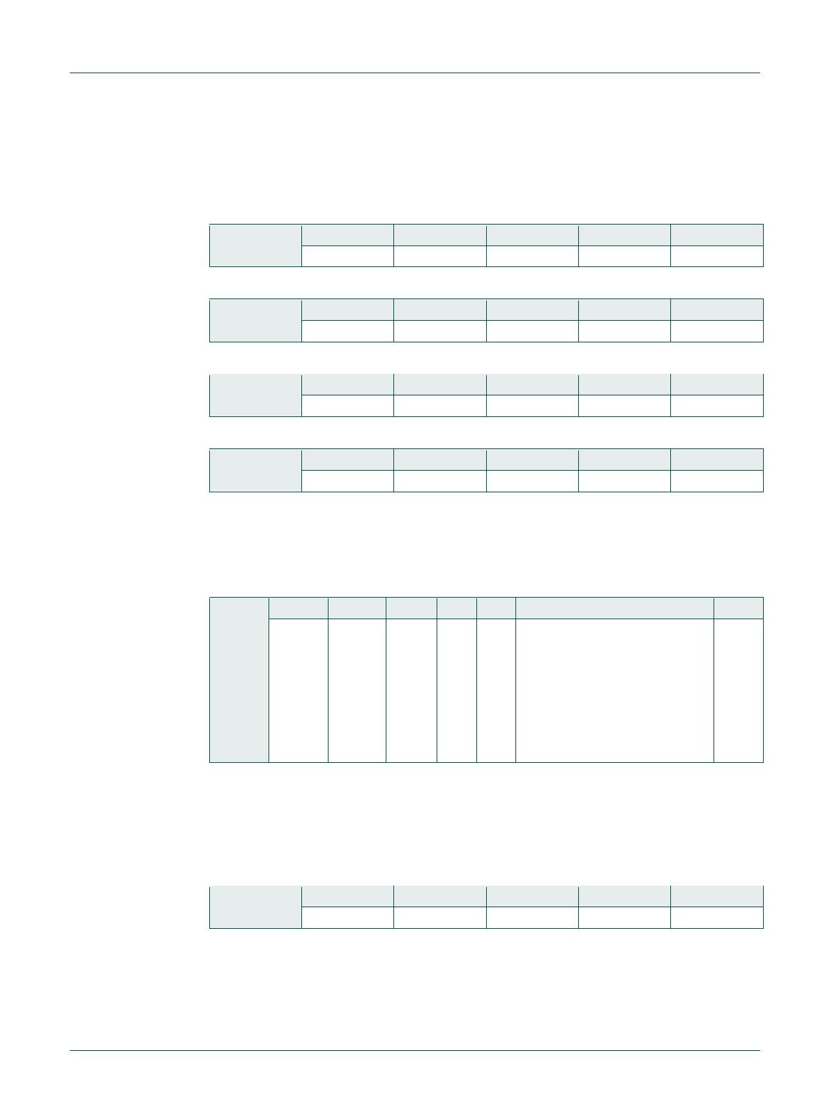
Read record commands
Read record commands are used to read the record in a card. Number of records varies
from card to card. Below a few records.
Table 10. Read record command for SFI2 Record 1
Payload
Table 11. Read record command for SFI3 Record 1
Payload
Table 12. Read record command for SFI4 Record 1
Payload
Table 13. Read record command for SFI4 Record 2
Payload
Generate AC command
This command generates the authentication parameters.
Table 14. Generate AC command
Payload
0x00, 0x00, 0x00, 0x00, 0x02,
0x00, 0x00, 0x00, 0x00, 0x00,
0x00, 0x00, 0x00, 0x56, 0x00,
0x00, 0x00, 0x00, 0x00, 0x09,
0x78, 0x14, 0x08, 0x13, 0x00,
0x45, 0x11, 0x15, 0x61, 0x23,
0x00, 0x00, 0x00, 0x00, 0x00,
0x00, 0x00, 0x00, 0x00, 0x00,
0x3F, 0x00, 0x00
Deactivate card command
This command informs the PN7462 to deactivate the card after the generated AC
command is successful.
Table 15. Deactivate card command
Payload


