NXP PN736X User guide

Type
User guide

This manual is also suitable for

UM10883
PN7462 family Quick Start Guide - Development Kit
Rev. 1.614 May 2018
319816
User manual
COMPANY PUBLIC
Document information
Info
Keywords
functional description of the customer board, NFC Cockpit
Abstract
describes PN7462 software stack, gives directions to run example
application using the MCUXpresso IDE. Document provides PN7462
customer board configuration instructions, gives board hardware
overview and provides basic steps how to use NFC Cockpit application.
NXP Semiconductors
UM10883
PN7462 family Quick Start Guide - Development Kit
UM10883
All information provided in this document is subject to legal disclaimers.
© NXP B.V. 2018. All rights reserved.
User manual
COMPANY PUBLIC
Rev. 1.614 May 2018
319816
2 of 120
Contact information
For more information, please visit:
http://www.nxp.com
Revision history
Rev
Date
Description
1.6
20180514
Added OM27462CDKP and PNEV7462C description, editorial changes
1.5
20180115
Reworked NFC Cockpit usage description
1.4
20170907
Updated Getting started description
PN7462 plugin for MCUXpresso not needed form version 10.0.2
Reworked NFC Cockpit installation description
1.3
20170511
Development Kit description added
MCUXpresso IDE support added
Board description and schematic updated
SW examples description updated
Abbreviation section added
1.2
20170216
PNEV7462B customer demo board V2.2 added
SW examples description updated
Guidelines how to upgrade firmware are updated
Figures updated
1.1
20161124
SW examples description updated
Guidelines how to import projects are updated
Figures updated
1.0
20160329
First release
NXP Semiconductors
UM10883
PN7462 family Quick Start Guide - Development Kit
UM10883
All information provided in this document is subject to legal disclaimers.
© NXP B.V. 2018. All rights reserved.
User manual
COMPANY PUBLIC
Rev. 1.614 May 2018
319816
3 of 120
1. Getting started
This document gives information about how to start software and hardware development
with PN7462 NFC Controller Development Kits: OM27462CDK [1] and OM27462CDKP
[2]. Development kit ensures easy and quick development of NFC applications running
on the PN7462 family [3] derivates. This guide gives extensive kit hardware overview and
describes board configuration options.
Document further describes PN7462AU FW and SW examples package. It gives step by
step instruction to install MCUXpresso IDE [4] and to run example application. It is also
provided extensive introduction to the PN7462 family software stack [5] and describes
each example in detail.
Finally, document describes NFC Cockpit [6], custom Windows application used in
prototyping and optimization.
In this document the terms „MIFARE DESFire card“, „MIFARE Classic card“ and
„MIFARE Ultralight card“ refer either to a MIFARE DESFire IC-based contactless card, a
MIFARE Classic IC-based contactless card or a MIFARE UItralight IC-based contactless
card.
1.1 Introduction to PN7462 NFC Controller Development Kits
Both, the OM27462CDK and the OM27462CDKP development kits are parts of the
PN7462 family product support package. Development Kits are designed to demonstrate
all functionalities of the PN7462 family and easies development of customized
applications and antenna design.
1.1.1 OM27462CDK
OM27462CDK Development Kit is based on the PNEV7462B board. Content of the
Development Kit is displayed on the following picture.
Fig 1. OM27462CDK Development Kit
NXP Semiconductors
UM10883
PN7462 family Quick Start Guide - Development Kit
UM10883
All information provided in this document is subject to legal disclaimers.
© NXP B.V. 2018. All rights reserved.
User manual
COMPANY PUBLIC
Rev. 1.614 May 2018
319816
4 of 120
Development Kit contains:
(1) PNEV7462B board with standard 65x65mm antenna
(2) 30x50mm antenna with matching components
(3) 3 PCBs for individual antenna matching
(4) Sample NFC cards and tags
(5) 2 USB cables; A to mini and A to micro
(6) 10 PN7462 samples
(7) 7.5V DC power supply
(8) LPC-Link 2 debug adapter (OM13054)
1.1.2 OM27462CDKP
OM27462CDKP Development Kit is based on the PNEV7462C board. Content of the
Development Kit is displayed on the following picture.
Fig 2. OM27462CDKP Development Kit
Development Kit contains:
(1) PNEV7462C board with standard 65x65mm antenna
(2) 30x50mm antenna with matching components
(3) 3 x PCBs for individual antenna matching
(4) Sample NFC cards and tags
(5) 2 x USB cables: A to mini and A to micro
(6) 5 x PN7462AU samples (HVQFN64)
NXP Semiconductors
UM10883
PN7462 family Quick Start Guide - Development Kit
UM10883
All information provided in this document is subject to legal disclaimers.
© NXP B.V. 2018. All rights reserved.
User manual
COMPANY PUBLIC
Rev. 1.614 May 2018
319816
5 of 120
(7) LPC-Link 2 debug adapter (OM13054)
(1) Control Panel\Hardware and Sound\Devices and Printers
Fig 3. Properly enumerated USB CCID reader
At this point a favorite PC/SC application can be started and tested with cards contained
in the kit.
NXP Semiconductors
UM10883
PN7462 family Quick Start Guide - Development Kit
UM10883
All information provided in this document is subject to legal disclaimers.
© NXP B.V. 2018. All rights reserved.
User manual
COMPANY PUBLIC
Rev. 1.614 May 2018
319816
6 of 120
2. Hardware overview of the PNEV7462B board
2.1 PNEV7462B concept
The basic concept of the PNEV7462B board is to enable hardware and software
evaluation of typical PN7462 family design and to support prototyping own antenna
circuitry. The supporting NFC Cockpit tool enables antenna tuning, DPC calibration and
the related TX and RX optimization in run time.
After successful optimization, register settings can be stored in the PN7462AU EEPROM
as well as saved in configuration file and used as input in design time.
PN7462AU FW and SW Examples available on the product page, ranging from POS
demo, contact and contactless CCID reader, P2P application, NFC forum related
examples, are customized primarily for PNEV7462B/C board and supported by
MCUXpresso, Keil or IAR development tools.
2.2 PNEV7462B board
Fig 4. PNEV7462B board
The board consists of the following blocks:
(1) PN7462AU circuitry with reset and download pushbuttons,
(2) External power supply connector (5.5/2.1 socket) and power supply selector,
(3) LDO regulator circuit for 3.3V and 5V
(4) LPCXpresso m-bed expansion circuit
(5) TDA8026 multiple smart card interface circuit
(6) Antenna coil and related matching circuit (marked in green and orange)
(7) Smart card socket (main slot on bottom PCB layer) and SIM size slots on top layer
(8) 65x65mm antenna coil
(9) 10-pin Cortex debug connector
(10) 26-pin shroud GPIO header and USB micro B female connector
8
7
6
1
9
4
5
10
11
2
3
NXP Semiconductors
UM10883
PN7462 family Quick Start Guide - Development Kit
UM10883
All information provided in this document is subject to legal disclaimers.
© NXP B.V. 2018. All rights reserved.
User manual
COMPANY PUBLIC
Rev. 1.614 May 2018
319816
7 of 120
(11) Diagnostic LED block connected to PN7462AU
2.2.1 Power circuitry
The power circuit consists of the power socket, diode bridge, selection jumper JP41 and
two low dropout linear voltage regulators. Power options include USB and LPC-Link 2 but
for the best performance external power source is recommended.
Note:
PN7462B v2.1: external power supply 7.5V max.
PN7462B v2.2: external power supply 13.5V max.
(2) USB supply, external supply & and LPC supply
Fig 5. PNEV7462B supply
2.2.2 PN7462AU block
The main part on the evaluation board is PN7462AU. It features a 32-bit ARM Cortex-
M0-based NFC microcontroller offering a one chip solution to build contact and
contactless applications.
Key features are:
20 MHz Cortex-M0 core
- 80/160 kB Flash, 12 kB RAM, 4 kB EEPROM
State-of-the-art RF interface: Full NFC, EMVCo 2.6
- Read/Write, Card Emulation & Peer-to-Peer Modes
- Transmitter current up to 250 mA
- Full MIFARE family support,
DPC for optimized antenna performance
Extensive host and peripheral interfaces
- Host/slave & master interfaces: I2C, SPI, USB, HSUART, I2CM, SPIM
- Optional contact interface (PN7462): UART, ISO/IEC 7816, EMVCo 4.3
- 12 to 21 GPIOs
NXP Semiconductors
UM10883
PN7462 family Quick Start Guide - Development Kit
UM10883
All information provided in this document is subject to legal disclaimers.
© NXP B.V. 2018. All rights reserved.
User manual
COMPANY PUBLIC
Rev. 1.614 May 2018
319816
8 of 120
Fig 6. PNEV7462B board schematic (PN7462 part)
2.2.3 LPCXpresso block
This block provides expansion interface for LPCXpresso MCU board providing standard
LPCXpresso/m-bed expansion connector (DIL54). LPCXpresso SPIM and I2CM
interfaces are routed to the PN7462AU host interface selector.
Additionally, board features a USB micro B connector (X1) routed to the LPC board USB
interface and the LPC board reset circuit. Diagnostic LED1-4 are connected to LPC port
pins.
NXP Semiconductors
UM10883
PN7462 family Quick Start Guide - Development Kit
UM10883
All information provided in this document is subject to legal disclaimers.
© NXP B.V. 2018. All rights reserved.
User manual
COMPANY PUBLIC
Rev. 1.614 May 2018
319816
9 of 120
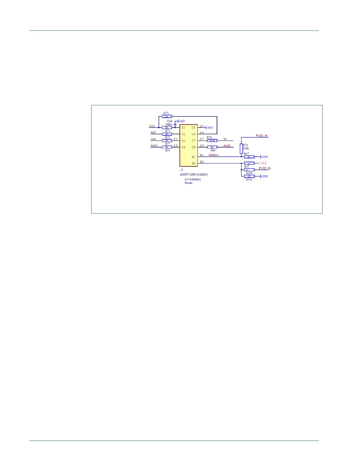
2.2.4 Smartcard interface
The PN7462AU integrates contact interface to enable communication with ISO7816 and
EMVCo contact smart cards, without the need for an external contact front end. It offers a
high level of security for the cards by performing current limitation, short-circuit detection,
ESD protection as well as supply supervision. Card slot/contactor is located on the board
bottom layer.
(1) Default setting for present pin (K1) is low active
Fig 7. PNEV7462B contact slot interface
2.2.5 TDA SAM extension interfaces
The PN7462AU can handle more than one smart card by controlling an extra contact
interface TDA8026 product from NXP. In this use case, the PN7462AU is the main
controller for the electrical and protocol part for the main card slot, while the secondary
slots are electrically controlled by an extra contact front-end interface (TDA), the
PN7462AU being the protocol controller for these extra slots. TDA8026 I2C port is
connected to the PN7462 I2CM to enable IC configuration.
In this case, several smart cards can be activated at the same time, but the
communication with each smart card has to go sequentially: it is not possible to
communicate with two smart cards at the same time as there is only one protocol control
block for all cards.
TDA8026 is required to handle the smart card electrical interface. The connection
between the PN7462AU and the TDA is composed of 2 channels:
- The host interface control, where the PN7462AU is the master, controlling the
TDA behavior: card activation, deactivation, TDA configuration (voltage level,
clock division, slew rates…)
- The ISO7816 link: the PN7462AU handles the ISO7816 communication protocol
and uses the TDA as a level shifter for the clock and I/O signals.
NXP Semiconductors
UM10883
PN7462 family Quick Start Guide - Development Kit
UM10883
All information provided in this document is subject to legal disclaimers.
© NXP B.V. 2018. All rights reserved.
User manual
COMPANY PUBLIC
Rev. 1.614 May 2018
319816
10 of 120
(1) 2 optional SAM slots can be assembled
Fig 8. PNEV7462B TDA8026 part schematics
NXP Semiconductors
UM10883
PN7462 family Quick Start Guide - Development Kit
UM10883
All information provided in this document is subject to legal disclaimers.
© NXP B.V. 2018. All rights reserved.
User manual
COMPANY PUBLIC
Rev. 1.614 May 2018
319816
11 of 120
2.2.6 Antenna coil and related matching circuit
In general, there are two antenna tunings possible with PNEV7462B board:
- asymmetrical
- symmetrical
The asymmetrical tuning is the standard tuning as taken from the existing NXP NFC
frontend design recommendations. It uses EMC cut off frequencies >17MHz, which
results in an asymmetrical transfer function, but shows a good detuning and loading
behavior. The asymmetrical transfer function has some disadvantages regarding the
pulse shapes and receiver performance, and requires a slightly reduced Q factor of the
antenna coil circuit itself.
Symmetrical coupling is used with DPC (Dynamic Power Control) feature of the PN7462
and offers an improved overall RF performance. This requires the antenna to be
“symmetrically” tuned and it requires the AGC to correlate with the driver current ITVDD.
and it requires the dynamic power control to be properly calibrated. The DPC Antenna
tuning (“symmetrical tuning with DPC) combines the advantages of enough field strength
at 4cm with the automatic power control to limit the maximum field strength at a close
distance. This tuning assures passing related EMVCo tests.
2.2.6.1 Default board antenna
Default 65x65 mm board antenna is designed to use symmetrical tuning (see Fig 9). This
antenna is not an optimal antenna as such, but intends to demonstrate the performance
and register settings of the PN7462 under typical design constraints like LCD or another
metallic object (e.g. PCB) inside the antenna area. Inside of the antenna area is filed of
10x10 fields simulating metallic object in real application.
NXP Semiconductors
UM10883
PN7462 family Quick Start Guide - Development Kit
UM10883
All information provided in this document is subject to legal disclaimers.
© NXP B.V. 2018. All rights reserved.
User manual
COMPANY PUBLIC
Rev. 1.614 May 2018
319816
12 of 120
Fig 9. Default 65x65 antenna matching diagram - symmetrical
The antenna connection uses the standard tuning circuit Fig 10. The EMC filter is
typically a second order low pass filter as shown in Fig 18, and contains an inductor (L0)
and a capacitor (C0). The cut off frequency defines the overall detuning behavior as well
as the transfer function of the antenna circuit. For symmetrical (DPC) tuning, EMC filter is
designed with a cut off frequency of f
EMC
= 14,8 MHz, and the antenna impedance is
tuned to Z = 20Ω.
(1) Standard tuning circuit
Fig 10. Matching circuit principle
NXP Semiconductors
UM10883
PN7462 family Quick Start Guide - Development Kit
UM10883
All information provided in this document is subject to legal disclaimers.
© NXP B.V. 2018. All rights reserved.
User manual
COMPANY PUBLIC
Rev. 1.614 May 2018
319816
13 of 120
(1) The matching components might be adapted due to antenna layout changes.
Fig 11. Antenna and matching
Table 1 lists components for the “symmetric” matching.
Table 1. Assembled matching components
General component
Component
PNEV7462B
Value
Comment
L0
L4/ L7
470nH
PNEV7462B V2.1->
0603LS-471NXJBC
PNEV7462B V2.2->
36502AR47JTDG
C0
C28/ C31
100pF
C0 split in 3 parallel
capacitors
C29/ C32
27pF
C38/ C44
120pF
C1
C35/ C49
33pF
NXP Semiconductors
UM10883
PN7462 family Quick Start Guide - Development Kit
UM10883
All information provided in this document is subject to legal disclaimers.
© NXP B.V. 2018. All rights reserved.
User manual
COMPANY PUBLIC
Rev. 1.614 May 2018
319816
14 of 120
General component
Component
PNEV7462B
Value
Comment
C37/ C47
1pF
C1 split in 2 parallel
capacitors
C2
1
C40/ C46
120pF
C2
2
C41/ C43
68pF
R
s
R117/ R119
2,2Ω
R
s
split in 2 parallel
resistors
R118/ R120
2,2Ω
Note: Without proper DPC calibration the loading and detuning might exceed the ITVDD
limit, if the symmetrical tuning is used. This might destroy the NFC reader IC
2.2.6.2 PCB for individual antenna matching
Development kit contains 3 PCB boards for individual antenna matching. This boards are
intended for prototyping custom asymmetrical or symmetrical (DPC) antenna design.
Default matching circuit can be replaced by individual antenna matching PCB.
2.3 PNEV7462B board available versions
Following Versions of the PNEV7462B board are available
PNEV7462B V2.1
PNEV7462B V2.2
2.3.1 PNEV7462B V2.1
The V2.1 of the customer evaluation board is the initial version of the board that comes
with the launch of the PN7462AU chip.
Fig 12. PNEV746B V2.1
NXP Semiconductors
UM10883
PN7462 family Quick Start Guide - Development Kit
UM10883
All information provided in this document is subject to legal disclaimers.
© NXP B.V. 2018. All rights reserved.
User manual
COMPANY PUBLIC
Rev. 1.614 May 2018
319816
15 of 120
2.3.2 PNEV7462B V2.2
The V2.2 of the customer evaluation board is the replacement and latest version of the
customer evaluation board incl. FCC certification. Functionality of the V2.2 is the same
as of V2.1.
Fig 13. PNEV7462B V2.2
Design changes V2.1 to V2.2:
External supply maximum value increased from 7.5V to12V
Different routing (PNEV7462B V2.1 stays the board reference design which can be
obtained from the NXP DocStore [8]). Layout recommendations for NFC readers can
be found in AN11090.
Changed EMC filter components
NXP Semiconductors
UM10883
PN7462 family Quick Start Guide - Development Kit
UM10883
All information provided in this document is subject to legal disclaimers.
© NXP B.V. 2018. All rights reserved.
User manual
COMPANY PUBLIC
Rev. 1.614 May 2018
319816
16 of 120
3. Configuration of the PNEV7462B board
3.1 Board power settings
There are three power supply options on the PNEV7462B board. It can be powered
either from an external off-board power supply on DC power connector, from LPC USB
connector X1 and from USB port on connector X3.
Jumper JP41setting (Fig 14) needs to be done to prepare the board for one of the power
supply options.
Fig 14. Board Power settings
3.1.1 PN7462AU supply options
The boards offer several ways of supplying the PN7462AU IC. The main chip supply
(VBUS) can be set to 5V, 3.3 V or USB supply. The corresponding setting is described in
Fig 15
(1)
(2)
(1) PNEV7462B V2.1
(2) PNEV7462B V2.2
Fig 15. VBUS supply jumper setting
NXP Semiconductors
UM10883
PN7462 family Quick Start Guide - Development Kit
UM10883
All information provided in this document is subject to legal disclaimers.
© NXP B.V. 2018. All rights reserved.
User manual
COMPANY PUBLIC
Rev. 1.614 May 2018
319816
17 of 120
3.1.2 Power supply status LED
If all jumpers are set correctly, the following LEDs should light green:
3V3, 5 V and VBUS. In Fig 16 the position of the three different LED’s is shown.
Fig 16. Supply indicator
3.1.3 Supply options for PVDD, VUP_TX and TVDD
The PN7462AU allows different options of supplying PVDD_IN, PVDDM_IN as well as
for TVDD_IN and VUP_TX.
The default setting is to use the internal supply for PVDD as well as TVDD. That means
default setting is PVDD_IN connected to PVDD_OUT, and TVDD_IN connected to
TVDD_OUT.
The default setting on the board is marked in Fig 17.
NXP Semiconductors
UM10883
PN7462 family Quick Start Guide - Development Kit
UM10883
All information provided in this document is subject to legal disclaimers.
© NXP B.V. 2018. All rights reserved.
User manual
COMPANY PUBLIC
Rev. 1.614 May 2018
319816
18 of 120
(1)
(2)
(1) PNEV7462B V2.1 (red marked are the default settings)
(2) PNEV7462B V2.2 (red marked are the default settings)
Fig 17. Default supply connection of the PN7462AU using all blocks
To change settings, the corresponding shortcut resistors (marked in Fig 17) needs to be
placed to the corresponding position (default settings are marked in green):
Table 2. Supply options
Supply options
VUP_TX
3V3
5V
VBUS
EXT
TVDD_IN
TVDD_OUT
3V3
5V
VBUS
EXT
PVDD_IN
3V3
PVDD_OUT
PVDDM_IN
3V3
PVDD_OUT
Note:
If PVDD is externally supplied, the Jumper 42 (PVDD_OUT) needs to be set. By setting
this Jumper the PVDD_OUT is shorted to GND and the PN7462AU turns off the PVDD
LDO.
NXP Semiconductors
UM10883
PN7462 family Quick Start Guide - Development Kit
UM10883
All information provided in this document is subject to legal disclaimers.
© NXP B.V. 2018. All rights reserved.
User manual
COMPANY PUBLIC
Rev. 1.614 May 2018
319816
19 of 120
3.2 Host interface configuration
The PN7462AU supports interfacing one out of the four different host: USB 2.0 full speed
with USB 3.0 hub connection capability, HSUART for serial communication, supporting
standards speeds from 9600 bit/s to 115200 bit/s, and faster speed up to 1.288 Mbit/s,
SPI with half duplex and full duplex capability with speeds up to 7 Mbit/s and I2C
supporting standard mode, fast mode and high-speed mode with multiple address
support.
The PN7462AU connects to host through four pads with alternate function: ATX_A,
ATX_B, ATX_C and ATX_D. The ATX pads are routed at the JP32 10-pin header,
according the following table:
Table 3. PN7462 HIF pins
Pin name
Description
JP32 pin
ATX_A
HSU_RX/I2C_SCL/SPI_NSS
1
ATX_B
HSU_TX/I2C_SDA/SPI_MOSI
3
ATX_C
HSU_RTS_N/SPI_MISO/USB_DP
5
ATX_D
HSU_CTS_N/SPI_MOSI/USB_DM
7
3.2.1.1 USB Host Interface configuration
The yellow marked jumpers on the following picture shows how the board needs to be
set for using the USB host interface of the chip. The USB micro connector X3 is located
in the lower right corner of the board.
Fig 18. Host Interface selection USB mode
3.2.1.2 I2C Host Interface configuration
The yellow marked jumpers (Fig 18) needs to be set for using the I2C host interface of
the chip with LPCXpresso expansion board. This will connect the I²C SCL of the
PN7462AU to the I/O P0 (28) and also the I²C SDA of the PN7462AU to the I/O P0(27) of
the LPCXpresso board.
NXP Semiconductors
UM10883
PN7462 family Quick Start Guide - Development Kit
UM10883
All information provided in this document is subject to legal disclaimers.
© NXP B.V. 2018. All rights reserved.
User manual
COMPANY PUBLIC
Rev. 1.614 May 2018
319816
20 of 120
Fig 19. Host Interface selection - I2C mode
In case that external host needs to be connected to the PN7462 over I²C interface then
corresponding I²C interface lines can be accessed directly on the JP32 according the
Table 3 and additional jumper configuration is not needed.
3.2.1.3 SPI Host Interface configuration
The yellow marked jumpers (Fig 20) needs to be set for using the SPI host interface of
the chip. This will connect the SPI_MOSI of the PN7462AU to the I/O P0(18), SPI_MISO
to the I/O P0(17), SCK to the I/O P0(15), and also the NSS of the PN7642AU to the I/O
P0(16) of the LPCXpresso board.
Fig 20. Host Interface selection - SPI
In case that external host needs to be connected to the PN7462 over SPI interface then
corresponding SPI interface lines can be accessed directly on the JP32 according the
Table 3 and additional jumper configuration is not needed.
  • Page 1 1
  • Page 2 2
  • Page 3 3
  • Page 4 4
  • Page 5 5
  • Page 6 6
  • Page 7 7
  • Page 8 8
  • Page 9 9
  • Page 10 10
  • Page 11 11
  • Page 12 12
  • Page 13 13
  • Page 14 14
  • Page 15 15
  • Page 16 16
  • Page 17 17
  • Page 18 18
  • Page 19 19
  • Page 20 20
  • Page 21 21
  • Page 22 22
  • Page 23 23
  • Page 24 24
  • Page 25 25
  • Page 26 26
  • Page 27 27
  • Page 28 28
  • Page 29 29
  • Page 30 30
  • Page 31 31
  • Page 32 32
  • Page 33 33
  • Page 34 34
  • Page 35 35
  • Page 36 36
  • Page 37 37
  • Page 38 38
  • Page 39 39
  • Page 40 40
  • Page 41 41
  • Page 42 42
  • Page 43 43
  • Page 44 44
  • Page 45 45
  • Page 46 46
  • Page 47 47
  • Page 48 48
  • Page 49 49
  • Page 50 50
  • Page 51 51
  • Page 52 52
  • Page 53 53
  • Page 54 54
  • Page 55 55
  • Page 56 56
  • Page 57 57
  • Page 58 58
  • Page 59 59
  • Page 60 60
  • Page 61 61
  • Page 62 62
  • Page 63 63
  • Page 64 64
  • Page 65 65
  • Page 66 66
  • Page 67 67
  • Page 68 68
  • Page 69 69
  • Page 70 70
  • Page 71 71
  • Page 72 72
  • Page 73 73
  • Page 74 74
  • Page 75 75
  • Page 76 76
  • Page 77 77
  • Page 78 78
  • Page 79 79
  • Page 80 80
  • Page 81 81
  • Page 82 82
  • Page 83 83
  • Page 84 84
  • Page 85 85
  • Page 86 86
  • Page 87 87
  • Page 88 88
  • Page 89 89
  • Page 90 90
  • Page 91 91
  • Page 92 92
  • Page 93 93
  • Page 94 94
  • Page 95 95
  • Page 96 96
  • Page 97 97
  • Page 98 98
  • Page 99 99
  • Page 100 100
  • Page 101 101
  • Page 102 102
  • Page 103 103
  • Page 104 104
  • Page 105 105
  • Page 106 106
  • Page 107 107
  • Page 108 108
  • Page 109 109
  • Page 110 110
  • Page 111 111
  • Page 112 112
  • Page 113 113
  • Page 114 114
  • Page 115 115
  • Page 116 116
  • Page 117 117
  • Page 118 118
  • Page 119 119
  • Page 120 120

NXP PN736X User guide

Type
User guide
This manual is also suitable for

Ask a question and I''ll find the answer in the document

Finding information in a document is now easier with AI