Page is loading ...

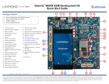
Open-Q™ 410 Development Kit
User Guide
Part Number PMD-0058
Revision A August 2020

Open-Q 410 Dev Kit User Guide 2
Your use of this document is subject to and governed by those terms and conditions in the
LICENSE AND PURCHASE TERMS AND CONDITIONS FOR INTRINSYC DEVELOPMENT
PLATFORM KITS, which you or the legal entity you represent, as the case may be, accepted and
agreed to when purchasing a Development Kit from Intrinsyc Technologies Corporation
(“Agreement”). You may use this document, which shall be considered part of the defined term
“Documentation” for purposes of the Agreement, solely in support of your permitted use of the
Development Kit under the Agreement. Distribution of this document is strictly prohibited without
the express written permission of Intrinsyc Technologies Corporation and its respective licensors,
which they can withhold, condition or delay in its sole discretion.
Lantronix is a trademark of Lantronix, Inc., registered in the United States and other countries.
Intrinsyc is a trademark of Intrinsyc Technologies Corporation, registered in Canada and other
countries.
Qualcomm® is a trademark of Qualcomm® Incorporated, registered in the United States and
other countries. Other product and brand names used herein may be trademarks or registered
trademarks of their respective owners.
This document contains technical data that may be subject to U.S. and international export, re-
export, or transfer (“export”) laws. Diversion contrary to U.S. and international law is strictly
prohibited.
© 2020 Lantronix, Inc. All rights reserved.
Contacts
Lantronix, Inc.
7535 Irvine Center Drive, Suite 100
Irvine, CA 92618, USA
Toll Free: 800-526-8766
Phone: 949-453-3990
Fax: 949-453-3995
IES Customer Support Portal
https://helpdesk.intrinsyc.com
Lantronix Technical Support
http://www.lantronix.com/support
Sales Offices
For a current list of our domestic and international sales offices, go to the Lantronix web site at
http://www.lantronix.com/about-us/contact/

Open-Q 410 Dev Kit User Guide 3
Revision History
Date
Rev.
Comments
June 2015
1.0
Initial release.
Intrinsyc document number: ICS-01RND1181-UG-001
July 2015
1.1
Updates after review
August 2015
1.2
Updated section 4.7, S501 to OFF
July 2016
1.3
Prepared for public release and updated section 3.3, GPS antenna
reference
June 2017
1.4
Updates for Rev 0200 Carrier Board and BSP release 1.4.2
July 2017
1.5
Added note about SW support for battery charging in section 4.3
August 2020
A
Initial Lantronix document.
Added Lantronix document part number, Lantronix logo, branding,
contact information, and links.
For the latest revision of this product document, please go to: http://tech.intrinsyc.com
.

Open-Q 410 Dev Kit User Guide 4
Contents
1 Introduction 6
1.1 Intended Audience ___________________________________________________ 6
1.2 Applicable Documents ________________________________________________ 6
1.3 Reference Documents ________________________________________________ 6
1.4 Terms and Acronyms _________________________________________________ 7
2 Overview 9
2.1 Development Device Notice ____________________________________________ 9
2.2 Anti-Static Handling Procedures ________________________________________ 9
2.3 Kit Contents ________________________________________________________ 9
2.4 Hardware Identification Labels _________________________________________ 10
2.5 Block Diagram _____________________________________________________ 12
2.6 Feature List _______________________________________________________ 12
2.7 Custom Hardware Configurations ______________________________________ 15
3 Open-Q
TM
410 SOM 16
3.1 Carrier Board Connection _____________________________________________ 18
3.2 Wi-Fi / BT Antenna Connection ________________________________________ 18
3.3 GPS Antenna Connection ____________________________________________ 18
4 Open-Q
TM
410 Carrier Board 19
4.1 Boot Configuration Options ___________________________________________ 19
4.2 Buttons and LEDs __________________________________________________ 20
4.3 Power and Battery Connections ________________________________________ 20
4.4 Debug Serial UART over USB _________________________________________ 21
4.5 MIPI CSI Camera Connectors _________________________________________ 22
4.5.1 Open-Q
TM
Carrier Board Rev 0100 __________________________________ 22
4.5.2 Open-Q
TM
Carrier Board Rev 0200 __________________________________ 24
4.6 Display Connector __________________________________________________ 26
4.7 USB Host / Device Connections ________________________________________ 28
4.8 Micro SD Socket ___________________________________________________ 29
4.9 Sensor Expansion Header ____________________________________________ 30
4.10 JTAG Header ______________________________________________________ 32
4.11 Audio Connectors ___________________________________________________ 33
4.11.1 Audio 3.5mm Jacks _____________________________________________ 33
4.11.2 Speaker Connectors ____________________________________________ 34
4.11.3 Digital Mic Header ______________________________________________ 35
4.12 Other Interfaces ____________________________________________________ 36
4.13 System Auto Boot __________________________________________________ 36

Open-Q 410 Dev Kit User Guide 5
5 Output Display Options 37
5.1 On-Board Display ___________________________________________________ 37
5.2 HDMI Output Adapter ________________________________________________ 38
List of Figures
Figure 1 – Assembled Open-Q 410 Development Kit .................................................................... 10
Figure 2 – Open-Q™ 410 Development Kit Block Diagram (Rev 0100 shown here) .................... 12
Figure 3 – Top View of Open-Q 410 SOM ..................................................................................... 16
Figure 4 – Bottom View of Open-Q 410 SOM ............................................................................... 16
Figure 5 – Open-Q™ 410 (APQ8016E) SOM Block Diagram ....................................................... 17
Figure 6 – Buttons, LEDs, and Boot Configuration ........................................................................ 19
Figure 7 – Power Input Jack .......................................................................................................... 20
Figure 8 – Battery Input Header ..................................................................................................... 21
Figure 9 – Debug Serial UART over USB (J401) .......................................................................... 22
Figure 10 – MIPI CSI Camera Connectors on Rev 0100 CB ......................................................... 22
Figure 11 – MIPI CSI Camera Connectors on Rev 0200 CB ......................................................... 24
Figure 12 – Display Connector J801 .............................................................................................. 26
Figure 13 – USB Connections ....................................................................................................... 29
Figure 14 – Micro SD Socket, J901 ............................................................................................... 29
Figure 15 – Sensor Expansion Header .......................................................................................... 30
Figure 16 – JTAG Header .............................................................................................................. 32
Figure 17 – Audio 3.5mm Jacks .................................................................................................... 34
Figure 18 – Speaker Connectors ................................................................................................... 34
Figure 19 – Digital Mic Header ...................................................................................................... 35
Figure 20 – Truly FWVGA Panel ................................................................................................... 37
Figure 21 – HDMI Output Adapter ................................................................................................. 38
List of Tables
Table 1 – Open-Q 410 Development Kit Hardware Features ........................................................ 12
Table 2 – Boot Configuration Options ............................................................................................ 19
Table 3 – Battery Input Header Pinout ........................................................................................... 21
Table 4 – MIPI CSI Camera Connector Pinout (For Rev 0100)..................................................... 23
Table 5 – MIPI CSI Camera Connector Pinout (For Rev 0200)..................................................... 24
Table 6 – Display Connector J801 Pinout...................................................................................... 28
Table 7 – Sensor Expansion Header Pinout .................................................................................. 31
Table 8 – JTAG Header Pinout ...................................................................................................... 32
Table 9 – Audio Path Connections ................................................................................................ 33
Table 10 – Speaker Connector Pinout ........................................................................................... 35
Table 11 – Digital Mic Header Pinout ............................................................................................ 36

Open-Q 410 Dev Kit User Guide 6
1 Introduction
This user guide includes information needed for users to become familiar with the Open-Q™ 410 Development
Kit based on the Qualcomm® APQ8016E processor. The document includes:
• Block Diagrams
• Configuration Options
• System on Module (SOM) hardware features
• Carrier Board hardware features
• Optional Accessories
For background information on the kit, go to: https://www.lantronix.com/products/open-q-410-development-kit/
1.1 Intended Audience
This document is intended for end users who have purchased an Open-Q
TM
410 Development Kit from the
Lantronix web store:
http://shop.intrinsyc.com/collections/qualcomm
1.2 Applicable Documents
Reference
Title
A-1
Intrinsyc Purchase and Software License Agreement for the Open-Q
TM
410
Development Kit
1.3 Reference Documents
Reference
Title
R-1
Open- Q
TM
410 Development Kit Display Board Design Guide Tech Note
R-2
Open- Q
TM
410 Development Kit Camera Board Design Guide Tech Note
R-3
Open- Q
TM
410 Development Kit Carrier Board Design Guide Tech Note
R-4
Open- Q
TM
410 SOM Development Kit HW Revision Guide

1: Introduction
Open-Q 410 Dev Kit User Guide 7
1.4 Terms and Acronyms
Term and acronyms
Definition
AMIC
Analog Microphone
ANC
Audio Noise Cancellation
B2B
Board to Board
BLSP
Bus access manager Low Speed Peripheral;
(Serial interfaces like UART/SPI/I2C/UIM)
BT LE
Bluetooth Low Energy
CB
Carrier Board
CSI
Camera Serial Interface
DP
Display Port
DSI
MIPI Display Serial Interface
EEPROM
Electrically Erasable Programmable Read Only
Memory
eMMC
embedded Multi-Media Card
FCC
US Federal Communications Commission
FWVGA
Full Wide Video Graphics Array
GPS
Global Positioning System
HDMI
High Definition Media Interface
HSIC
High Speed Inter Connect Bus
JTAG
Joint Test Action Group
LNA
Low Noise Amplifier
MIPI
Mobile Industry Processor Interface
MPP
Multi-Purpose Pin
NFC
Near Field Communication
RF
Radio Frequency
SATA
Serial ATA
SLIMBUS
Serial Low-power Inter-chip Media Bus
SMARC
Smart Mobility ARChitecture Specification
- Published by Standardization Group for
Embedded Technologies
SOM
System-On-Module
SPMI
System Power Management Interface
(QUALCOMM PMIC / baseband proprietary
protocol)

1: Introduction
Open-Q 410 Dev Kit User Guide 8
Term and acronyms
Definition
UART
Universal Asynchronous Receiver Transmitter
UIM
User Identity Module
USB
Universal Serial Bus
USB HS
USB High-Speed
USB SS
USB Super-Speed

2: Overview
Open-Q 410 Dev Kit User Guide 9
2 Overview
The Open-Q
TM
410 Development Kit provides an evaluation platform for Qualcomm
TM
APQ8016E processor.
This kit is ideally suited for Android / Linux / Windows Application developers, OEMs, Consumer manufacturers,
Hardware Component Vendors, Video Surveillance, Robotics, etc. to evaluate, optimize, test and deploy
applications that can utilize the Qualcomm APQ8016E series technology.
2.1 Development Device Notice
This development device contains RF/digital hardware and software intended for engineering development,
engineering evaluation, or demonstration purposes only and is intended for use in a controlled environment.
This device is not being placed on the market, leased or sold for use in a residential environment or for use by
the general public as an end user device.
This development device is not intended to meet the requirements of a commercially available consumer device
including those requirements specified in the European Union directives applicable for Radio devices being
placed on the market, FCC equipment authorization rules or other regulations pertaining to consumer devices
being placed on the market for use by the general public.
This development device may only be used in a controlled user environment where operators have obtained
the necessary regulatory approvals for experimentation using a radio device and have appropriate technical
training. The device may not be used by members of the general population or other individuals that have not
been instructed on methods for conducting controlled experiments and taking necessary precautions for
preventing harmful interference and minimizing RF exposure risks. Additional RF exposure information can be
found on the FCC website at:
http://www.fcc.gov/oet/rfsafety/
2.2 Anti-Static Handling Procedures
The Open-Q
TM
410 Development Kit is an open frame PCB assembly with exposed integrated circuits.
Accordingly, proper anti-static precautions should be employed when handling the kit, including:
• Use a grounded anti-static mat
• Use a grounded wrist or foot strap
2.3 Kit Contents
The Open-Q™ 410 Development Kit is shipped with the following (see figure below):
• Open-Q™ 410 SOM with APQ8016E processor
• Android 5.0 (lollipop) pre-loaded
• 13mm x 13mm Carrier Board
• AC power adapter

2: Overview
Open-Q 410 Dev Kit User Guide 10
Figure 1 – Assembled Open-Q 410 Development Kit
There are also some optional accessories available for the Open-Q 410 Development Kit, such as:
• Open-Q™ 5MP (OmniVision OV5640) Camera Module (For Rev 0100)
• Open-Q
TM
13MP (Sony IMX214) Camera Module (For Rev 0200)
• 4.46” FWVGA MIPI DSI LCD with capacitive multi-touch
• 4.5” FWVGA MIPI DSI LCD with capacitive multi-touch
For details on purchasing accessories, go to:
http://shop.intrinsyc.com/collections/dragonboard-accessories
2.4 Hardware Identification Labels
Labels are present on the SOM and Carrier boards that include the following information:
• SOM Serial Number
• SOM Wi-Fi MAC Address
• Carrier Board Serial Number
Users are required to enter their SOM serial number when registering on:
http://helpdesk.intrinsyc.com

2: Overview
Open-Q 410 Dev Kit User Guide 11
NOTE:
Users should retain a copy of the SOM and Carrier Board label information for warranty and support purposes.

2: Overview
Open-Q 410 Dev Kit User Guide 12
2.5 Block Diagram
The block diagram for the Open-Q
TM
410 Development Kit is shown below.
Figure 2 – Open-Q™ 410 Development Kit Block Diagram (Rev 0100 shown here)
2.6 Feature List
The table below lists the features of the Open-Q 410 Development Kit hardware.
Table 1 – Open-Q 410 Development Kit Hardware Features
Subsystem or
Connectors
Feature Set Description Specification
Chipset
APQ8016E Qualcomm
TM
APQ8016E
64-bit Quad 1.2GHz ARM
Cortex-A53 with 512kB L2
cache. Adreno
TM
A306 3D
graphics core.
PM8916
QUALCOMM® companion
PMIC for APQ8016E
processor
Includes audio codec
functionality

2: Overview
Open-Q 410 Dev Kit User Guide 13
Subsystem or
Connectors
Feature Set Description Specification
Memory
1GB LPDDR3 32-bit 533MHz
embedded multi chip
package (eMCP)
8 GB eMMC eMMC4.5 / HS200
embedded multi chip
package (eMCP)
Connectivity
Wi-Fi 2.4Ghz via
WCN3620
QUALCOMM® WCN3620 Wi-
Fi + BT Combo Chip
802.11b/g/n single band
BT 4.0 via
WCN3620
QUALCOMM® WCN3620 Wi-
Fi + BT Combo Chip
BT 4.0 + BLE
GPS receiver QUALCOMM® WGR7640
GPS, GLONASS,
COMPASS
RF Interfaces
1x WLAN / BT
Antenna Connectors
on SOM and 1 PCB
Antennas on Carrier
Board
Internal/External BT / WIFI
Antenna
U.FL connector
1x GPS Antenna
Connectors on SOM
External GPS Antenna
connector
U.FL connector
Audio Headset support
Headset connection with
stereo output, microphone
input and jack detection
3.5mm Modular Jack
Audio input
Stereo line input
3.5mm Modular Jack
Audio output
Loud speaker and earpiece
audio outputs
Digital Mic
Digital microphone input
Buttons
Power Button
Power Button
NA
Volume Up
Increase Volume Button
NA
Volume Down
Decrease Volume button/
Reset
NA
Indicating LED Power ON
Power presence indicator.
Red LED

2: Overview
Open-Q 410 Dev Kit User Guide 14
Subsystem or
Connectors
Feature Set Description Specification
USER LED 1-4
User LEDs
Sensors & IoT
Expansion
Sensor / IoT
Expansion Header
Support for Sensor (optional
ST Micro sensor board)
Support for Lantronix IoT
Development Kit
Interfaces and
Connectors
1 x DC Jack
DC Power Supply
1 x Battery
Development
Reserved to give customer
possibility of battery input
1 x MIPI DSI
60 Pin Display Connector
Optional MIPI based 4.5”
Truly display
4-lane
MIPI Alliance Specification
v1.01
2 x MIPI CSI
Camera Connectors
4-lane and 2-lane
MIPI Alliance Specification
v1.0 compliant
1 x Micro SD card
Slot
4-bit, Dual-Voltage (1.8/2.95
V) up to 200MHz Push-Push
Micro SD Card Slot
Supports XDHC/ SDHC and
SDIO v3.0
1 x HDMI
optional HDMI output
supported via HDMI adapter
board.
HDMI 1.4a, Type A
1 x USB2.0 device
Micro-B USB 2.0 Connector
2 x USB2.0 host
Dual Type-A USB 2.0
Connector
Debug UART
Debug UART via USB Micro-
B connector
FTDI UART to USB Bridge
1 x JTAG
JTAG header

2: Overview
Open-Q 410 Dev Kit User Guide 15
2.7 Custom Hardware Configurations
The Open-Q
TM
410 Development Kit provides is a flexible platform for validating functionality of the ultra-small
26.5mm x 44mm Open-Q
TM
410 SOM that is included with the kit. The small size of the SOM allows for it to be
capable of being designed into a multitude of configurations and custom enclosures. Reference documents R-
1 through R-3 describe how to design custom carrier boards and peripherals for specific applications. For
information on how Lantronix can assist in the development of custom hardware and software designs, go to:
http://helpdesk.intrinsyc.com

3: Open-QTM 410 SOM
Open-Q 410 Dev Kit User Guide 16
3 Open-Q
TM
410 SOM
The Open-Q
TM
410 (APQ8016E) SOM measures 26.5mm x 44mm. A top view of the SOM is shown below.
Figure 3 – Top View of Open-Q 410 SOM
The SOM connects to the Carrier Board with two 100-pin board to board connectors, as shown by the bottom
side view below.
Figure 4 – Bottom View of Open-Q 410 SOM

3: Open-QTM 410 SOM
Open-Q 410 Dev Kit User Guide 17
The block diagram for the SOM is shown below.
2x 100-pin Board to Board Connectors (200 pins total)
SNAPDRAGON 410 (APQ8016)
PM8916
WCN3620
WiFi/BT
LPDDR3
533MHz 1GB
-------------
eMMC4.5
200MHz 8GB
3
V
7
CTRL
POWER OUTPUT
CLK
POWER
SDC1
SDC2
MIPI DSI
0
MIPI CSI0,1
I / Q
WLAN DATA
ANT
USB_HS
JTAG
GPIO
AUDIO
BLOCK OF MUXED PORTS (UP TO 24 GPIO)
(UART
, I
2C, SPI, GPIO), BLSP1-6
AUXILIARY SIGNALS
GPIO,
CLOCKS, CONTROL
BT SSBI
EBI
32-
bit
WGR7640
GPS
I / Q
ANT
SSBI
Figure 5 – Open-Q™ 410 (APQ8016E) SOM Block Diagram
The Open-Q
TM
410 Development Kit is provided with the SOM connected and secured to the Carrier Board.
The sections below include more information for the development kit user.

3: Open-QTM 410 SOM
Open-Q 410 Dev Kit User Guide 18
3.1 Carrier Board Connection
The SOM provides the basic common set of features with minimal integration efforts for end users. This is
achieved with two 100-pin board to board connectors that interface the SOM to the carrier board. The
connectors used are the Samtec ST4 / SS4 family providing a 4mm stack height between the SOM and
carrier board. There are also two mounting holes that allow for an M2.5 screw assembly to be used for
securing the two boards together.
3.2 Wi-Fi / BT Antenna Connection
The SOM includes a U.FL coaxial connector on the top side, which provides the connection to the single band
Wi-Fi / BT antenna feed from the WCN3620. The Open-Q 410 Development Kit is shipped with this antenna
feed connected to a PCB trace antenna on the Carrier board with a U.FL coaxial cable.
The SOM has received Wi-Fi modular regulatory certifications (see FCC ID: 2AFDI-ITCOQ410S
for details).
Please note that the on-board PCB antenna is not the antenna used for the SOM Wi-Fi/BT module
certification.
3.3 GPS Antenna Connection
The SOM includes a U.FL coaxial connector on the top side, which provides the connection to the GPS
antenna feed from the WGR7640. The user can gain access to GPS location data by connecting an external
active antenna to the GPS connector on the SOM. The GPS connector can only supply 1.8V DC, so an
external active antenna that can operate at 1.8V DC is required. A possible GPS antenna to use is the
Taoglas AP.17F.07.0064A. A passive antenna can be used only if the antenna is DC-open. A passive
antenna that has a DC-short will disable GPS function or damage the system. For reference, system is tested
with a passive antenna (Taoglas FXP611.07.0092C) to assure functionality

4: Open-QTM 410 Carrier Board
Open-Q 410 Dev Kit User Guide 19
4 Open-Q
TM
410 Carrier Board
The Open-Q
TM
410 (APQ8016E) Carrier Board measures 13mm x 13mm. See Figure 2 for the carrier board
block diagram.
The sections below provide more information on the Carrier Board feature list listed in section 2. This information
may be useful for development kit users who want to connect other devices or peripherals to the platform. If
there are any discrepancies between this document and the development kit schematics, the latter shall take
precedence.
4.1 Boot Configuration Options
The Open-Q
TM
410 CPU boot mode is selected by two DIP switches found on the carrier board as shown in
the figure below.
Figure 6 – Buttons, LEDs, and Boot Configuration
The user can select the boot mode of the CPU by setting the two DIP switches according to the following
table.
Table 2 – Boot Configuration Options
BOOT OPTIONS
USB BOOT
DIP Switch
BOOT CFG_1
DIP Switch
DEFAULT
USB force boot
ON
X
1. SDC1 (eMMC on SOM)
2. SDC2 (µSDµ socket on Carrier)
3. USB2.0
OFF OFF Default configuration
1. SDC2 (µSDµSD socket on
Carrier)
2. SDC1 (eMMC on SOM)
3. USB2.0
OFF ON

4: Open-QTM 410 Carrier Board
Open-Q 410 Dev Kit User Guide 20
4.2 Buttons and LEDs
There are three buttons on the Carrier Board: Power On/Off, Volume Up and Volume Down. There are also
eight LEDs: Power indicator, User LEDs #1 – 4, WLAN activity, BT activity, and charging status. The positions
of the buttons and LEDs are shown in the figure above.
4.3 Power and Battery Connections
The main power input barrel connector (J201) is located on the top side of Carrier Board, as shown below.
The main power input requires a 10-16VDC supply rated for at least 3A. Lantronix encourages using the
12VDC / 3A power supply provided with the kit. The main power input is protected by a very fast acting 5A
rated fuse. J201 is a center pin positive, 2.5mm barrel jack.
Figure 7 – Power Input Jack
There also exists a 6-pin battery input header on the bottom side of the PCB at J1202, as shown below. If the
user would like to use this header, the following must be done:
• Remove resistors R207 and R209. This will disable the on-board 3.7V buck power supply and allow
the battery header to drive this power rail to the SOM.
• Connect a single cell Lithium battery to J1202 (see pinout details below).
• Remove R1214 in order to enable the linear battery charger on the SOM.
• See figure below for respective resistors and connector location
/