Page is loading ...

Open-Q™ 2100 Development Kit
User Guide
Part Number PMD-00069
Revision A August 2020

Open-Q™ 2100 Dev Kit User Guide 2
Your use of this document is subject to and governed by those terms and conditions in the
LICENSE AND PURCHASE TERMS AND CONDITIONS FOR INTRINSYC DEVELOPMENT
PLATFORM KITS, which you or the legal entity you represent, as the case may be, accepted and
agreed to when purchasing a Development Kit from Intrinsyc Technologies Corporation
(“Agreement”). You may use this document, which shall be considered part of the defined term
“Documentation” for purposes of the Agreement, solely in support of your permitted use of the
Development Kit under the Agreement. Distribution of this document is strictly prohibited without
the express written permission of Intrinsyc Technologies Corporation and its respective licensors,
which they can withhold, condition or delay in its sole discretion.
Lantronix is a trademark of Lantronix, Inc., registered in the United States and other countries.
Intrinsyc is a trademark of Intrinsyc Technologies Corporation, registered in Canada and other
countries.
Qualcomm® is a trademark of Qualcomm® Incorporated, registered in the United States and
other countries. Other product and brand names used herein may be trademarks or registered
trademarks of their respective owners.
This document contains technical data that may be subject to U.S. and international export, re-
export, or transfer (“export”) laws. Diversion contrary to U.S. and international law is strictly
prohibited.
© 2020 Lantronix, Inc. All rights reserved.
Contacts
Lantronix, Inc.
7535 Irvine Center Drive, Suite 100
Irvine, CA 92618, USA
Toll Free: 800-526-8766
Phone: 949-453-3990
Fax: 949-453-3995
IES Customer Support Portal
https://helpdesk.intrinsyc.com
Lantronix Technical Support
http://www.lantronix.com/support
Sales Offices
For a current list of our domestic and international sales offices, go to the Lantronix web site at
http://www.lantronix.com/about-us/contact/

Open-Q™ 2100 Dev Kit User Guide 3
Revision History
Date
Rev.
Comments
April 2017
1.0
Initial release.
Intrinsyc document number: ITC-01RND1260-UG-001
June 2017
1.1
• Fixed wrong RAM/ eMMC size information
• Fixed typo errors on the table 3.9-5 and section 3.8
• Added Getting started section 3.6
• Added section coin cell battery holder FM connector,
micro SD card and Ethernet connector section 3.9.X
• Removed information related to REV 1 SOM and Carrier.
Added REV2 carrier board changes.
October 2017
1.2
Added instructions to change display from HDMI to LCD.
April 2018
1.3
Improved instructions for switching display output
March 2019
1.4
Fixed error in Wi-Fi specification
Updated cover photo
August 2020
A
Initial Lantronix document.
Added Lantronix document part number, Lantronix logo, branding,
contact information, and links.
For the latest revision of this product document, please go to: http://tech.intrinsyc.com
.

Open-Q™ 2100 Dev Kit User Guide 4
Contents
1 Introduction 6
1.1 Purpose ____________________________________________________________ 6
1.2 Scope _____________________________________________________________ 6
1.3 Intended Audience ___________________________________________________ 6
2 Documents 7
2.1 Applicable Documents_________________________________________________ 7
2.2 Reference Documents_________________________________________________ 7
2.3 Terms and Acronyms _________________________________________________ 7
3 Open-Q 2100 Development Kit 11
3.1 Introduction ________________________________________________________ 11
3.2 Development Platform Notice __________________________________________ 11
3.3 Anti-Static Handling Procedures ________________________________________ 11
3.4 Kit Contents ________________________________________________________ 11
3.5 Hardware Identification Label __________________________________________ 12
3.6 Getting Started _____________________________________________________ 12
3.6.1 Default DIP switch settings _________________________________________ 13
3.6.2 Powering up the Open-Q 2100 Development Kit ________________________ 13
3.6.3 Changing Display Output __________________________________________ 14
3.7 System Block Diagram _______________________________________________ 14
3.8 Open-Q 2100 SOM __________________________________________________ 16
3.8.1 SOM Mechanical Properties ________________________________________ 16
3.8.2 SOM Block Diagram ______________________________________________ 16
3.8.3 Hardware Specification ____________________________________________ 17
3.8.4 SOM RF Specification for WIFI, BT, GNSS ____________________________ 19
3.9 Open-Q 2100 SOM Carrier Board _______________________________________ 20
3.9.1 Dip switch S3400 Configuration Options ______________________________ 21
3.9.2 Dip switch S1700 Configuration Options ______________________________ 22
3.9.3 Carrier Board Expansion Connectors _________________________________ 23
3.9.4 DC Power Input J3000 ____________________________________________ 26
3.9.5 Battery Header J3200 _____________________________________________ 27
3.9.6 Debug Serial UART over USB J2700 _________________________________ 28
3.9.7 Sensor IO Expansion Header J2600 _________________________________ 29
3.9.8 Digital IO (Low Speed) expansion header J2601 ________________________ 31
3.9.9 Audio IO Expansion (PMIC) Header J3600 ____________________________ 32
3.9.10 Headset jack J3702 _____________________________________________ 33
3.9.11 On Board PCB mount WLAN Antenna _______________________________ 33
3.9.12 Open-Q 2100 Display ____________________________________________ 34
3.9.13 HDMI Connector J2400 __________________________________________ 35

Open-Q™ 2100 Dev Kit User Guide 5
3.9.14 Display Connector J2300 _________________________________________ 35
3.9.15 Camera Connector J2500 _________________________________________ 39
3.9.16 USB 2.0 Client Port J2800 ________________________________________ 42
3.9.17 USB 2.0 host interface ___________________________________________ 42
3.9.18 Coin cell battery holder ___________________________________________ 43
3.9.19 FM connector J1801 _____________________________________________ 43
3.9.20 Micro-SD card connector J1900 ____________________________________ 43
3.9.21 Ethernet connector J2801 _________________________________________ 44
3.9.22 Power probe J202 _______________________________________________ 44
3.9.23 GNSS external antenna connector J3501 ____________________________ 45

Open-Q™ 2100 Dev Kit User Guide 6
1 Introduction
1.1 Purpose
The purpose of this user guide is to provide primary technical information on the Open-Q™ 2100 Development
Kit based on the Qualcomm™ 2100 (APQ8009W) Processor.
For more background information on this development kit, visit:
https://www.lantronix.com/products/open-q-
2100-development-kit/
1.2 Scope
This document will cover the following items on the Open-Q 2100 Development Kit:
• Block Diagram and Overview
• Hardware Features
• Configuration
• SOM
• Carrier Board
• Display Board for LCD (Optional)
1.3 Intended Audience
This document is intended for users who would like to develop custom applications on the Open-Q 2100
Development Kit.

Documents
Open-Q™ 2100 Dev Kit User Guide 7
2 Documents
This section lists the supplementary documents for the Open-Q 2100 Development Kit.
2.1 Applicable Documents
Reference
Title
A-1
Intrinsyc Purchase and Software License Agreement for the Open-Q
Development
Kit
2.2 Reference Documents
Reference
Title
R-1
Hardware Document Set for the Qualcomm APQ8009W based on Open-Q
Development Kit
R-2
Open-Q 2100 Schematics (SOM, Carrier)
2.3 Terms and Acronyms
Term and acronyms
Definition
AMIC
Analog Microphone
ANC
Audio Noise Cancellation
B2B
Board to Board
BLSP
Bus access manager Low Speed Peripheral (Serial
interfaces like UART / SPI / I2C/ UIM)
BT LE
Bluetooth Low Energy
CSI
Camera Serial Interface
DSI
MIPI Display Serial Interface
EEPROM
Electrically Erasable Programmable Read only
memory
eMMC
Embedded Multimedia Card
FCC
US Federal Communications Commission
FWVGA
Full Wide Video Graphics Array

Documents
Open-Q™ 2100 Dev Kit User Guide 8
Term and acronyms
Definition
GPS
Global Positioning system
HDMI
High Definition Media Interface
HSIC
High Speed Inter Connect Bus
JTAG
Joint Test Action Group
LNA
Low Noise Amplifier
MIPI
Mobile Industry processor interface
MPP
Multi-Purpose Pin
NFC
Near Field Communication
RF
Radio Frequency
SATA
Serial ATA
SLIMBUS
Serial Low-power Inter-chip Media Bus
SOM
System On Module
SPMI
System Power Management Interface
(Qualcomm® PMIC / baseband proprietary
protocol)
SSBI
Single wire serial bus interface (Qualcomm®
proprietary mostly PMIC / Companion chip and
baseband processor protocol)
UART
Universal Asynchronous Receiver Transmitter
UIM
User Identity module
USB
Universal Serial Bus
USB HS
USB High Speed

Documents
Open-Q™ 2100 Dev Kit User Guide 9
List of Figures
Figure 1 Open-Q 2100 Development Kit .............................................................................................. 12
Figure 2 Cable connection and DIP switches on the Open-Q 2100 Dev kit ........................................ 13
Figure 3 Open-Q 2100 SOM + Carrier Board Block Diagram .............................................................. 15
Figure 4 Open-Q 2100 SOM ................................................................................................................ 16
Figure 5 SOM Block Diagram ............................................................................................................... 17
Figure 6 Open-Q 2100 SOM Antenna locations ................................................................................... 19
Figure 7 Open-Q 2100 Carrier Board ................................................................................................... 20
Figure 8 S3400 DIP switch ................................................................................................................... 21
Figure 9 S1700 DIP switch ................................................................................................................... 22
Figure 10 J3000 12V DC Power Jack .................................................................................................. 26
Figure 11 TP3301 to measure VPH_PWR ........................................................................................... 27
Figure 12 J3200 Battery Header .......................................................................................................... 27
Figure 13 J2700 Debug UART over USB ............................................................................................. 28
Figure 14 J2600 Sensor Expansion Header ........................................................................................ 29
Figure 15 J2601 Digital IO (low speed) expansion header .................................................................. 31
Figure 16 J3600 Audio IO Expansion Header ...................................................................................... 32
Figure 17 J3702 Audio Line Out Jack .................................................................................................. 33
Figure 18 On Board PCB mount antenna connection .......................................................................... 34
Figure 19 HDMI Type A Connector ...................................................................................................... 35
Figure 20 51-Pin Display Connector .................................................................................................... 35
Figure 21 Display Board ....................................................................................................................... 37
Figure 22 Display Board Default Configuration .................................................................................... 38
Figure 23 J2500 Camera Connector .................................................................................................... 39
Figure 24 J2800 USB2.0 for ADB......................................................................................................... 42
Figure 25 J2900 and J2901 USB2.0 Host Ports .................................................................................. 42
Figure 26 B1300 Coin cell holder ......................................................................................................... 43
Figure 27 J1801 FM antenna connector .............................................................................................. 43
Figure 28 J1900 micro-SD card connector ........................................................................................... 43
Figure 29 J2801 Ethernet connector .................................................................................................... 44
Figure 30 J202 Power probe connector ............................................................................................... 44
Figure 31 J3501 GNSS external antenna connector ........................................................................... 45
List of Tables
Table 3.8-1 Open-Q 2100 SOM Hardware Features ........................................................................... 16
Table 3.8-2 Open-Q 2100 SOM Hardware Features ........................................................................... 17
Table 3.9-1 Open-Q 2100 SOM Carrier Board Mechanical Properties ................................................ 20
Table 3.9-2 Dip Switch HW / SW configuration .................................................................................... 21
Table 3.9-3 Dip Switch HW / SW configuration .................................................................................... 23
Table 3.9-4 Carrier Board Expansion Options and Usage ................................................................... 23
Table 3.9-5 Battery Connector Header J3200 Pin out ......................................................................... 28

Documents
Open-Q™ 2100 Dev Kit User Guide 10
Table 3.9-6 Sensor Expansion Header J2600 Pin out ......................................................................... 29
Table 3.9-7 Digital IO (low speed) Expansion Header J2601 Pin out .................................................. 31
Table 3.9-8 Audio IO Expansion (PMIC) Header J3600 Pin out .......................................................... 32
Table 3.9-9 MIPI CSI Camera Connector J2500 Pin out ..................................................................... 39
Table 3.9-10 Power probe J202 Pin out ............................................................................................... 44
Table 3.9-11 DIP switch S3500 configurations .................................................................................... 45

Open-Q 2100 Development Kit
Open-Q™ 2100 Dev Kit User Guide 11
3 Open-Q 2100 Development Kit
3.1 Introduction
The Open-Q 2100 Development Kit provides a reference platform for Qualcomm’s latest 2100 series -
Qualcomm®
2100 processor. This kit is suited for Android / Linux application developers, OEMs, consumer
manufacturers, hardware component vendors, video surveillance, robotics, camera vendors, and flash chip
vendors to evaluate, optimize, test and deploy applications that can utilize the Qualcomm® 2100 series
technology.
3.2 Development Platform Notice
This development platform contains RF/digital hardware and software intended for engineering development,
engineering evaluation, or demonstration purposes only and is meant for use in a controlled environment. This
device is not being placed on the market, leased or sold for use in a residential environment or for use by the
general public as an end user device.
This development platform is not intended to meet the requirements of a commercially available consumer
device including those requirements specified in the European Union directives applicable for Radio devices
being placed on the market, FCC equipment authorization rules or other regulations pertaining to consumer
devices being placed on the market for use by the general public.
This development platform may only be used in a controlled user environment where operators have obtained
the necessary regulatory approvals for experimentation using a radio device and have appropriate technical
training. The device may not be used by members of the general population or other individuals that have not
been instructed on methods for conducting controlled experiments and taking necessary precautions for
preventing harmful interference and minimizing RF exposure risks. Additional RF exposure information can be
found on the FCC website at http://www.fcc.gov/oet/rfsafety/
3.3 Anti-Static Handling Procedures
The Open-Q 2100 Development Kit has exposed electronics and chipsets. Proper anti-static precautions should
be employed when handling the kit, including but not limited to:
• Using a grounded anti-static mat
• Using a grounded wrist or foot strap.
3.4 Kit Contents
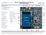
The Open-Q 2100 Development Kit includes the following:
o Open-Q 2100 SOM with the Qualcomm 2100 (APQ8009W) processor, memory, power
management, and WiFi/BT components
o nano-ITX form-factor carrier board
o AC power adapter and HDMI cable
o 4.5” FWVGA (480x854) 16.7 M LCD (Optional Accessory)

Open-Q 2100 Development Kit
Open-Q™ 2100 Dev Kit User Guide 12
Figure 1 Open-Q 2100 Development Kit
The development kit comes with Android for Wearables 7.1.1 software pre-programmed on the CPU board
(SOM). Please contact Lantronix for availability of camera modules, sensor boards, and other accessories:
sales@lantronix.com
3.5 Hardware Identification Label
Labels are present on the CPU board and the nano-ITX form-factor carrier board. The following information is
conveyed on these two boards:
CPU board (SOM):
• Serial Number
• WiFi MAC address
Refer to http://tech.intrinsyc.com/projects/serialnumber/wiki
for more details about locating the serial
number, as this will be needed to register the development kit. To register a development kit, please visit:
https://tech.intrinsyc.com/account/register
Note: Please retain the SOM and carrier board serial number for warranty purposes.
3.6 Getting Started
The instruction in this section explains how to setup the Open-Q 2100 Development Kit.

Open-Q 2100 Development Kit
Open-Q™ 2100 Dev Kit User Guide 13
3.6.1 Default DIP switch settings
The DIP switch S3400 and S1700 is by default set to OFF positions. This setting corresponds to HDMI display
selected, SMB charger enabled, USB forced boot disabled and eMMC boot option selected. See section 3.9.1
and 3.9.2 for other DIP switch settings. Cable connections and DIP switch positions are shown in figure below:
3.6.2 Powering up the Open-Q 2100 Development Kit
To power-up the board, perform the following steps below:
1. At a static-safe workstation, remove the development kit board carefully from the anti-static bag.
2. Connect the HDMI output from the development kit to a display.
3. Connect the Power Adapter to the 12V DC Jack and then press and hold the power button until you
see the Lantronix logo appear on the display (~3 seconds).
4. Plug in a USB mouse to navigate the UI on the HDMI display.
5. If connecting the “Recovery USB” port to a PC for ADB access, make sure to connect this only after the
12V power adapter is connected. Also note that when using the Recovery USB port, the host USB ports
and Ethernet port are disabled.
J3000 (DC IN)
J3200 (Battery
Connector)
J2800, microB USB (recovery/
ADB port)
Figure 2 Cable connection and DIP switches on the Open-Q 2100 Dev kit
WARNING!
The above steps should be followed in exact sequence when battery is not connected to the
Dev Kit. Failing to do so prevents system from booting. If a battery is not connected, the user
has to always plug in the 12V power source before the USB ADB cable is plugged in.

Open-Q 2100 Development Kit
Open-Q™ 2100 Dev Kit User Guide 14
Changing Display Output
The Open-Q 2100 Dev Kit is shipped pre-configured to HDMI display. If you need to change the display output
between LCD and HDMI, use the following commands to switch the display. Note that you also must switch the
HDMI/DSI select DIP switch.
For OSD LCD display
adb reboot bootloader
fastboot oem select-display-panel osd_disp_fwvga_video
fastboot reboot
Switch the HDMI/DSI select switch (S3400-1) to ON to route display signals to the LCD panel. See
section 3.9.1.
For HDMI 720p mode
adb reboot bootloader
fastboot oem select-display-panel adv7533_720p
fastboot reboot
Switch the HDMI/DSI select switch (S3400-1) to OFF to route display signals to the DSI-HDMI bridge
chip. See section 3.9.1.
Please, note that once <fastboot oem> feature is used it will be the only way to switch between HDMI and LCD
modes unless the device is re-flashed.
3.7 System Block Diagram
The Open-Q 2100 SOM development platform consists of three major components
o Open-Q 2100 SOM
o Carrier board for I/O and connecting with external peripherals

Open-Q 2100 Development Kit
Open-Q™ 2100 Dev Kit User Guide 15
o Display Adapter Board (optional accessory)
The following diagram explains the interconnectivity and peripherals on the development kit.
512
MB
LPDDR
3
,
4 GB
eMMC
(PoP)
4-bit SDIO
SOM
Carrier Board
Analog
Audio
Display & Touch
Connector
4L DSI
CSI
Audio
Exp.
Connectors
(PMIC)
DC
Jack
USB
LEDs
BPLSs / GPIOs
Sensor
Connector
SSCs / GPIOs / IRQs
2 x Analog MIC
DSI
Controls
GPIO’s
Low
Speed
Expansion
Header
GPS PCB
antenna
Display Adapter
Coax
5V Buck
SDC2
Touchscreen
SPI
/
I
2
C
HDMI
RST/Vol -
POWER
VOL +
GENERAL
UART
USB
HUB
Type uB
(Recovery
debug/
Charging)
CSI 2Lane
GPIOs/INTs
TTL to
USB
GPIOs
USB Host
Type A
Coin Cell Battery
DSI
4L
DSI to
HDMI
Bridge
HDMI
Type A
Connector
FM
antenna
FM
Antenna
Header
1 x Earphone
1 x Headset
1 x Speaker
User/
Configuration
Switch
USB Host
Type A
Ethernet
Battery
Charger
Battery
Connector
USB HS
VPH_PWR
3.3V
Buck
5V Buck
1.8V
Buck
USB host/client Switch cable detect
DSI Switch Select
Chip Antenna
(2.5/5GHz)
Coax
WiFi
/BT antenna
GNSS antenna
GNSS external
antenna (SMA
connector )
GNSS
front end
Power
sense
USB host VBUS
3.3V
Buck
USB HUB
(USB host/ Ethernet)
5V Boost
HDMI
1.2V
Buck
Camera
APQ8009W
CPU
PM8916
PMIC
WCN3620
WiFi/BT
WGR7640
GNSS
GPS Antenna
switch
headset
connector
Figure 3 Open-Q 2100 SOM + Carrier Board Block Diagram

Open-Q 2100 Development Kit
Open-Q™ 2100 Dev Kit User Guide 16
3.8 Open-Q 2100 SOM
The SOM provides the basic common set of features with minimal integration efforts for end users. It contains
the following:
• Qualcomm™ 2100 Series (APQ8009W) main application processor
• LPDDR3 up to 533MHz 512MB RAM (POP)
• 4GB eMMC flash memory (POP)
• PM8916-1 – PMIC for Peripheral LDOs, Boost Regulators
• WCN3620 Wi-Fi + BT combo chip
• GNSS Receiver (GPS, GLONASS, COMPASS)
Figure 4 Open-Q 2100 SOM
3.8.1 SOM Mechanical Properties
Table 3.8-1 Open-Q 2100 SOM Hardware Features
Dimension
31.5 mm x 15 mm
Interface
2 x 100-pin Hirose DF40 connectors (B2B Connector)
Shielding
A top side shield can for the Wi-Fi/GPS RF section is installed by default.
3.8.2 SOM Block Diagram
The Open-Q 2100 SOM measuring 31.5mm x 15mm is where all the processing occurs. It is connected to the
carrier board via two 100 pin Hirose DF40 connectors. The purpose of these connectors is to bring out essential
signals such that other peripherals can be connected to the platform.
15 mm
31.5 mm
15 mm
31.5 mm

Open-Q 2100 Development Kit
Open-Q™ 2100 Dev Kit User Guide 17
APQ8009W
512
MB
LPDDR3,
4GB
eMMC
(PoP)
PM8916-1
4-bit SDIO
4L DSI
USB HS
WCN
3620
WiFi/BT
GNSS
WGR7640
Open-Q™ 2100
System on Module
IQ + SSBI
CSI 0
JTAG
JTAG
DSI 0
USB
SDC2
RF
RF
Power Circuit
LEDs
RGBMPP
VBAT
UART
Audio
SPMI
2L CSI
GPIO/ MPP
GPIOs
GPIOs
SPI/ I2C
UART
IQ + SSBI
Figure 5 SOM Block Diagram
3.8.3 Hardware Specification
The Open-Q 2100 SOM platform encompasses the following hardware features:
Table 3.8-2 Open-Q 2100 SOM Hardware Features
Subsystem /
Connectors
Feature Set
Description
Specification
Chipset
APQ8009W
Qualcomm® 2100 Processor
ARM Cortex-A7 CPU, quad
core, 32-bit up to 1.09GHz
PMIC (PM8916-1)
Qualcomm® PMIC,
Companion PMIC for
APQ8009W processor
NA
Memory
512MB LPDDR3,
4GB eMMC
Memory POP
Up to 533MHz LPDDR3 POP
on CPU BGA chip. Supports
via 4x32bit channels
Connectivity
Wi-Fi 2.4 GHz via
WCN3620
Wi-Fi Qualcomm WCN3620
Wi-Fi + BT Combo Chip
802.11b/g/n 2.4 GHz via
WCN3620.

Open-Q 2100 Development Kit
Open-Q™ 2100 Dev Kit User Guide 18
Subsystem /
Connectors
Feature Set
Description
Specification
BT 2.4 GHz via
WCN3620
WCN3620
Wi-Fi + BT Combo Chip
Support BT 4.0
GNSS via
WGR7640 – SSBI
Qualcomm®
Proprietary
Protocol
GNS Receiver Frontend
GPS, GLONASS, COMPASS
RF Interfaces
1xWLAN / BT
U.FL antenna
connector
Connect to antenna on
carrier board via coax cable
2.4 GHz WLAN antenna
1x GPS
Connect to external antenna
GPS/GLONASS/COMPASS
passive or active antenna
Interfaces
1 x MIPI CSI
Connect to camera
Connectors
CSI0
MIPI Alliance Specification
v1.0
1 x USB HS
Connect to 2 x dual stack
type A USB2.0 via USB line,
1 x micro USB B 2.0 via
switch (from USB line)
USB2.0
1 x MIPI DSI
Connect to 51- pin display
connector. Interfaces with
Lantronix Display Adapter
Board
MIPI Alliance Specification
v1.01. MIPI D-PHY
Specification v0.65, v0.81,
v0.90, v1.01
Connector
2 x board to board
connector
Connectors to interface with
carrier board
Hirose DF40C series 100pin
connector

Open-Q 2100 Development Kit
Open-Q™ 2100 Dev Kit User Guide 19
3.8.4 SOM RF Specification for WIFI, BT, GNSS
The SOM includes the following radio interfaces:
o Wi-Fi + BT: Antenna 1
o GNSS: Antenna 2
Antenna 1: Antenna 1 is used for providing Wi-Fi and Bluetooth connectivity to WCN3620. This antenna is
meant to be connected to the carrier board via a coaxial cable or to an external antenna. The WCN3620
requires an antenna to be connected here for correct operation.
For details on connecting the Wi-Fi module to the on-board PCB antennas on the carrier board, refer to
section 3.9.11 below.
Antenna 2: Antenna 2 is for the GNSS receiver. This antenna is meant to be connected to the carrier board
via a coaxial cable or to an external antenna. The carrier board includes a GNSS PCB antenna and option to
use an external GNSS antenna via SMA connector. A passive or an active antenna may be used and a 2.7V
bias is provided on the antenna input for powering an active antenna.
The operating frequencies for WGR7640 are:
GPS: 1574.42 MHz – 1576.42 MHz
GLONASS: 1598 MHz to 1606 MHz
Antenna 1
Antenna 2
Figure 6 Open-Q 2100 SOM Antenna locations

Open-Q 2100 Development Kit
Open-Q™ 2100 Dev Kit User Guide 20
3.9 Open-Q 2100 SOM Carrier Board
The Open-Q 2100 SOM Carrier board is a nano-ITX form factor board with various connectors used for
connecting different peripherals. The following are the mechanical properties of the carrier board:
Table 3.9-1 Open-Q 2100 SOM Carrier Board Mechanical Properties
Dimensions
120mm x 120mm
Form Factor
nano-ITX
Major Interfaces
SOM: 2 x 100-pin Hirose DF40 connectors (B2B Connector)
Display: 51 pin JAE (JF08 series) connector
Camera: 41 pin JAE (JF08 series) connector
See section 3.9.3
for details regarding carrier board interfaces
Figure 7 Open-Q 2100 Carrier Board
Debug UART (USB)
Vol (-)
Vol (+)
GP SW
ON/OFF SW
Digital IO
CSI0 Interface
(Camera)
Battery Connector
USB client (recovery/
charging)
DC INPUT (12V)
USB host
USB host
10/100 Ethernet
HDMI
source
W-Fi/ BT
Antenna
DSI0
Interface
(Display)
MicroSD card
slot
Audio (PMIC)
Expansion
SOM connector x2
GNSS PCB
Headset
connector
GPS
external
Antenna
connector
DIP switches
Sensor
/