
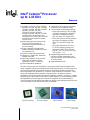
Intel
®
Celeron
®
Processor
up to 1.10 GHz
Datasheet
The Intel
®
Celeron
®
processor is designed for uni-processor based Value PC desktops and is
binary compatible with previous generation Intel architecture processors. The Celeron processor
provides good performance for applications running on advanced operating systems such as
Microsoft* Windows*98, Windows NT*, Windows* 2000, Windows XP* and Linux*. This is
achieved by integrating the best attributes of Intel processors—the dynamic execution
performance of the P6 microarchitecture plus the capabilities of MMX™ technology—bringing
a balanced level of performance to the Value PC market segment. The Celeron processor offers
the dependability you would expect from Intel at an exceptional value. Systems based on
Celeron processors also include the latest features to simplify system management and lower the
cost of ownership for small business and home environments.
■ Available at 1.10 GHz, 1 GHz, 950 MHz,
900 MHz, 850 MHz, 800 MHz, 766 MHz,
733 MHz, 700 MHz, 667 MHz, 633 MHz,
600 MHz, 566 MHz, 533 MHz,
533A MHz, 500 MHz, 466 MHz,
433 MHz, 400 MHz, 366 MHz, 333 MHz,
and 300A MHz core frequencies with
128 KB level-two cache (on die); 300 MHz
and 266 MHz core frequencies without
level-two cache.
■ Intel’s latest Celeron
®
processors in the
FC-PGA/FC-PGA2 package are
manufactured using the advanced 0.18
micron technology.
■ Binary compatible with applications
running on previous members of the Intel
microprocessor line.
■ Dynamic execution microarchitecture.
■ Operates on a 100/66 MHz, transaction-
oriented system bus.
■ Specifically designed for uni-processor
based Value PC systems, with the
capabilities of MMX™ technology.
■ Power Management capabilities.
■ Optimized for 32-bit applications running
on advanced 32-bit operating systems.
■ Uses cost-effective packaging technology.
—Single Edge Processor (S.E.P.) Package
to maintain compatibility with SC242
(processor core frequencies (MHz):
266, 300, 300A, 333, 366, 400, 433).
—Plastic Pin Grid Array (PPGA) Package
(processor core frequencies (MHz):
300A, 333, 366, 400, 433, 466, 500,
533).
—Flip-Chip Pin Grid Array (FC-PGA /
FC-PGA2) Package (processor core
frequencies (MHz); 533A, 566, 600,
633, 667, 700, 733, 766, 800, 850, 900,
950); (GHz); 1, 1.10
■ Integrated high-performance 32 KB
instruction and data, nonblocking, level-
one cache: separate 16 KB instruction and
16 KB data caches.
■ Integrated thermal diode.
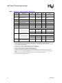
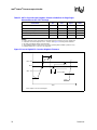
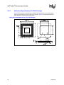
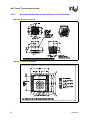
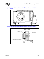
S.E.P. PackageFC-PGA2 Package FC-PGA Package
PPGA Package
Document Number: 243658-020
January 2002

Datasheet
Information in this document is provided in connection with Intel
®
products. No license, express or implied, by estoppel or otherwise, to any intellectual
property rights is granted by this document. Except as provided in Intel’s Terms and Conditions of Sale for such products, Intel assumes no liability
whatsoever, and Intel disclaims any express or implied warranty, relating to sale and/or use of Intel products including liability or warranties relating to
fitness for a particular purpose, merchantability, or infringement of any patent, copyright or other intellectual property right. Intel products are not
intended for use in medical, life saving, or life sustaining applications.
Intel may make changes to specifications and product descriptions at any time, without notice.
Designers must not rely on the absence or characteristics of any features or instructions marked "reserved" or "undefined." Intel reserves these for
future definition and shall have no responsibility whatsoever for conflicts or incompatibilities arising from future changes to them.
The Intel
®
Celeron
®
processor may contain design defects or errors known as errata which may cause the product to deviate from published specifi-
cations. Current characterized errata are available on request.
Contact your local Intel sales office or your distributor to obtain the latest specifications and before placing your product order.
Copies of documents which have an ordering number and are referenced in this document, or other Intel literature, may be obtained by calling
1-800-548-4725 or by visiting Intel’s website at http://www.intel.com.
Intel, Celeron, Pentium, MMX and the Intel logo are trademarks or registered trademarks of Intel Corporation or its subsidiaries in the United States
and other countries.
*Other names and brands may be claimed as the property of others.
Copyright
©
1996–2002, Intel Corporation

Datasheet 3
Intel
®
Celeron
®
Processor up to 1.10 GHz
Contents
1.0 Introduction.......................................................................................................................11
1.1 Terminology.........................................................................................................11
1.1.1 Package Terminology.............................................................................12
1.1.2 Processor Naming Convention...............................................................13
1.2 References..........................................................................................................14
2.0 Electrical Specifications....................................................................................................15
2.1 System Bus and Vref...........................................................................................15
2.2 Clock Control and Low Power States..................................................................15
2.2.1 Normal State—State 1 ...........................................................................16
2.2.2 AutoHALT Power Down State—State 2.................................................16
2.2.3 Stop-Grant State—State 3 .....................................................................17
2.2.4 HALT/Grant Snoop State—State 4 ........................................................17
2.2.5 Sleep State—State 5..............................................................................17
2.2.6 Deep Sleep State—State 6....................................................................18
2.2.7 Clock Control..........................................................................................18
2.3 Power and Ground Pins......................................................................................18
2.3.1 Phase Lock Loop (PLL) Power...............................................................19
2.4 Processor Decoupling.........................................................................................19
2.4.1 System Bus AGTL+ Decoupling.............................................................19
2.5 Voltage Identification...........................................................................................20
2.6 System Bus Unused Pins....................................................................................21
2.7 Processor System Bus Signal Groups................................................................21
2.7.1 Asynchronous Vs. Synchronous for System Bus Signals......................23
2.7.2 System Bus Frequency Select Signal (BSEL[1:0]).................................23
2.8 Test Access Port (TAP) Connection....................................................................23
2.9 Maximum Ratings................................................................................................23
2.10 Processor DC Specifications...............................................................................24
2.11 AGTL+ System Bus Specifications .....................................................................33
2.12 System Bus AC Specifications............................................................................34
3.0 System Bus Signal Simulations........................................................................................52
3.1 System Bus Clock (BCLK) Signal Quality Specifications and
Measurement Guidelines ....................................................................................52
3.2 AGTL+ Signal Quality Specifications and Measurement Guidelines ..................55
3.3 Non-AGTL+ Signal Quality Specifications and Measurement Guidelines...........57
3.3.1 Overshoot/Undershoot Guidelines.........................................................57
3.3.2 Ringback Specification...........................................................................58
3.3.3 Settling Limit Guideline...........................................................................59
3.4 AGTL+ Signal Quality Specifications and Measurement Guidelines
(FC-PGA/FC-PGA2 Packages)...........................................................................59
3.4.1 Overshoot/Undershoot Guidelines (FC-PGA/FC-PGA2 Packages).......59
3.4.2 Overshoot/Undershoot Magnitude (FC-PGA/FC-PGA2 Packages).......59
3.4.3 Overshoot/Undershoot Pulse Duration (FC-PGA/FC-PGA2
Packages) ..............................................................................................60
3.4.4 Activity Factor (FC-PGA/FC-PGA2 Packages) ......................................60

Intel
®
Celeron
®
Processor up to 1.10 GHz
4 Datasheet
3.4.5 Reading Overshoot/Undershoot Specification Tables
(FC-PGA/FC-PGA2 Packages)..............................................................61
3.4.6 Determining if a System meets the Overshoot/Undershoot
Specifications (FC-PGA/FC-PGA2 Packages).......................................62
3.5 Non-AGTL+ Signal Quality Specifications and Measurement Guidelines...........64
4.0 Thermal Specifications and Design Considerations.........................................................65
4.1 Thermal Specifications........................................................................................65
4.1.1 Thermal Diode........................................................................................68
5.0 Mechanical Specifications................................................................................................69
5.1 S.E.P. Package...................................................................................................69
5.1.1 Materials Information..............................................................................69
5.1.2 Signal Listing (S.E.P. Package) ............................................................70
5.2 PPGA Package...................................................................................................79
5.2.1 PPGA Package Materials Information....................................................79
5.2.2 PPGA Package Signal Listing................................................................81
5.3 FC-PGA/FC-PGA2 Packages .............................................................................92
5.3.1 FC-PGA Mechanical Specifications .......................................................92
5.3.2 Mechanical Specifications (FC-PGA2 Package)....................................94
5.3.2.1 Recommended Mechanical Keep-Out Zones
(FC-PGA2 Package) .................................................................96
5.3.3 FC-PGA/FC-PGA2 Package Signal List.................................................97
5.4 Processor Markings (PPGA/FC-PGA/FC-PGA2 Packages).............................108
5.5 Heatsink Volumetric Keepout Zone Guidelines.................................................109
6.0 Boxed Processor Specifications.....................................................................................110
6.1 Mechanical Specifications for the Boxed Intel
®
Celeron
®
Processor................110
6.1.1 Mechanical Specifications for the S.E.P. Package...............................110
6.1.1.1 Boxed Processor Heatsink Weight..........................................112
6.1.1.2 Boxed Processor Retention Mechanism.................................112
6.1.2 Mechanical Specifications for the PPGA Package...............................113
6.1.2.1 Boxed Processor Heatsink Weight..........................................114
6.1.3 Mechanical Specifications for the FC-PGA/FC-PGA2 Packages.........114
6.1.3.1 Boxed Processor Heatsink Weight..........................................115
6.2 Thermal Specifications......................................................................................115
6.2.1 Thermal Requirements for the Boxed Intel
®
Celeron
®
Processor........115
6.2.1.1 Boxed Processor Cooling Requirements ................................115
6.2.1.2 Boxed Processor Thermal Cooling Solution Clip ....................117
6.3 Electrical Requirements for the Boxed Intel
®
Celeron
®
Processor ...................117
6.3.1 Electrical Requirements .......................................................................117
7.0 Processor Signal Description.........................................................................................120
7.1 Signal Summaries.............................................................................................126

Datasheet 5
Intel
®
Celeron
®
Processor up to 1.10 GHz
Figures
1 Clock Control State Machine...............................................................................16
2 BCLK to Core Logic Offset..................................................................................48
3 BCLK*, PICCLK, and TCK Generic Clock Waveform .........................................49
4 System Bus Valid Delay Timings ........................................................................49
5 System Bus Setup and Hold Timings..................................................................49
6 System Bus Reset and Configuration Timings (For the S.E.P. and
PPGA Packages) ................................................................................................50
7 System Bus Reset and Configuration Timings (For the
FC-PGA/FC-PGA2 Package)..............................................................................50
8 Power-On Reset and Configuration Timings.......................................................51
9 Test Timings (TAP Connection)..........................................................................51
10 Test Reset Timings .............................................................................................51
11 BCLK, TCK, PICCLK Generic Clock Waveform at the Processor Core Pins .....53
12 BCLK, TCK, PICCLK Generic Clock Waveform at the Processor
Edge Fingers.......................................................................................................54
13 Low to High AGTL+ Receiver Ringback Tolerance.............................................56
14 Non-AGTL+ Overshoot/Undershoot, Settling Limit, and Ringback .....................57
15 Maximum Acceptable AGTL+ Overshoot/Undershoot Waveform
(FC-PGA/FC-PGA2 Packages)...........................................................................63
16 Non-AGTL+ Overshoot/Undershoot, Settling Limit, and Ringback ....................64
17 Processor Functional Die Layout (CPUID 0686h)...............................................67
18 Processor Functional Die Layout (up to CPUID 0683h)......................................67
19 Processor Substrate Dimensions (S.E.P. Package) ...........................................70
20 Processor Substrate Primary/Secondary Side Dimensions (S.E.P. Package)....70
21 Package Dimensions (PPGA Package)..............................................................79
22 PPGA Package (Pin Side View)..........................................................................81
23 Package Dimensions (FC-PGA Package)...........................................................92
24 Package Dimensions (FC-PGA2 Package).........................................................94
25 Volumetric Keep-Out...........................................................................................96
26 Component Keep-Out .........................................................................................96
27 Package Dimensions (FC-PGA/FC-PGA2 Packages)........................................97
28 Top Side Processor Markings (PPGA Package)...............................................108
29 Top Side Processor Markings (FC-PGA Package)...........................................108
30 Top Side Processor Markings (FC-PGA2 Package) .........................................108
31 Retention Mechanism for the Boxed Intel® Celeron
®
Processor in the
S.E.P. Package.................................................................................................111
32 Side View Space Requirements for the Boxed Processor in the S.E.P.
Package ............................................................................................................111
33 Front View Space Requirements for the Boxed Processor in the S.E.P.
Package ............................................................................................................112
34 Boxed Intel
®
Celeron
®
Processor in the PPGA Package..................................113
35 Side View Space Requirements for the Boxed Processor in the PPGA
Package ............................................................................................................113
36 Conceptual Drawing of the Boxed Intel
®
Celeron
®
Processor in the
370-Pin Socket (FC-PGA/FC-PGA2 Packages)................................................114
37 Dimensions of Mechanical Step Feature in Heatsink Base for the
FC-PGA/FC-PGA2 Packages ...........................................................................114
38 Top View Airspace Requirements for the Boxed Processor in the
S.E.P. Package.................................................................................................115

Intel
®
Celeron
®
Processor up to 1.10 GHz
6 Datasheet
39 Side View Airspace Requirements for the Boxed Intel
®
Celeron
®
Processor in the FC-PGA/FC-PGA2 and PPGA Packages ..............................116
40 Volumetric Keepout Requirements for The Boxed Fan Heatsink......................116
41 Clip Keepout Requirements for the 370-Pin (Top View) ...................................117
42 Boxed Processor Fan Heatsink Power Cable Connector Description ..............118
43 Motherboard Power Header Placement for the S.E.P. Package ......................119
44 Motherboard Power Header Placement Relative to the 370-pin Socket...........119

Datasheet 7
Intel
®
Celeron
®
Processor up to 1.10 GHz
Tables
1 Processor Identification.......................................................................................13
2 Voltage Identification Definition...........................................................................20
3Intel
®
Celeron
®
Processor System Bus Signal Groups.......................................22
4 Absolute Maximum Ratings................................................................................24
5 Voltage and Current Specifications.....................................................................25
6 AGTL+ Signal Groups DC Specifications............................................................31
7 Non-AGTL+ Signal Group DC Specifications......................................................32
8 Processor AGTL+ Bus Specifications .................................................................33
9 System Bus AC Specifications (Clock) at the Processor Edge Fingers
(for S.E.P. Package)............................................................................................35
10 System Bus AC Specifications (Clock) at the Processor
Core Pins (for Both S.E.P. and PGA Packages).................................................36
11 System Bus AC Specifications (SET Clock)........................................................37
12 Valid Intel
®
Celeron
®
Processor System Bus, Core Frequency..........................38
13 System Bus AC Specifications (AGTL+ Signal Group) at the Processor
Edge Fingers (for S.E.P. Package).....................................................................39
14 System Bus AC Specifications (AGTL+ Signal Group) at the Processor
Core Pins (for S.E.P. Package)...........................................................................39
15 Processor System Bus AC Specifications (AGTL+ Signal Group) at the
Processor Core Pins (for PPGA Package)..........................................................40
16 System Bus AC Specifications (AGTL+ Signal Group) at the Processor
Core Pins (for FC-PGA/FC-PGA2 Packages).....................................................40
17 System Bus AC Specifications (CMOS Signal Group) at the Processor
Edge Fingers (for S.E.P. Package).....................................................................41
18 System Bus AC Specifications (CMOS Signal Group) at the Processor
Core Pins (for Both S.E.P., PGA, and FC-PGA/FC-PGA2 Packages)................41
19 System Bus AC Specifications (CMOS Signal Group) .......................................42
20 System Bus AC Specifications (Reset Conditions)
(for Both S.E.P. and PPGA Packages) ...............................................................42
21 System Bus AC Specifications (Reset Conditions) (for the
FC-PGA/FC-PGA2 Packages) ............................................................................42
22 System Bus AC Specifications (APIC Clock and APIC I/O) at the
Processor Edge Fingers (for S.E.P. Package)....................................................43
23 System Bus AC Specifications (APIC Clock and APIC I/O) at the
Processor Core Pins (For S.E.P. and PGA Packages).......................................44
24 System Bus AC Specifications (APIC Clock and APIC I/O)................................45
25 System Bus AC Specifications (TAP Connection) at the Processor
Edge Fingers (For S.E.P. Package)....................................................................45
26 System Bus AC Specifications (TAP Connection) at the Processor
Core Pins (for Both S.E.P. and PPGA Packages)...............................................46
27 System Bus AC Specifications (TAP Connection) ..............................................47
28 BCLK Signal Quality Specifications for Simulation at the Processor Core
(for Both S.E.P. and PPGA Packages) ...............................................................52
29 BCLK/PICCLK Signal Quality Specifications for Simulation at the
Processor Pins (for the FC-PGA/FC-PGA2 Packages).......................................53
30 BCLK Signal Quality Guidelines for Edge Finger Measurement
(for the S.E.P. Package)......................................................................................54
31 AGTL+ Signal Groups Ringback Tolerance Specifications at the
Processor Core (For Both the S.E.P. and PPGA Packages)..............................55

Intel
®
Celeron
®
Processor up to 1.10 GHz
8 Datasheet
32 AGTL+ Signal Groups Ringback Tolerance Specifications at the
Processor Pins (For FC-PGA/FC-PGA2 Packages)...........................................55
33 AGTL+ Signal Groups Ringback Tolerance Guidelines for Edge Finger
Measurement on the S.E.P. Package.................................................................56
34 Signal Ringback Specifications for Non-AGTL+ Signal Simulation at the
Processor Core (S.E.P. and PPGA Packages)...................................................58
35 Signal Ringback Guidelines for Non-AGTL+ Signal Edge Finger
Measurement (S.E.P. Package)..........................................................................58
36 Signal Ringback Specifications for Non-AGTL+ Signal Simulation at the
Processor Pins (FC-PGA/FC-PGA2 Packages)..................................................58
37 Example Platform Information.............................................................................61
38 66 MHz AGTL+ Signal Group Overshoot/Undershoot Tolerance at
Processor Pins (FC-PGA/FC-PGA2 Packages)..................................................62
39 33 MHz CMOS Signal Group Overshoot/Undershoot Tolerance at
Processor Pins (FC-PGA/FC-PGA2 Packages)..................................................63
40 Processor Power for the PPGA and FC-PGA Packages ....................................66
41 Intel
®
Celeron
®
Processor for the FC-PGA2 Package Thermal Design Power .67
42 Thermal Diode Parameters (S.E.P. and PPGA Packages).................................68
43 Thermal Diode Parameters (FC-PGA/FC-PGA2 Packages)...............................68
44 Thermal Diode Interface......................................................................................68
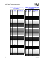
45 S.E.P. Package Signal Listing by Pin Number....................................................71
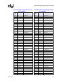
46 S.E.P. Package Signal Listing by Signal Name..................................................75
47 Package Dimensions (PPGA Package)..............................................................80
48 Information Summary (PPGA Package) .............................................................80
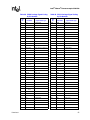
49 PPGA Package Signal Listing by Pin Number....................................................82
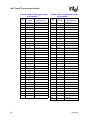
50 PPGA Package Signal Listing in Order by Signal Name ....................................87
51 Package Dimensions (FC-PGA Package) ..........................................................93
52 Processor Die Loading Parameters (FC-PGA Package) ....................................93
53 Package Dimensions (FC-PGA2 Package) ........................................................95
54 Processor Case Loading Parameters (FC-PGA2 Package) ...............................95
55 FC-PGA/FC-PGA2 Signal Listing in Order by Signal Name ...............................98
56 FC-PGA/FC-PGA2 Signal Listing in Order by Pin Number...............................103
57 Boxed Processor Fan Heatsink Spatial Dimensions for the S.E.P. Package ...112
58 Fan Heatsink Power and Signal Specifications.................................................118
59 Alphabetical Signal Reference..........................................................................120
60 Output Signals...................................................................................................126
61 Input Signals .....................................................................................................127
62 Input/Output Signals (Single Driver)..................................................................128
63 Input/Output Signals (Multiple Driver) ...............................................................128

Datasheet 9
Intel
®
Celeron
®
Processor up to 1.10 GHz
Revision History
Revision Date Description
-020 January 2002
• Added IHS specifications for 900 MHz, 950 MHz, and 1 GHz.
• Added 566 MHz specification for CPUID of 068Ah.

Intel
®
Celeron
®
Processor up to 1.10 GHz
10 Datasheet
This page is intentionally left blank.

Datasheet 11
Intel
®
Celeron
®
Processor up to 1.10 GHz
1.0 Introduction
The Intel
®
Celeron
®
processor is based on the P6 microarchitecture and is optimized for the Value
PC market segment. The Intel Celeron processor, like the Pentium
®
II processor, features a
Dynamic Execution microarchitecture and executes MMX™ technology instructions for enhanced
media and communication performance. The Intel Celeron processor also utilizes multiple low-
power states such as AutoHALT, Stop-Grant, Sleep, and Deep Sleep to conserve power during idle
times.
The Intel Celeron processor is capable of running today’s most common PC applications with up to
4 GB of cacheable memory space. As this processor is intended for Value PC systems, it does not
provide multiprocessor support. The Pentium II and Pentium
®
III processors should be used for
multiprocessor system designs.
To be cost-effective at both the processor and system level, the Intel Celeron processor utilizes
cost-effective packaging technologies. They are the S.E.P. (Single-Edge Processor) package, the
PPGA (Plastic Pin Grid Array) package, the FC-PGA (Flip-Chip Pin Grid Array) package, and the
FC-PGA2 (Flip-Chip Pin Grid Array) package. Refer to the Intel
®
Celeron
®
Processor
Specification Update for the latest packaging and frequency support information (Order Number
243337).
Note: This datasheet describes the Intel Celeron processor for the PPGA package, FC-PGA/FC-PGA2
packages, and the S.E.P. Package versions. Unless otherwise specified, the information in this
document applies to all versions and information on PGA packages, refer to both PPGA and
FC-PGA packages.
1.1 Terminology
In this document, a ‘#’ symbol after a signal name refers to an active low signal. This means that a
signal is in the active state (based on the name of the signal) when driven to a low level. For
example, when FLUSH# is low, a flush has been requested. When NMI is high, a nonmaskable
interrupt has occurred. In the case of signals where the name does not imply an active state but
describes part of a binary sequence (such as address or data), the ‘#’ symbol implies that the signal
is inverted. For example, D[3:0] = ‘HLHL’ refers to a hex ‘A’, and D[3:0]# = ‘LHLH’ also refers to
a hex ‘A’ (H= High logic level, L= Low logic level).
The term “system bus” refers to the interface between the processor, system core logic (a.k.a. the
AGPset components), and other bus agents. The system bus is an interface to the processor,
memory, and I/O.

12 Datasheet
Intel
®
Celeron
®
Processor up to 1.10 GHz
1.1.1 Package Terminology
The following terms are used often in this document and are explained here for clarification:
• Processor substrate—The structure on which passive components (resistors and capacitors)
are mounted.
• Processor core—The processor’s execution engine.
• S.E.P. Package—Single-Edge Processor Package, which consists of a processor substrate,
processor core, and passive components. This package differs from the S.E.C. Cartridge as this
processor has no external plastic cover, thermal plate, or latch arms.
• PPGA package—Plastic Pin Grid Array package. The package is a pinned laminated printed
circuit board structure.
• FC-PGA — Flip-Chip Pin Grid Array. The FC-PGA uses the same 370-pin zero insertion
force socket (PGA370) as the PPGA. Thermal solutions are attached directly to the back of the
processor core package without the use of a thermal plate or heat spreader.
• FC-PGA2 — Flip Chip Pin Grid Array 2. The FC-PG2A uses the same 370-pin zero insertion
force socket (PGA370) as the PPGA. The FC-PGA2 package contains an Integrated Heat
Spreader that covers the processor die.
• Keepout zone - The area on or near a FC-PGA/FC-PGA2 packaged processor that system
designs can not utilize.
• Keep-in zone - The area of a FC-PGA packaged processor that thermal solutions may utilize.
Additional terms referred to in this and other related documentation:
• SC242—242-contact slot connector. A processor in the S.E.P. Package uses this connector to
interface with a system board.
• 370-pin socket (PGA370)—The zero insertion force (ZIF) socket in which a processor in the
PPGA package will use to interface with a system board.
• Retention mechanism—A mechanical assembly which holds the package in the SC242
connector.

Datasheet 13
Intel
®
Celeron
®
Processor up to 1.10 GHz
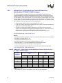
1.1.2 Processor Naming Convention
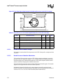
A letter(s) is added to certain processors (e.g., 533A MHz) when the core frequency alone may not
uniquely identify the processor. Below is a summary of what each letter means as well as a table
listing all the FC-PGA/FC-PGA2 processors for the PGA370 socket.
NOTES:
1. Refer to the Intel
®
Celeron
®
Processor Specification Update for the exact CPUID for each processor.
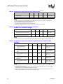
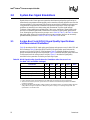
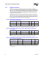
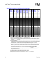
Table 1. Processor Identification
Processor Core Frequency
System Bus Frequency
(MHz)
CPUID
1
300 MHz 300 MHz 66 065xh
300A MHz 300 MHz 66 066xh
366 MHz 366 MHz 66 066xh
400 MHz 400 MHz 66 066xh
433 MHz 433 MHz 66 066xh
466 MHz 466 MHz 66 066xh
500 MHz 500 MHz 66 066xh
533 MHz 533 MHz 66 066xh
533A MHz 533 MHz 66 068xh
566 MHz 566 MHz 66 068xh
600 MHz 600 MHz 66 068xh
633 MHz 633 MHz 66 068xh
667 MHz 667 MHz 66 068xh
700 MHz 700 MHz 66 068xh
733 MHz 733 MHz 66 068xh
766 MHz 766 MHz 66 068xh
800 MHz 800 MHz 100 068xh
850 MHz 850 MHz 100 068xh
900 MHz 900 MHz 100 068xh
950 MHz 950 MHz 100 068xh
1 GHz 1 GHz 100 068xh
1.10 GHz 1.10 MHz 100 068xh

14 Datasheet
Intel
®
Celeron
®
Processor up to 1.10 GHz
1.2 References
The reader of this specification should also be familiar with material and concepts presented in the
following documents:
• AP-485, Intel
®
Processor Identification and the CPUID Instruction (Order Number 241618)
1
• AP-589, Design for EMI (Order Number 243334)
1
• AP-900, Identifying Support for Streaming SIMD Extensions in the Processor and Operating
System
1
• AP-905, Pentium
®
III Processor Thermal Design Guidelines
1
• AP-907, Pentium
®
III Processor Power Distribution Guidelines
1
• Intel
®
Pentium
®
III Processor for the PGA370 Socket at 500 MHz to 933 MHz Datasheet
(Order Number 245264)
• Intel
®
Pentium
®
III Processor Thermal Metrology for CPUID 068h Family
1
• Intel
®
Pentium
®
III Processor Software Application Development Application Notes
1
• Intel
®
Celeron
®
Processor Specification Update (Order Number 243748)
• 370-Pin Socket (PGA370) Design Guidelines (Order Number 244410)
• Intel
®
Architecture Software Developer's Manual (Order Number 243193)
— Volume I: Basic Architecture (Order Number 243190)
— Volume II: Instruction Set Reference (Order Number 243191)
— Volume III: System Programming Guide (Order Number 243192)
• Intel
®
440EX AGPset Design Guide (Order Number 290637)
• Intel
®
Celeron
®
Processor with the Intel
®
440LX AGPset Design Guide
(Order Number 245088)
• Intel
®
440BX AGPset Design Guide (Order Number 290634)
• Intel
®
Celeron
®
Processor with the Intel
®
440ZX-66 AGPset Design Guide
(Order Number 245126)
• Intel
®
Celeron
®
Processor (PPGA) at 466 MHz Thermal Solutions Guidelines
(Order Number 245156)
Notes:
1. This reference material can be found on the Intel Developer’s Web site located at
http://developer.intel.com.
2. For a complete listing of the Intel
®
Celeron
®
processor reference material, refer to the Intel
Developer’s Web site when this processor is formally launched. The Web site is located at
http://developer.intel.com/design/celeron/.

Datasheet 15
Intel
®
Celeron
®
Processor up to 1.10 GHz
2.0 Electrical Specifications
2.1 System Bus and VREF
Celeron processor signals use a variation of the low voltage Gunning Transceiver Logic (GTL)
signaling technology. The Intel
Celeron processor system bus specification is similar to the GTL
specification, but has been enhanced to provide larger noise margins and reduced ringing. The
improvements are accomplished by increasing the termination voltage level and controlling the
edge rates. Because this specification is different from the standard GTL specification, it is referred
to as Assisted Gunning Transceiver Logic (AGTL+) in this document.
The Celeron processor varies from the Pentium Pro processor in its output buffer implementation.
The buffers that drive the system bus signals on the Celeron processor are actively driven to
V
CC
CORE
for one clock cycle during the low-to-high transition. This improves rise times and
reduces overshoot. These signals should still be considered open-drain and require termination to a
supply that provides the logic-high signal level.
The AGTL+ inputs use differential receivers which require a reference signal (V
REF). VREF is used
by the receivers to determine if a signal is a logic-high or a logic-low, and is provided to the
processor core by either the processor substrate (S.E.P. Package) or the motherboard (PGA370
socket). Local V
REF copies should be generated on the motherboard for all other devices on the
AGTL+ system bus.
Termination is used to pull the bus up to the high voltage level and to control reflections on the
transmission line. The processor may contain termination resistors (S.E.P. Package, FC-PGA
Package, and FC-PGA2 Package) that provide termination for one end of the Intel Celeron
processor system bus. Otherwise, this termination must exist on the motherboard.
Solutions exist for single-ended termination as well, though this implementation changes system
design and eliminate backwards compatibility for Celeron processors in the PPGA package.
Single-ended termination designs must still provide an AGTL+ termination resistor on the
motherboard for the RESET# signal.
The AGTL+ bus depends on incident wave switching. Therefore timing calculations for AGTL+
signals are based on motherboard flight time as opposed to capacitive deratings. Analog signal
simulation of the Intel Celeron processor system bus, including trace lengths, is highly
recommended when designing a system. See the Pentium
®
II Processor AGTL+ Layout Guidelines
and the Pentium
®
II Processor I/O Buffer Models, Quad Format (Electronic Form) for details.
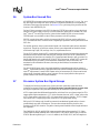
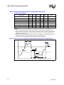
2.2 Clock Control and Low Power States
Celeron processors allow the use of AutoHALT, Stop-Grant, Sleep, and Deep Sleep states to reduce
power consumption by stopping the clock to internal sections of the processor, depending on each
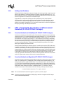
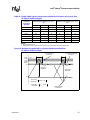
particular state. See Figure 1 for a visual representation of the Intel Celeron processor low power
states.
For the processor to fully realize the low current consumption of the Stop-Grant, Sleep, and Deep
Sleep states, a Model Specific Register (MSR) bit must be set. For the MSR at 02Ah (hex), bit 26
must be set to a ‘1’ (this is the power on default setting) for the processor to stop all internal clocks
during these modes. For more information, see the Pentium
®
II Processor Developer's Manual
(Order Number 243502).

16 Datasheet
Intel
®
Celeron
®
Processor up to 1.10 GHz
2.2.1 Normal State—State 1
This is the normal operating state for the processor.
2.2.2 AutoHALT Power Down State—State 2
AutoHALT is a low power state entered when the processor executes the HALT instruction. The
processor will transition to the Normal state upon the occurrence of SMI#, BINIT#, INIT#, or
LINT[1:0] (NMI, INTR). RESET# will cause the processor to immediately initialize itself.
The return from a System Management Interrupt (SMI) handler can be to either Normal Mode or
the AutoHALT Power Down state. See the Intel Architecture Software Developer's Manual,
Volume III: System Programmer's Guide (Order Number 243192) for more information.
FLUSH# will be serviced during the AutoHALT state, and the processor will return to the
AutoHALT state.
The system can generate a STPCLK# while the processor is in the AutoHALT Power Down state.
When the system deasserts the STPCLK# interrupt, the processor will return execution to the
HALT state.
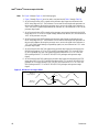
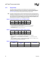
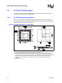
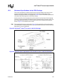
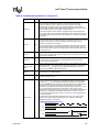
Figure 1. Clock Control State Machine
2. Auto HALT Power Down State
BCLK running.
Snoops and interrupts allowed.
4. Auto HALT Power Down State
BCLK running.
Snoops and interrupts allowed.
Snoop
Event
Occurs
Snoop
Event
Serviced
HALT Instruction and
HALT Bus Cycle generated
INIT#, BINIT#, INTR, SMI#,
RESET#
Snoop event occurs
Snoop event serviced
1. Normal State
Normal execution.
3. Stop Grant State
BCLK running.
Snoops and interrupts allowed.
STPCLK#
asserted
STPCLK#
deasserted
5. Sleep State
BCLK running.
Snoops and interrupts allowed.
SLP#
asserted
SLP#
deasserted
6. Deep Sleep State
BCLK stopped.
No Snoops and interrupts allowed.
BCLK
input
stopped
BCLK
input
restarted
STPCLK# Deasserted
and Stop Grant entered
from Auto HALT.

Datasheet 17
Intel
®
Celeron
®
Processor up to 1.10 GHz
2.2.3 Stop-Grant State—State 3
The Stop-Grant state on the processor is entered when the STPCLK# signal is asserted.
Since the AGTL+ signal pins receive power from the system bus, these pins should not be driven
(allowing the level to return to V
TT) for minimum power drawn by the termination resistors in this
state. In addition, all other input pins on the system bus should be driven to the inactive state.
BINIT# will not be serviced while the processor is in Stop-Grant state. The event will be latched
and can be serviced by software upon exit from Stop-Grant state.
FLUSH# will not be serviced during Stop-Grant state.
RESET# will cause the processor to immediately initialize itself, but the processor will stay in
Stop-Grant state. A transition back to the Normal state will occur with the deassertion of the
STPCLK# signal.
A transition to the HALT/Grant Snoop state will occur when the processor detects a snoop on the
system bus (see Section 2.2.4). A transition to the Sleep state (see Section 2.2.5) will occur with the
assertion of the SLP# signal.
While in the Stop-Grant State, SMI#, INIT#, and LINT[1:0] will be latched by the processor, and
only serviced when the processor returns to the Normal State. Only one occurrence of each event
will be recognized upon return to the Normal state.
2.2.4 HALT/Grant Snoop State—State 4
The processor will respond to snoop transactions on the Celeron processor system bus while in
Stop-Grant state or in AutoHALT Power Down state. During a snoop transaction, the processor
enters the HALT/Grant Snoop state. The processor will stay in this state until the snoop on the Intel
Celeron processor system bus has been serviced (whether by the processor or another agent on the
Intel Celeron processor system bus). After the snoop is serviced, the processor will return to the
Stop-Grant state or AutoHALT Power Down state, as appropriate.
2.2.5 Sleep State—State 5
The Sleep state is a very low power state in which the processor maintains its context, maintains
the phase-locked loop (PLL), and has stopped all internal clocks. The Sleep state can only be
entered from Stop-Grant state. Once in the Stop-Grant state, the SLP# pin can be asserted, causing
the processor to enter the Sleep state. The SLP# pin is not recognized in the Normal or AutoHALT
states.
Snoop events that occur while in Sleep State or during a transition into or out of Sleep state will
cause unpredictable behavior.
In the Sleep state, the processor is incapable of responding to snoop transactions or latching
interrupt signals. No transitions or assertions of signals (with the exception of SLP# or RESET#)
are allowed on the system bus while the processor is in Sleep state. Any transition on an input
signal before the processor has returned to Stop-Grant state will result in unpredictable behavior.
If RESET# is driven active while the processor is in the Sleep state, and held active as specified in
the RESET# pin specification, then the processor will reset itself, ignoring the transition through
Stop-Grant State. If RESET# is driven active while the processor is in the Sleep State, the SLP#
and STPCLK# signals should be deasserted immediately after RESET# is asserted to ensure the
processor correctly executes the Reset sequence.

18 Datasheet
Intel
®
Celeron
®
Processor up to 1.10 GHz
While in the Sleep state, the processor is capable of entering its lowest power state, the Deep Sleep
state, by stopping the BCLK input. (See Section 2.2.6.) Once in the Sleep state, the SLP# pin can
be deasserted if another asynchronous system bus event occurs. The SLP# pin has a minimum
assertion of one BCLK period.
2.2.6 Deep Sleep State—State 6
The Deep Sleep state is the lowest power state the processor can enter while maintaining context.
The Deep Sleep state is entered by stopping the BCLK input (after the Sleep state was entered from
the assertion of the SLP# pin). The processor is in Deep Sleep state immediately after BLCK is
stopped. It is recommended that the BLCK input be held low during the Deep Sleep State. Stopping
of the BCLK input lowers the overall current consumption to leakage levels.
To re-enter the Sleep state, the BCLK input must be restarted. A period of 1 ms (to allow for PLL
stabilization) must occur before the processor can be considered to be in the Sleep State. Once in
the Sleep state, the SLP# pin can be deasserted to re-enter the Stop-Grant state.
While in Deep Sleep state, the processor is incapable of responding to snoop transactions or
latching interrupt signals. No transitions or assertions of signals are allowed on the system bus
while the processor is in Deep Sleep state. Any transition on an input signal before the processor
has returned to Stop-Grant state will result in unpredictable behavior.
2.2.7 Clock Control
BCLK provides the clock signal for the processor and on die L2 cache. During AutoHALT Power
Down and Stop-Grant states, the processor processes a system bus snoop. The processor does not
stop the clock to the L2 cache during AutoHALT Power Down or Stop-Grant states. Entrance into
the Halt/Grant Snoop state allows the L2 cache to be snooped, similar to the Normal state.
When the processor is in the Sleep or Deep Sleep states, it does not respond to interrupts or snoop
transactions. During the Sleep state, the internal clock to the L2 cache is not stopped. During the
Deep Sleep state, the internal clock to the L2 cache is stopped. The internal clock to the L2 cache
will be restarted only after the internal clocking mechanism for the processor is stable (i.e., the
processor has re-entered Sleep state).
PICCLK should not be removed during the AutoHALT Power Down or Stop-Grant states.
PICCLK can be removed during the Sleep or Deep Sleep states. When transitioning from the Deep
Sleep state to the Sleep state, PICCLK must be restarted with BCLK.
2.3 Power and Ground Pins
There are five pins defined on the S.E.P. Package for voltage identification (VID) and four pins on
the PPGA, FC-PGA, and FC-PGA2 packages. These pins specify the voltage required by the
processor core. These have been added to cleanly support voltage specification variations on
current and future Celeron processors.
For clean on-chip power distribution, Intel Celeron processors in the S.E.P. Package have 27 V
CC
(power) and 30 V
SS (ground) inputs. The 27 VCC pins are further divided to provide the different
voltage levels to the components. V
CC
CORE
inputs for the processor core account for 19 of the VCC
pins, while 4 V
TT inputs (1.5 V) are used to provide a AGTL+ termination voltage to the processor.
For only the S.E.P. Package, one V
CC
5
pin is provided for Voltage Transient Tools. VCC
5
and
V
CC
CORE
must remain electrically separated from each other.

Datasheet 19
Intel
®
Celeron
®
Processor up to 1.10 GHz
The PPGA package has more power (88) and ground (80) pins than the S.E.P. Package. Of the
power pins, 77 are used for the processor core (V
CC
CORE
) and 8 are used as a AGTL+ reference
voltage (V
REF). The other 3 power pins are VCC
1.5
, VCC
2.5
and VCC
CMOS
and are used for future
processor compatibility.
FC-PGA/FC-PGA2 packages have 77 V
CC
CORE
, 77 ground pins, eight VREF, one VCC
1.5
, one
V
CC
2.5
, and one VCC
CMOS
. VCC
CORE
inputs supply the processor core, including the on-die L2
cache. The V
REF inputs are used as the AGTL+ reference voltage for the processor.
The V
CC
CMOS
pin is provided as a feature for future processor support in a flexible design. In such
a design, the V
CC
CMOS
pin is used to provide the CMOS voltage for use by the platform.
Additionally, 2.5 V must be provided to the V
CC
2.5
input and 1.5 V must be provided to the Vcc
1.5
input. The processor routes the CMOS voltage level through the package that it is compatible with.
For example, processors requiring 1.5 V CMOS voltage levels route 1.5 V to the V
CC
CMOS
output.
Each power signal, regardless of package, must meet the specifications stated in Table 4. In
addition, all V
CC
CORE
pins must be connected to a voltage island while all VSS pins have to
connect to a system ground plane. In addition, the motherboard must implement the V
TT pins as a
voltage island or large trace. Similarly, all V
SS pins must be connected to a system ground plane.
2.3.1 Phase Lock Loop (PLL) Power
It is highly critical that phase lock loop power delivery to the processor meets Intel’s requirements.
A low pass filter is required for power delivery to pins PLL1 and PLL2. This serves as an isolated,
decoupled power source for the internal PLL.
2.4 Processor Decoupling
Due to the large number of transistors and high internal clock speeds, the processor is capable of
generating large average current swings between low and full power states. This causes voltages on
power planes to sag below their nominal values if bulk decoupling is not adequate. Care must be
taken in the board design to ensure that the voltage provided to the processor remains within the
specifications listed in Table 5. Failure to do so can result in timing violations or a reduced lifetime
of the component.
2.4.1 System Bus AGTL+ Decoupling
The S.E.P. Package and FC-PGA/FC-PGA2 packages contain high frequency decoupling
capacitance on the processor substrate, where the PPGA package does not. Therefore, Celeron
processors in the PGA packages require high frequency decoupling on the system motherboard.
Bulk decoupling must be provided on the motherboard for proper AGTL+ bus operation for all
packages. See AP-585, Pentium
®
II Processor AGTL+ Guidelines (Order Number 243330), AP-
587, Pentium
®
II Processor Power Distribution Guidelines (Order Number 243332), and the
Pentium
®
II Processor Developer's Manual (Order Number 243502) for more information.

20 Datasheet
Intel
®
Celeron
®
Processor up to 1.10 GHz
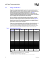
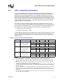
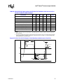
2.5 Voltage Identification
The processor’s voltage identification (VID) pins can be used to automatically select the VCC
CORE
voltage from a compatible voltage regulator. There are five VID pins (VID[4:0]) on the S.E.P.
Package, while there are only four (VID[3:0]) on the PGA packages. This is because there are no
Celeron processors in the PGA package that require more than 2.05 V (see Table 2).
VID pins are not signals, but rather are an open or short circuit to V
SS on the processor. The
combination of opens and shorts defines the processor core’s required voltage. The VID pins also
allow for compatibility with current and future Intel Celeron processors.
Note that the ‘11111’ (all opens) ID can be used to detect the absence of a processor core in a given
slot (S.E.P. Package only), as long as the power supply used does not affect the VID signals.
Detection logic and pull-ups should not affect VID inputs at the power source (see Section 7.0).
External logic monitoring the VID signals or the voltage regulator may require the VID pins to be
pulled-up. If this is the case, the VID pins should be pulled up to a TTL-compatible level with
external resistors to the power source of the regulator.
The power source chosen must be guaranteed to be stable whenever the voltage regulator’s supply
is stable. This will prevent the possibility of the processor supply going above the specified
V
CC
CORE
in the event of a failure in the supply for the VID lines. In the case of a DC-to-DC
converter, this can be accomplished by using the input voltage to the converter for the VID line
pull-ups. In addition, the power supply must supply the requested voltage or disable itself.
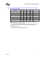
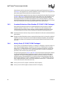
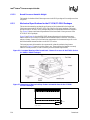
NOTES:
1. 0 = Processor pin connected to V
SS.
2. 1 = Open on processor; may be pulled up to TTL V
IH
on motherboard.
3. The Celeron processor core uses a 2.0 V power source.
4. VID4 applies only to the S.E.P. Package. VID[3:0] applies to both S.E.P. and PGA packages.
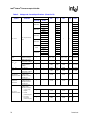
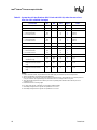
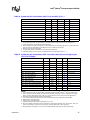
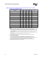
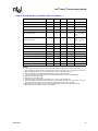
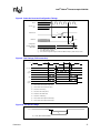
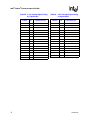
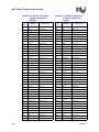
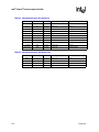
Table 2. Voltage Identification Definition
VID4
(S.E.P.P. only)
VID3 VID2 VID1 VID0 V
CC
CORE
011111.30
011101.35
011011.40
011001.45
010111.50
010101.55
010011.60
010001.65
001111.70
001101.75
001011.80
001001.85
000111.90
000101.95
000012.00
000002.05
11111No Core
4
11110 2.1
4
Page is loading ...
Page is loading ...
Page is loading ...
Page is loading ...
Page is loading ...
Page is loading ...
Page is loading ...
Page is loading ...
Page is loading ...
Page is loading ...
Page is loading ...
Page is loading ...
Page is loading ...
Page is loading ...
Page is loading ...
Page is loading ...
Page is loading ...
Page is loading ...
Page is loading ...
Page is loading ...
Page is loading ...
Page is loading ...
Page is loading ...
Page is loading ...
Page is loading ...
Page is loading ...
Page is loading ...
Page is loading ...
Page is loading ...
Page is loading ...
Page is loading ...
Page is loading ...
Page is loading ...
Page is loading ...
Page is loading ...
Page is loading ...
Page is loading ...
Page is loading ...
Page is loading ...
Page is loading ...
Page is loading ...
Page is loading ...
Page is loading ...
Page is loading ...
Page is loading ...
Page is loading ...
Page is loading ...
Page is loading ...
Page is loading ...
Page is loading ...
Page is loading ...
Page is loading ...
Page is loading ...
Page is loading ...
Page is loading ...
Page is loading ...
Page is loading ...
Page is loading ...
Page is loading ...
Page is loading ...
Page is loading ...
Page is loading ...
Page is loading ...
Page is loading ...
Page is loading ...
Page is loading ...
Page is loading ...
Page is loading ...
Page is loading ...
Page is loading ...
Page is loading ...
Page is loading ...
Page is loading ...
Page is loading ...
Page is loading ...
Page is loading ...
Page is loading ...
Page is loading ...
Page is loading ...
Page is loading ...
Page is loading ...
Page is loading ...
Page is loading ...
Page is loading ...
Page is loading ...
Page is loading ...
Page is loading ...
Page is loading ...
Page is loading ...
Page is loading ...
Page is loading ...
Page is loading ...
Page is loading ...
Page is loading ...
Page is loading ...
Page is loading ...
Page is loading ...
Page is loading ...
Page is loading ...
Page is loading ...
Page is loading ...
Page is loading ...
Page is loading ...
Page is loading ...
Page is loading ...
Page is loading ...
Page is loading ...
Page is loading ...
-
 1
1
-
 2
2
-
 3
3
-
 4
4
-
 5
5
-
 6
6
-
 7
7
-
 8
8
-
 9
9
-
 10
10
-
 11
11
-
 12
12
-
 13
13
-
 14
14
-
 15
15
-
 16
16
-
 17
17
-
 18
18
-
 19
19
-
 20
20
-
 21
21
-
 22
22
-
 23
23
-
 24
24
-
 25
25
-
 26
26
-
 27
27
-
 28
28
-
 29
29
-
 30
30
-
 31
31
-
 32
32
-
 33
33
-
 34
34
-
 35
35
-
 36
36
-
 37
37
-
 38
38
-
 39
39
-
 40
40
-
 41
41
-
 42
42
-
 43
43
-
 44
44
-
 45
45
-
 46
46
-
 47
47
-
 48
48
-
 49
49
-
 50
50
-
 51
51
-
 52
52
-
 53
53
-
 54
54
-
 55
55
-
 56
56
-
 57
57
-
 58
58
-
 59
59
-
 60
60
-
 61
61
-
 62
62
-
 63
63
-
 64
64
-
 65
65
-
 66
66
-
 67
67
-
 68
68
-
 69
69
-
 70
70
-
 71
71
-
 72
72
-
 73
73
-
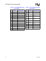 74
74
-
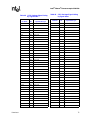 75
75
-
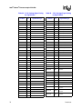 76
76
-
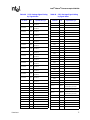 77
77
-
 78
78
-
 79
79
-
 80
80
-
 81
81
-
 82
82
-
 83
83
-
 84
84
-
 85
85
-
 86
86
-
 87
87
-
 88
88
-
 89
89
-
 90
90
-
 91
91
-
 92
92
-
 93
93
-
 94
94
-
 95
95
-
 96
96
-
 97
97
-
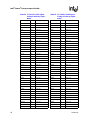 98
98
-
 99
99
-
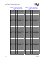 100
100
-
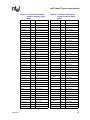 101
101
-
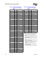 102
102
-
 103
103
-
 104
104
-
 105
105
-
 106
106
-
 107
107
-
 108
108
-
 109
109
-
 110
110
-
 111
111
-
 112
112
-
 113
113
-
 114
114
-
 115
115
-
 116
116
-
 117
117
-
 118
118
-
 119
119
-
 120
120
-
 121
121
-
 122
122
-
 123
123
-
 124
124
-
 125
125
-
 126
126
-
 127
127
-
 128
128


Ask a question and I''ll find the answer in the document
Finding information in a document is now easier with AI
Related papers
-
Intel 200 User manual
-
-
-
-
-
-
-
Intel 830 User manual
-
-
Other documents
-
Protocol 5872-3EC Jet Plane 3D Puzzle User manual
-
Toshiba P4X-0028-512K-533 User manual
-
Supermicro P4X4-028-512K Datasheet
-
Lenovo 59P5107 Datasheet
-
EPOX EP-3C1A User manual
-
 Pinpoint Mounts AM30-BLACK Datasheet
-
Biostar M6VLQ Grand Owner's manual
-
IBM Life Jacket 272 User manual
-
AOpen MX46LS-533V Online Manual
-
