Page is loading ...

User Guide
Please read the sections “Important notice” and “Warnings” at the end of this
document
V 1.0
www.infineon.com/xdp710-001
2023-08-11
UM_2307_PL88_2308_013018
XDP710 evaluation PCBA user guide
Scope and purpose
Setup and evaluation of XP710 printed circuit board assembly (PCBA).
Intended audience
Test engineers.
Table of contents
Table of contents ............................................................................................................................ 1
1 Introduction .......................................................................................................................... 2
2 Hardware and software requirements ...................................................................................... 2
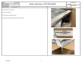
3 XDP710 evaluation platform .................................................................................................... 3
3.1 Electrical specifications .......................................................................................................................... 3
3.2 Block diagram .......................................................................................................................................... 3
3.3 XDP710 evaluation board schematics .................................................................................................... 5
3.4 XDP710 evaluation board layout ............................................................................................................ 7
3.5 XDP710 evaluation board bill of materials ........................................................................................... 12
3.6 XDP710 evaluation board default settings ........................................................................................... 14
3.7 Rsns .......................................................................................................................................................... 16
3.8 FET board ............................................................................................................................................... 16
3.8.1 Different FET footprint options on FET board ...................................................................................... 16
3.9 XDP710 dongle schematics ................................................................................................................... 18
4 Programming, setup, and turn-on instructions ......................................................................... 18
4.1 XDP Designer communication setup .................................................................................................... 19
4.1.1 Check the dongle connection in XDP Designer ............................................................................... 19
4.1.2 Detecting XDP710-002 ...................................................................................................................... 20
4.1.3 Reading and writing registers .......................................................................................................... 22
4.1.4 Program FET ..................................................................................................................................... 23
4.1.5 Program Rsns ...................................................................................................................................... 24
4.1.6 Watchdog timer selection ................................................................................................................ 24
4.1.7 Program current sense range (CS_RNG) and start-up current limit (IST) ...................................... 25
4.1.8 Program VIN_UV_FAULT_LIMIT ....................................................................................................... 25
4.1.9 Program VIN_OV_FAULT_LIMIT ....................................................................................................... 26
4.1.10 Program VOUT_UV_FAULT_LIMIT ................................................................................................... 26
4.2 XDP710 programming under different modes ..................................................................................... 27
4.2.1 FDM ................................................................................................................................................... 27
4.2.1.1 FDM (DCM) ........................................................................................................................................ 27
4.2.1.2 FDM (ACM)......................................................................................................................................... 28
4.2.2 AADM ................................................................................................................................................. 28
5 Loading configuration file ...................................................................................................... 30
6 Hands-on.............................................................................................................................. 32
6.1 Example test: UV fault ........................................................................................................................... 32
6.2 Programming SOA, OTP, and MTP ........................................................................................................ 33
Revision history............................................................................................................................. 35

User Guide
2
V 1.0
2023-08-11
XDP710 evaluation PCBA user guide
Introduction
1 Introduction
Infineon’s XDP700 family (XDP700, XDP710) are highly integrated wide-input voltage system monitoring and
protection devices, which are digitally configurable and use a PMBus communication interface to access their
register map in order to configure all of their features. The XDP710 series dongle is a PC-USB COM port to
PMBus bridge dongle that allows access to the XDP710 registers from the PC software configurator. This
document describes how to set up and use the whole interface for testing purposes, using the Add-Ins menu to
format your document.
2 Hardware and software requirements
The following hardware and software are required for the set-up:
• XDP710 evaluation board V 2.0
• XDP710 USB dongle USB007 or higher
• XDP Designer graphical user interface (GUI)
Figure 1 XDP710 evaluation board
Figure 2 USB007A1 dongle

User Guide
3
V 1.0
2023-08-11
XDP710 evaluation PCBA user guide
XDP710 evaluation platform
Figure 3 XDP Designer GUI
3 XDP710 evaluation platform
The following is a description of the XDP710 evaluation board.
3.1 Electrical specifications
• Input and output voltage range is 12 V DC to 80 V DC.
• The input current range is up to 50 A but can be varied by the number of paralleled MOSFET adapter boards.
The MOSFET adapter boards can be removed and added to the evaluation board based on the required
current level.
3.2 Block diagram
The XDP710 evaluation platform consists of:
• XDP710 evaluation board: Positive input hot-swap controller and e-fuse circuitry designed to run a single
channel controller including its corresponding FET. Communication, control and protection circuitry is also
included.
• USB007A1 dongle: Interface between the computer, which communicates via USB the commands sent by
the XDP Designer GUI, and XDP710, which receives PMBus communication. The USB007A1 dongle translates
from USB to PMBus, as well as enabling the XDP710.
• XDP Designer GUI: Software tool for XDP710 PMBus commands configuration and general control.

User Guide
4
V 1.0
2023-08-11
XDP710 evaluation PCBA user guide
XDP710 evaluation platform
Figure 4 XDP710 evaluation platform block diagram

User Guide
5
V 1.0
2023-08-11
XDP710 evaluation PCBA user guide
XDP710 evaluation platform
3.3 XDP710 evaluation board schematics
Figure 5 Schematic for main IC

User Guide
6
V 1.0
2023-08-11
XDP710 evaluation PCBA user guide
XDP710 evaluation platform
Figure 6 Schematic for main PCBA ports
Figure 7 Schematic for MOSFET PCBA

User Guide
7
V 1.0
2023-08-11
XDP710 evaluation PCBA user guide
XDP710 evaluation platform
3.4 XDP710 evaluation board layout
Figure 8 Top layer layout of main PCB

User Guide
8
V 1.0
2023-08-11
XDP710 evaluation PCBA user guide
XDP710 evaluation platform
Figure 9 Mid 1 layer layout of main PCB

User Guide
9
V 1.0
2023-08-11
XDP710 evaluation PCBA user guide
XDP710 evaluation platform
Figure 10 Mid 2 layer layout of main PCB

User Guide
10
V 1.0
2023-08-11
XDP710 evaluation PCBA user guide
XDP710 evaluation platform
Figure 11 Bottom layer layout of main PCB

User Guide
11
V 1.0
2023-08-11
XDP710 evaluation PCBA user guide
XDP710 evaluation platform
Figure 12 Top, Mid 1, Mid 2 and bottom layer layouts of MOSFET PCB

User Guide
12
V 1.0
2023-08-11
XDP710 evaluation PCBA user guide
XDP710 evaluation platform
3.5 XDP710 evaluation board bill of materials
Table 1 Bill of materials (BOM) for the main PCBA
Item
Qty
Reference
designator
Value
Characteristics
Manufacturer
Part number
1
2
Cin, Ci
0.1 µF
200 V X7R
Murata
GRM31CR72D104K
W03L
2
2
Cout1, Cout2
100 µF
200 V Elect.
Panasonic
EEVEB2D101M
3
1
Cvreg
1 µF
25 V X7R
Murata
GRM188R71E105K
A12
4
2
C1, C9
100 nF
50 V X7R
Murata
GRM188R71H104J
A93
5
1
C2
10 µF
100 V X7S
TDK
C5750X7S2A106M
230KB
6
1
C3
100 nF
100 V X7R
Kemet
C0805X104K1RAC
TU
7
1
C6
3.3 µF
16 V X7R
Murata
GRM21BR71C335K
A99
8
3
C7, C8, C10
1 nF
250 V X7R
Murata
GRM188R72E102K
W07
9
2
D1, D7
Yellowish green
Rohm
Semiconductors
SML-P11MTT86R
10
1
D2
Red
Rohm
Semiconductors
SML-P11UTT86R
11
1
D3
Orange
Rohm
Semiconductors
SML-P11DTT86R
12
1
D4
B3100-13-F
Diodes
Incorporated
B3100-13-F
13
1
D5
5.0SMDJ90A
Bourns
5.0SMDJ90A
14
1
D6
STPS6M100SF
STMicroelectronic
s
STPS6M100SF
15
1
G1
LT3012BEDE#PBF
Analog Devices
LT3012BEDE#PBF
16
2
J1, J2
SO-M5
Würth Elektronik
7466105R
17
4
M1, M2, M3, M4
MTG _Standoff
Keystone
2203
18
4
M5, M6, M7, M8
Screw PHMS 4-40
x 1/4
Keystone
9900
19
2
Q2, Q3
BSR315P
Infineon
BSR315P
20
2
Q4, Q6
2N7002
Infineon
2N7002
21
1
Q5
40 V 0.2 A
Nexperia
MMBT3904,215
22
1
Rin
100
1%
Panasonic
ERJ-8ENF1000V
23
1
Rsns1
N/A
9 W 1%
Bourns
Not used
24
1
Rsns2
0.001
8 W 1%
Bourns
CSS2H-3920R-
1L00F
25
1
Rsns3
N/A
6 W 1%
Bourns
Not used
26
2
R1, R2
1k
1%
Panasonic
ERJ-3EKF1001V
27
2
R3, R7
2k
1%
Panasonic
ERJ-3EKF2001V

User Guide
13
V 1.0
2023-08-11
XDP710 evaluation PCBA user guide
XDP710 evaluation platform
Item
Qty
Reference
designator
Value
Characteristics
Manufacturer
Part number
28
7
R4, R5, R6, R16, R19,
R20, R45
4.7k
1%
Panasonic
ERJ-3EKF4701V
29
1
R8
10
1%
Panasonic
ERJ-3EKF10R0V
30
1
R9
121k
1%
Vishay
CRCW0805121KFK
31
1
R10
4.71k
1%
Yageo
RC0603FR-074K7L
32
12
R11, R12, R13, R35,
R37, R39, R40, R41,
R42, R46, R47, R48
0
1%
Panasonic
ERJ-3GEY0R00V
33
4
R14, R17, R21, R23
12k
1%
Panasonic
ERJ-3EKF1202V
34
4
R15, R18, R22, R24
20k
1%
Panasonic
ERJ-3EKF2002V
35
1
R25
4.53k
1%
Panasonic
ERJ-3EKF4531V
36
1
R26
7.5k
1%
Panasonic
ERJ-3EKF7501V
37
1
R27
11k
1%
Panasonic
ERJ-3EKF1102V
38
1
R28
15k
1%
Panasonic
ERJ-3EKF1502V
39
1
R29
19.6k
1%
Panasonic
ERJ-3EKF1962V
40
1
R30
750k
1%
Panasonic
ERJ-3EKF7503V
41
1
R31
412k
1%
Panasonic
ERJ-3EKF4123V
42
1
R32
24.9k
1%
Panasonic
ERJ-3EKF2492V
43
1
R33
249k
1%
Panasonic
ERJ-3EKF2493V
44
1
R34
147k
1%
Vishay
CRCW0805147KFK
45
1
R36
1.96k
1%
Vishay
CRCW08051K96FK
46
1
R38
2.7k
1%
Vishay
CRCW08052K70FK
47
1
R43
N/A
1%
Not used
48
1
R44
N/A
1%
Not used
49
1
U7
XDP710-002
Infineon
Technologies
XDP710
50
4
XJ23, XJ33, XJ35,
XJ41
CON2_Jumper
Sullins
SPC02SYAN
51
4
X1, X7, X8, X10
Loop
Keystone
5020
52
1
X2
SHF-108-01-L-D-
TH
Samtec
SHF-108-01-L-D-
TH
53
1
X3
Con4
Würth Elektronik
61300411121
54
5
X4, X24, X33, X35, X41
Con2Pin
Harwin
M20-9770246
55
1
X5
M55-7001642R
Harwin
M55-7001642R
56
1
X11
SOC2
AVX
209159002101916
57
1
X13
SMA-J-P-H-ST-
TH1
Samtec
SMA-J-P-H-ST-
TH1
58
2
X14, X23
TSW-103-07-L-S
Samtec
TSW-103-07-L-S
59
2
X15, X18
TSW-106-07-L-D
Samtec
TSW-106-07-L-D
60
1
X21
HTSW-107-07-L-D
Samtec
HTSW-107-07-L-D
61
1
X22
691 210 910 002
Würth Elektronik
6.91211E+11
62
2
X25, X27
Con1Pin-BLK
Würth Elektronik
7464100
63
2
X26, X28
Con1Pin-RED
Würth Elektronik
7464000

User Guide
14
V 1.0
2023-08-11
XDP710 evaluation PCBA user guide
XDP710 evaluation platform
Item
Qty
Reference
designator
Value
Characteristics
Manufacturer
Part number
64
28
X29, X31, X32, X34,
X36, X37, X38, X39,
X42, X43, X46, X47,
X48, X49, X50, X51,
X52, X53, X54, X55,
X56, X57, X58, X59,
X60, X61, X62, X63
SMD loop
Harwin
S2761-46R
Table 2 BOM for MOSFET PCBA
Item
Qty
Reference designator
Value
Voltage
Manufacturer
Part number
1
1
BRD1
PC board
(FAB)
P100147 A
2
1
C4
N/A
X7R
Murata
Not used
3
1
D7
TPSMC100A-
VR
Littelfuse
TPSMC100A-VR
4
1
D8
N/A
Not used
5
1
Q1
N/A
100 V 147 A
Infineon
Not used
6
1
Q6
IPT015N10N5
100 V 300 A
Infineon
IPT015N10N5ATMA1
7
1
Q7
N/A
100 V 300 A
Infineon
Not used
8
1
Q8
N/A
100 V 300 A
Infineon
Not used
9
1
Q9
N/A
100 V 354 A
Infineon
Not used
10
1
R8
10
1%
Panasonic
ERJ-3EKF10R0V
11
1
R45
N/A
1%
Not used
12
1
R46
N/A
1%
Not used
13
1
X8
PLUG2
AVX
109159002101916
14
1
X10
SOCK2
AVX
209159002101916
3.6 XDP710 evaluation board default settings
The jumpers can be found on the board as noted by X15, X18, and X21.
Table 3 Jumper settings:
Reference
designator
Default configuration
Usage
X4
Open
Shorted: Connects FB to voltage divider for over/undervoltage
sensing.
Open: This header can be left open for digital comparator mode
(DCM)
X14
Open
Shorted 1 to 2: Connects UV/EN to VREG
Shorted 2 to 3: Connects UV/EN to GND
Open: UV/EN can be driven by SMA connector or dongle

User Guide
15
V 1.0
2023-08-11
XDP710 evaluation PCBA user guide
XDP710 evaluation platform
X15
Between Pin 5 and 6 and in
between Pins 11 and 12
ADDRx pins configuration to 0x10. Move the jumpers to change
the PMBus address.
X18
Open
MODEx pins configuration. Leave them open for fully digital
mode (FDM).
X21
Open
IST pin configuration
X23
Shorted 1 to 2
Shorted 1 to 2: VLDO = 3.3 V
Shorted 2 to 3: VLDO = 5 V
This header must not be left open
X24
Shorted
Shorted: LDO is supplied by VIN
Open: LDO is supplied by external source connected to X22
X33
Open
Shorted: Connects UV/EN to voltage divider
Open: UV/EN can be driven by SMA or dongle
X35
Shorted 1 to 2
Shorted: VDD_VIN is connected to input voltage
Open: A current meter can be connected to this header
X40
Open
Rsns voltage drop sense
X41
Open
Shorted: Connects OV to voltage divider
Open: This header can be left open for DCM
Table 4 Resistors and capacitors
Reference
designator
Default configuration
Notes
R8, R35
Check depending on FET
R8 = D2PAK or TOLL
R35 = SSO8
C7, C8
DNF
Cgd and Cgs of FET
R37, R41, R12,
R11
Check depending on sense
resistor
Can be always populated: 0 Ω
C9
DNF
Rsns filter
R39, R40
Shorted 0 Ω
Temperature sensor filter
C10
1 nF
Temperature sensor filter
R46
0 Ω
Populate: If EN is driven by dongle
DNF: If EN is driven by header or SMA
R43
DNF
Populate: If EN is driven by header or SMA
DNF: If EN is driven by dongle
Rin
100 Ω
Or lower depending on test slew rate requirements
R30, R31, R33
820 k, 470 k, 270 k,
respectively
LDO feedback voltage dividers
The rest of the components are populated as specified in the schematic.

User Guide
16
V 1.0
2023-08-11
XDP710 evaluation PCBA user guide
XDP710 evaluation platform
3.7 Rsns
Three different footprints are provided to support different resistor sizes. The current onboard resistor is 1 mΩ.
There are optional footprints that are optimized for resistor packages on board:
Rsns1: 5930, 5931
Rsns2: 3920, 3921, 2818
Rsns3: 2512
3.8 FET board
The evaluation board comes with an option to parallel upto three FET boards to increase the current-carrying
capability for testing heavy loads, and also shows the capability of driving multiple parallel N-channel
MOSEFTs. Necessary heatsinking is provided via a copper bus bar but forced cooling is needed if operating at
currents greater than 50 A.
3.8.1 Different FET footprint options on FET board
The FET footprint supports D2PAK, TOLL, and SS08 packages in the following positions:
Figure 13 D2PAK and D2PAK7 position (top side)
Figure 14 TOLL position (top side)

User Guide
17
V 1.0
2023-08-11
XDP710 evaluation PCBA user guide
XDP710 evaluation platform
Figure 15 SS08 position (bottom side)
Figure 16 PG-TSON-8-3 position (bottom side)

User Guide
18
V 1.0
2023-08-11
XDP710 evaluation PCBA user guide
Programming, setup, and turn-on instructions
3.9 XDP710 dongle schematics
Figure 17 USB007A1 dongle schematics
4 Programming, setup, and turn-on instructions
In order to set up the system:
• Connect the USB007 dongle to the Soteria positive evaluation board X3 as shown in Figure 18. Connect the
USB007 dongle to a computer USB port.
• Make sure the jumpers are connected properly.
• Connect 48 V from VDD_VIN (X28 connector) to GND (X27) on the left side of the board.
XDP710 powers up as soon as VDD_VIN is equal to or greater than 5.5 V. At this point, communication and
programming is possible, but the FET will still be off. To turn on the FET, a minimum of 9 V is required, then the
following registers must be programmed at a minimum to turn on the device:
• FET select
• Rsns
UV/EN is controlled by a dongle; it will hold the signal down until it is toggled manually or can be controlled by
UV/EN1, which is controlled by the X14 header or SMA connector. It must be held low until the necessary
registers are written. Only one signal should be used at time.

User Guide
19
V 1.0
2023-08-11
XDP710 evaluation PCBA user guide
Programming, setup, and turn-on instructions
Figure 18 XDP710 evaluation board and dongle setup
4.1 XDP Designer communication setup
The following steps explain how to configure and test the evaluation board and dongle using the XDP Designer
software.
4.1.1 Check the dongle connection in XDP Designer
Open XDP Designer GUI and then wait for few moments and check the bottom bar for the dongle connection. If
the area highlighted in the red box in Figure 19 turns green and shows “USB007”, then the dongle has been
successfully detected by the GUI. Also make sure the enable signal is low (EN L); if not not then click on it to
toggle to EN L from EN H.

User Guide
20
V 1.0
2023-08-11
XDP710 evaluation PCBA user guide
Programming, setup, and turn-on instructions
Figure 19 USB007A1 detection on XDP Designer
4.1.2 Detecting XDP710-002
Click on the button shown in the red box in Figure 20 and then wait for few seconds; the device should be
detected by the GUI automatically. If the device is not detected on its own, then click on “Scan For Devices”, as
shown in Figure 21.
Figure 20 XDP710-002 detection
/