2 3
click
BOARD™
www.mikroe.com
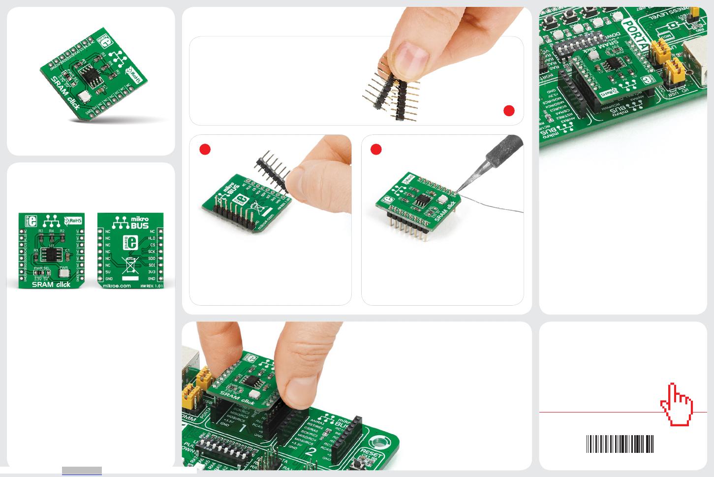
2. Soldering the headers
3. Plugging the board in
Once you have soldered the headers your
board is ready to be placed into the desired
mikroBUS™ socket. Make sure to align the cut
in the lower-right part of the board with the
markings on the silkscreen at the mikroBUS™
socket. If all the pins are aligned
correctly, push the board all the
way into the socket.
Turn the board upward again. Make sure
to align the headers so that they are
perpendicular to the board, then solder the
pins carefully.
Turn the board upside down so that
the bottom side is facing you upwards.
Place shorter pins of the header into the
appropriate soldering pads.
Before using your click board™, make sure
to solder 1x8 male headers to both left and
right side of the board. Two 1x8 male headers
are included with the board in the package.
4. Essential features
The 23LC1024 IC organizes the memory
in 8-bit instruction registers and 32-byte
pages. Three operating modes for reading
and writing data are available: byte, page, and
sequential (the last one allows read/write for
entire memory array). The clock rate for all
three modes is up to 20MHz. The HOLD pin,
when pulled low, suspends data transmission
mid-sequence (without causing the reset of
the entire sequence).
1
SRAM click lets you add 1 Mbit of additional
SRAM memory to your devices, via the
23LC1024 chip. The board communicates
with the target MCU through the mikroBUS™
SPI interface (MISO, MOSI, SCK, CS) with
additional HOLD functionality provided
through the default mikroBUS™ RST pin.
SRAM click is designed to use either a 3.3V
or 5V power supply.
SRAM click
1. Introduction
SRAM click manual
ver 1.01
0100000081969
Downloaded from Arrow.com.

