
To all our customers
Information regarding change of names mentioned
within this document, to Renesas Technology Corp.
On April 1
st
2003 the following semiconductor operations were transferred to
Renesas Technology Corporation: operations covering microcomputer, logic,
analog and discrete devices, and memory chips other than DRAMs (flash
memory, SRAMs etc.).
Accordingly, although Hitachi, Hitachi, Ltd., Hitachi Semiconductors, and other
Hitachi brand names are mentioned in the document, these names have all
been changed to Renesas Technology Corporation.
Except for our corporate trademark, logo and corporate statement, no
changes whatsoever have been made to the contents of the document, and
these changes do not constitute any alteration to the contents of the
document itself.
Thank you for your understanding.
Renesas Technology Home Page: www.renesas.com
Renesas Technology Corp.
April 1, 2003
Renesas Technology Corp.

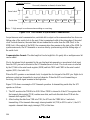
SuperH™ RISC Engine
SH7032 and SH7034
HD6417032, HD6477034,
HD6437034, HD6417034
HD6437034B, HD6417034B
Hardware Manual
ADE-602-062E
Rev. 6.0
9/18/02
Hitachi, Ltd.

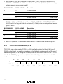
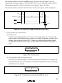
Cautions
1. Hitachi neither warrants nor grants licenses of any rights of Hitachi’s or any third party’s
patent, copyright, trademark, or other intellectual property rights for information contained in
this document. Hitachi bears no responsibility for problems that may arise with third party’s
rights, including intellectual property rights, in connection with use of the information
contained in this document.
2. Products and product specifications may be subject to change without notice. Confirm that you
have received the latest product standards or specifications before final design, purchase or
use.
3. Hitachi makes every attempt to ensure that its products are of high quality and reliability.
However, contact Hitachi’s sales office before using the product in an application that
demands especially high quality and reliability or where its failure or malfunction may directly
threaten human life or cause risk of bodily injury, such as aerospace, aeronautics, nuclear
power, combustion control, transportation, traffic, safety equipment or medical equipment for
life support.
4. Design your application so that the product is used within the ranges guaranteed by Hitachi
particularly for maximum rating, operating supply voltage range, heat radiation characteristics,
installation conditions and other characteristics. Hitachi bears no responsibility for failure or
damage when used beyond the guaranteed ranges. Even within the guaranteed ranges,
consider normally foreseeable failure rates or failure modes in semiconductor devices and
employ systemic measures such as fail-safes, so that the equipment incorporating Hitachi
product does not cause bodily injury, fire or other consequential damage due to operation of
the Hitachi product.
5. This product is not designed to be radiation resistant.
6. No one is permitted to reproduce or duplicate, in any form, the whole or part of this document
without written approval from Hitachi.
7. Contact Hitachi’s sales office for any questions regarding this document or Hitachi
semiconductor products.

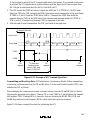
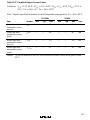
Preface
The SH7032 and SH7034 are microprocessors that integrate peripheral functions necessary for
system configuration with a 32-bit internal architecture SH1-DSP CPU as its core.
The SH7032 and SH7034's on-chip peripheral functions include an interrupt controller, timers,
serial communication interfaces, a user break controller (UBC), a bus state controller (BSC), a
direct memory access controller (DMAC), and I/O ports, making it ideal for use as a
microcomputer in electronic devices that require high speed together with low power
consumption.
Intended Readership: This manual is intended for users undertaking the design of an application
system using the SH7032 and SH7034. Readers using this manual require a
basic knowledge of electrical circuits, logic circuits, and microcomputers.
Purpose: The purpose of this manual is to give users an understanding of the hardware
functions and electrical characteristics of the SH7032 and SH7034. Details
of execution instructions can be found in the SH-1, SH-2, SH-DSP
Programming Manual, which should be read in conjunction with the present
manual.
Using this Manual:
• For an overall understanding of the SH7032 and SH7034's functions
Follow the Table of Contents. This manual is broadly divided into sections on the CPU, system
control functions, peripheral functions, and electrical characteristics.
• For a detailed understanding of CPU functions
Refer to the separate publication SH-1, SH-2, SH-DSP Programming Manual.
Note on bit notation: Bits are shown in high-to-low order from left to right.
Related Material: The latest information is available at our Web Site. Please make sure that you
have the most up-to-date information available.
http://www.hitachisemiconductor.com/

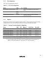
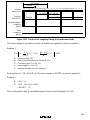
User's Manuals on the SH7032 and SH7034:
Manual Title ADE No.
SH7032 and SH7034 Hardware Manual This manual
SH-1, SH-2, SH-DSP Programming Manual ADE-602-085
Users manuals for development tools:
Manual Title ADE No.
C/C++ Complier, Assembler, Optimized Linkage Editor User's Manual ADE-702-304
Simulator Debugger Users Manual ADE-702-266
Hitachi Embedded Workshop Users Manual ADE-702-275
Application Note:
Manual Title ADE No.
C/C++ Complier ADE-502-046

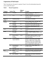
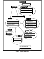
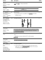
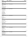
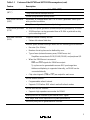
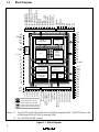
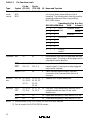
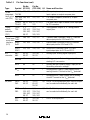
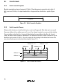
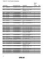
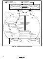
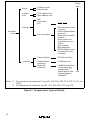
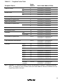
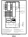
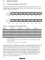
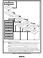
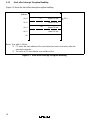
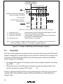
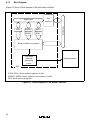
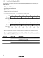
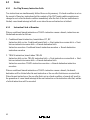
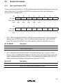
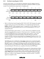
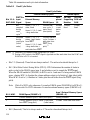
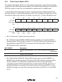
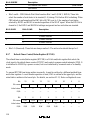
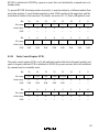
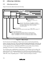
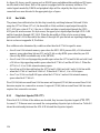
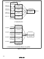
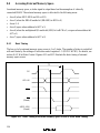
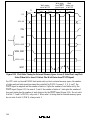
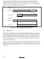
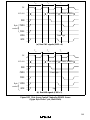
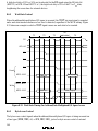
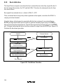
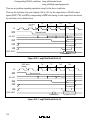
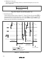
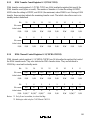
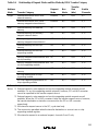
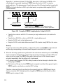
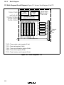
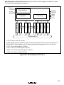
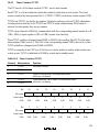
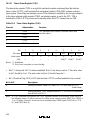
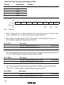
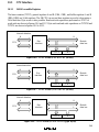
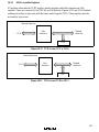
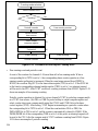
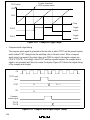
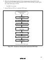
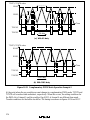
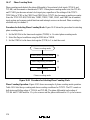
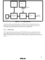
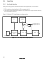
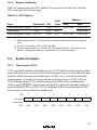
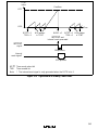
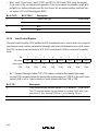
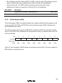
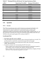
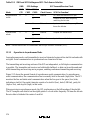
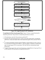
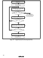
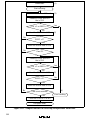
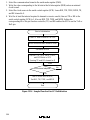
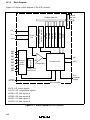
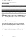
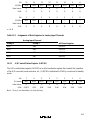
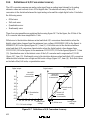
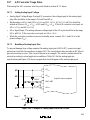
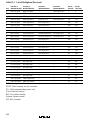
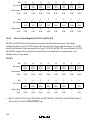
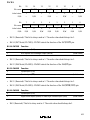
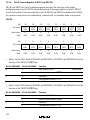
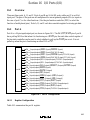
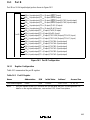
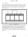
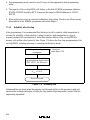
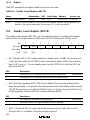
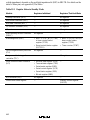
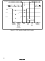
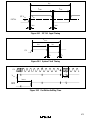
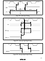
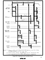
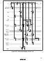
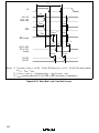
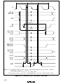
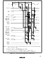
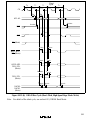
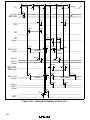
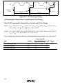
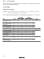
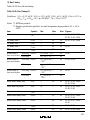
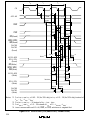
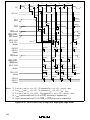
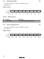
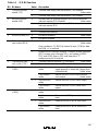
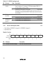
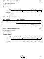
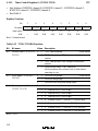
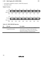
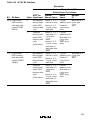
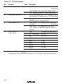
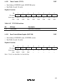
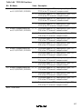
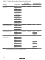
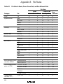
Organization of This Manual
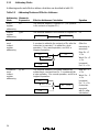
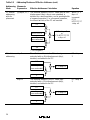
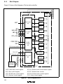
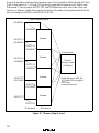
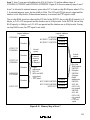
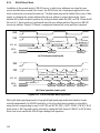
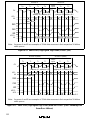
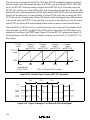
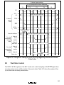
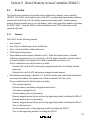
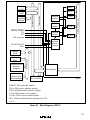
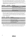
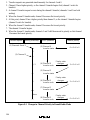
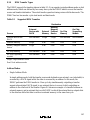
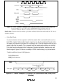
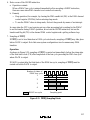
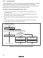
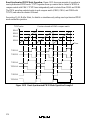
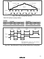
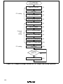
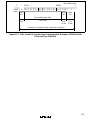
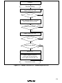
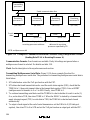
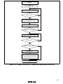
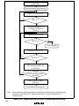
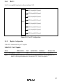
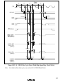
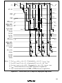
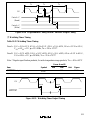
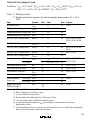
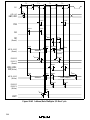
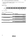
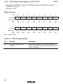
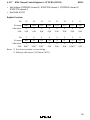
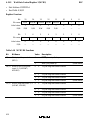
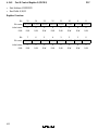
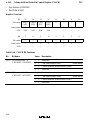
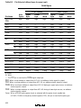
Table 1 describes how this manual is organized. Figure 1 shows the relationships between the
sections within this manual.
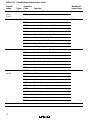
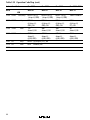
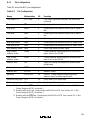
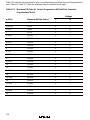
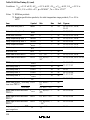
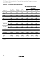
Table 1 Manual Organization
Category Section Title
Abbrevi-
ation Contents
Overview 1. Overview — Features, internal block diagram, pin
layout, pin functions
CPU 2. CPU CPU Register configuration, data structure.
instruction features, instruction types,
instruction lists
Operating
Modes
3. Operating Modes — MCU mode, PROM mode
Internal
Modules
4. Exception
Handling
— Resets, address errors, interrupts, trap
instructions, illegal instructions
5. Interrupt
Controller
INTC NMI interrupts, user break interrupts, IRQ
interrupts, on-chip module interrupts
6. User Break
Controller
UBC Break address and break bus cycle
selection
Clock 7. Clock Pulse
Generator
CPG Crystal pulse generator, duty correction
circuit
Buses 8. Bus State
Controller
BSC Division of memory space, DRAM
interface, refresh, wait state control, parity
control
9. Direct Memory
Access
Controller
DMAC Auto request, external request, on-chip
peripheral module request, cycle steal
mode, burst mode
Timers 10. 16-Bit Integrated
Timer Pulse Unit
ITU Waveform output mode, input capture
function, counter clear function, buffer
operation, PWM mode, complementary
PWM mode, reset synchronized mode,
synchronized operation, phase counting
mode, compare match output mode
11. Programmable
Timing Pattern
Controller
TPC Compare match output triggers, non-
overlap operation
12. Watchdog Timer WDT Watchdog timer mode, interval timer mode
Data
Processing
13. Serial
Communication
Interface
SCI Asynchronous mode, synchronous mode,
multiprocessor communication function
14. A/D Converter A/D Single mode, scan mode, activation by
external trigger

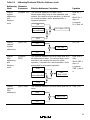
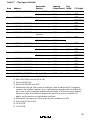
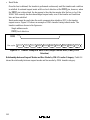
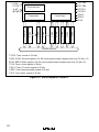
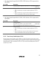
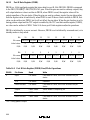
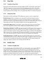
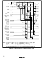
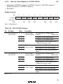
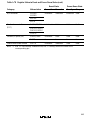
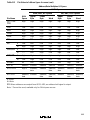
Table 1 Manual Organization (cont)
Category Section Title
Abbrevi-
ation Contents
Pins 15. Pin Function
Controller
PFC Pin function selection
16. Parallel I/O
Ports
I/O I/O ports
Memory 17. ROM ROM PROM mode, high-speed programming
system
18. RAM RAM On-chip RAM
Power-Down
State
19. Power-Down
State
— Sleep mode, standby mode
Electrical
Char act er i s t i c s
20. Electrical
Characteristics
— Absolute maximum ratings, AC
characteristics, DC characteristics,
operation timing

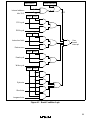
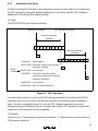
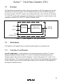
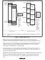
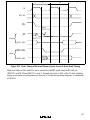
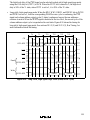
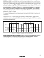
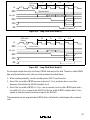
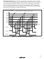
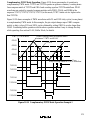
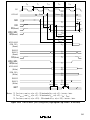
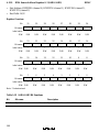
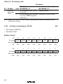
4. Exception handling
5. Interrupt controller (INTC)
6. User break controller (UBC)
On-chip modules
7. Clock pulse generator (CPG)
8. Bus state controller (BSC)
9. Direct memory access
controller (DMAC)
Buses
10. 16-bit integrated timer
pulse unit (ITU)
Timers
13. Serial communication
interface (SCI)
14. A/D converter
Data processing
15. Pin function
controller (PFC)
16. Parallel I/O ports
Pins
17. ROM
18. RAM
Memory
19. Power-down state
20. Electrical characteristics
1. Overview
2. CPU
3. Operating modes
11. Programmable timing
pattern controller (TPC)
12. Watchdog timer (WDT)
Figure 1 Manual Organization

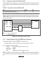
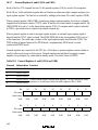
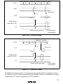
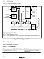
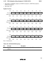
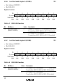
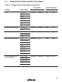
Addresses of On-Chip Peripheral Module Registers
The on-chip peripheral module registers are located in the on-chip peripheral module space (area
5: H'5000000–H'5FFFFFF), but since the actual register space is only 512 bytes, address bits
A23–A9 are ignored. 32k shadow areas in 512 byte units that contain exactly the same contents as
the actual registers are thus provided in the on-chip peripheral module space.
In this manual, register addresses are specified as though the on-chip peripheral module registers
were in the 512 bytes H'5FFFE00–H'5FFFFFF. Only the values of the A27–A24 and A8–A0 bits
are valid; the A23–A9 bits are ignored. When area H'5000000–H'50001FF is accessed, for
example, the result will be the same as when area H'5FFFE00–H'5FFFFFF is accessed. For more
details, see Section 8.3.5, Area Descriptions: Area 5.

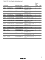
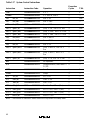
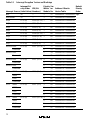
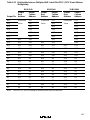
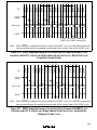
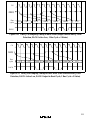
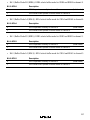
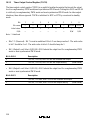
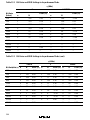
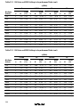
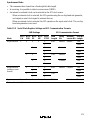
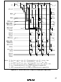
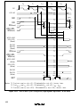
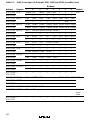
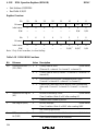
List of Items Revised or Added for This Version
Section Page Description Edition
1.1 SuperH
Microcomputer
Features
Table 1.2 Product
Lineup
6, 7 SH7034, SH7032: 2 to 16.6 MHz device deleted.
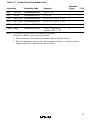
Product
Number
On-Chip
ROM
Operating
Voltage
Operating
Frequency
Temperature
Range Model
Marking
Model No.
*
2
Package
SH7032 ROMless 5.0 V 2 to 20 MHz -20 to +75°C HD6417032F20 HD6417032F20 112-pin plastic
-40 to +85°C HD6417032FI20 HD6417032FI20
QFP (FP-112)
3.3 V 2 to 12.5 MHz -20 to +75°C HD6417032VF12 HD6417032VF12
-40 to +85°C HD6417032VFI12 HD6417032VFI12
5.0 V 2 to 20 MHz -20 to +75°C HD6417032X20 HD6417032TE20 120-pin plastic
-40 to +85°C HD6417032XI20 HD6417032TEI20
TQFP (TFP-120)
3.3 V 2 to 12.5 MHz -20 to +75°C HD6417032VX12 HD6417032VTE12
-40 to +85°C HD6417032VXI12 HD6417032VTEI12
SH7034 PROM 5.0 V 2 to 20 MHz -20 to +75°C HD6477034F20 HD6477034F20 112-pin plastic
-40 to +85°C HD6477034FI20 HD6477034FI20
QFP (FP-112)
3.3 V 2 to12.5 MHz -20 to +75°C HD6 4 7 70 3 4 V F1 2 HD6 4 7 70 3 4 V F1 2
-40 to +85°C HD6 4 7 70 3 4 V FI 1 2 HD6 4 7 70 3 4 V FI 1 2
5.0 V 2 to 20 MHz -20 to +75°C HD6477034X20 HD6 4 7 70 3 4 TE 2 0 120-pin plastic
-40 to +85°C HD6477034XI20 HD6 4 7 70 3 4 TE I 2 0
TQFP (TFP-120)
3.3 V 2 to 12.5 MHz -20 to +75°C HD6 4 7 70 3 4 V X 1 2 HD6 4 7 70 3 4 V TE 1 2
-40 to +85°C HD6 4 7 70 3 4 V X I 1 2 HD6 4 7 70 3 4 V TE I 1 2
Mask 5.0 V 2 to 20 MHz -20 to +75°C HD6437034AF20 HD6437034AF20 112-pin plastic
ROM
-40 to +85°C HD6437034AFI20 HD6437034AFI20
QFP (FP-112)
3.3 V 2 to 12.5 MHz -20 to +75°C HD6437034AVF12 HD6437034AF12
-40 to +85°C HD6437034AVFI12 HD6437034AFI12
5.0 V 2 to 20 MHz -20 to +75°C HD6437034AX20 HD6437034ATE20 120-pin plastic
-40 to +85°C HD6437034AXI20 HD6437034ATEI20
TQFP (TFP-120)
3.3 V 2 to 12.5 MHz -20 to +75°C HD6437 0 3 4 A VX 1 2 HD6437034ATE12
-40 to +85°C HD6437034AVXI12 HD6437034ATEI12
ROMless 5.0 V 2 to 20 MHz -20 to +75°C HD6417034F20 HD6417034F20 112-pin plastic
-40 to +85°C HD6417034FI20 HD6417034FI20
QFP (FP-112)
3.3 V 2 to 12.5 MHz -20 to +75°C HD6417034VF12 HD6417034VF12
-40 to +85°C HD6417034VFI12 HD6417034VFI12
5.0 V 2 to 20 MHz -20 to +75°C HD6417034X20 HD6417034TE20 120-pin plastic
-40 to +85°C HD6417034XI20 HD6417034TEI20
TQFP (TFP-120)
3.3 V 2 to 12.5 MHz -20 to +75°C HD6417034VX12 HD6417034VTE12
-40 to +85°C HD6417034VXI12 HD6417034VTEI12
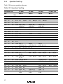
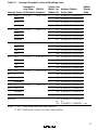
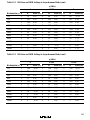
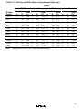
Product
Number
On-Chip
ROM
Operating
Voltage
Operating
Frequency
Temperature
Range Model
Marking
Model No.
*
2
Package
SH7034B
*
1
Mask 3.3 V 4 to 12.5 MHz -20 to +75°C HD6437034BVF12 6437034B(***)F 112-pin plastic
ROM
-40 to +85°C HD6437034BVFW12 6437034B(***)FW
QFP (FP-112)
-20 to +75°C HD6437034BVX12 6437034B(***)X 120-pin plastic
-40 to +85°C HD6437034BVXW12 6437034B(***)XW
TQFP (TFP-120)
ROMless 3.3 V 4 to 20 MHz -20 to +75°C HD6417034BVF20 HD6417034BVF20 112-pin plastic
-40 to +85°C HD6417034BVFW20 HD6417034BVFW20
QFP (FP-112)
-20 to +75°C HD6417034BVX20 6417034BVTE20 120-pin plastic
-40 to +85°C HD6417034BVXW20 6417034BVTEW20
TQFP (TFP-120)
Notes: *1 The electrical characteristics of the SH7034B mask ROM version and SH7034 PROM
version are different.
*2 For mask ROM versions, (***) is the ROM code.
6
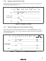
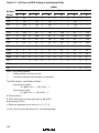
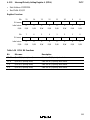
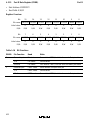
1.3.2 Pin Functions
Table 1.3 Pin
Functions
12 Note amended
*2 Can be used in the SH7034 PROM version.
6

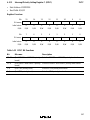
Section Page Description Edition
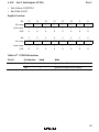
2.1.2 Control
Registers
Figure 2.2 Control
Registers
18 Description amended
Bits I3–I0: Interrupt mask bits.
6
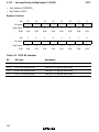
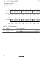
2.1.4 Initial Values
of Registers
Table 2.1 Initial
Values of Registers
19 Description amended
SR Bits I3–I0 are 1111(H'F), reserved bits are 0, and other
bits are undefined
6
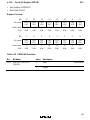
3.1 Types of
Operating Modes and
Their Selection
Table 3.1 Operating
Mode Selection
49 Note amended
*2 Only modes 0 and 1 are available in the SH7032 and SH7034
ROMless version.
6
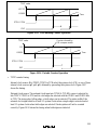
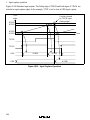
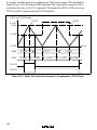
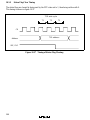
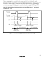
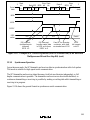
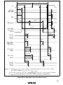
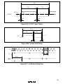
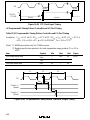
8.11.3 Maximum
Number of States
from BREQ Input to
Bus Release
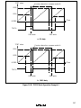
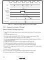
Figure 8.47 Bus
Release Procedure
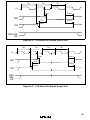
174 Description amended
t
BACD2
t
BRQS
t
BACD1
6
9.1.4 Register
Configuration
Table 9.2 DMAC
Registers
179 *4 added
*4 Only the values of bits A27–A24 and A8–A0 are valid; bits A23–A9
are ignored. For details on the register addresses, see section
8.3.5, Area Descriptions.
6
9.3.4 DMA Transfer
Types
200 Description amended
Line 3
⋅⋅⋅ destination or source must be the SCI or A/D converter
(table 9.4). ⋅⋅⋅
6
10.1.4 Register
Configuration
Table 10.3 Register
Configuration
230 *2 description amended
*2 Only 0 can be written to clear flags.
6
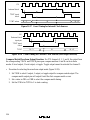
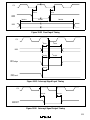
10.4.5 Reset-
Synchronized PWM
Mode
Procedure for
Selecting Reset-
Synchronized PWM
Mode (figure 10.31):
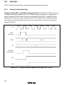
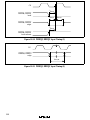
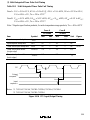
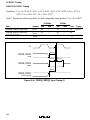
268 Description amended
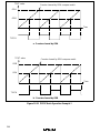
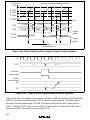
4. Set bits CMD1 and CMD0 in TFCR to select reset-synchronized
PWM mode. TIOCA3, TIOCB3, TIOCA4, TIOCB4, TOCXA4, and
TOCXB4 become PWM output pins.
6

Section Page Description Edition
10.4.6
Complementary
PWM Mode
Procedure for
Selecting
Complementary
PWM Mode (Figure
10.33):
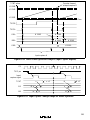
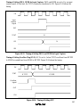
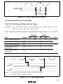
271 Description amended
3. Set bits CMD1 and CMD0 in TMDB to select complementary PWM
mode. TIOCA3, TIOCB3, TIOCA4, TIOCB4, TOCXA4, and
TOCXB4 become PWM pins.
6
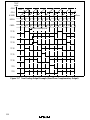
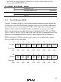
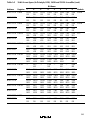
10.6.15 ITU
Operating Modes
Table 10.18 ITU
Operating Modes
(Channel 0)
301 Table amended
Register Setting
TSNC TMDR TFCR TOCR TIOR0 TCR0
Operating
Mode Sync MDF FDIR PWM
Comp
PWM
Reset
Sync
PWM Buffer
Output
Level
Select IOA IOB
Clear
Select
Clock
Select
Synch-
ronized
preset
SYNC0
= 1
——√ ——— — √√ √√
PWM √ — — PWM0
= 1
——— — — √ * √√
Output
compare A
function
√ — — PWM0
= 0
— — — — IOA2 = 0,
others:
don’t care
√√√
6
Table 10.19 ITU
Operating Modes
(Channel 1)
302 Table amended
Register Setting
TSNC TMDR TFCR TOCR TIOR1 TCR1
Operating
Mode Sync MDF FDIR PWM
Comp
PWM
Reset
Sync
PWM Buffer
Output
Level
Select IOA IOB
Clear
Select
Clock
Select
Synch-
ronized
preset
SYNC1
= 1
——√ ——— — √√ √√
PWM √ — — PWM1
= 1
——— — — √
*
√√
Output
compare A
function
√ — — PWM1
= 0
— — — — IOA2 = 0,
others:
don’t care
√√√
6
Table 10.20 ITU
Operating Modes
(Channel 2)
303 Table amended
Register Setting
TSNC TMDR TFCR TOCR TIOR2 TCR2
Operating
Mode Sync MDF FDIR PWM
Comp
PWM
Reset
Sync
PWM Buffer
Output
Level
Select IOA IOB
Clear
Select
Clock
Select
Synch-
ronized
preset
SYNC2
= 1
——√ ——— — √√ √√
PWM √ — — PWM2
= 1
——— — — √
*
√√
Output
compare A
function
√ — — PWM2
= 0
— — — — IOA2 = 0,
others:
don’t care
√√√
6
12.1.4 Register
Configuration
Table 12.2 WDT
Registers
337 *4 added
Initial
Address
*
4
Name Abbreviation R/W Value Write
*
1
Read
*
2
Timer control/status register TCSR R/(W)
*
3
H'18 H'5FFFFB8 H'5FFFFB8
Timer counter TCNT R/W H'00 H'5FFFFB9
Reset control/status register RSTCSR R/(W)
*
3
H'1F H'5FFFFBA H'5FFFFBB
Notes: *1 Write by word transfer. A byte or longword write cannot be used.
*2 Read by byte transfer. The correct value cannot be obtained by a word or longword
read.
*3 Only 0 can be written in bit 7, to clear the flag.
*4 Only the values of bits A27–A24 and A8–A0 are valid; bits A23–A9 are ignored. For
details on the register addresses, see section 8.3.5, Area Descriptions
6

Section Page Description Edition
12.2.2 Timer
Control/Status
Register (TCSR)
338 Note added
Note: * Only 0 can be written, to clear the flag.
6
13.2.6 Serial Control
Register
359 Initial value added
Internal clock, SCK pin used for input pin (input signal
is ignored) or output pin (output level is undefined)
*
2
(Initial value)
Internal clock, SCK pin used for serial clock output
*
2
(Initial value)
6
13.2.8 Bit Rate
Register (BRR)
Table 13.3 Bit Rates
and BRR Settings in
Asynchronous Mode
367 Note added
Note: Settings with an error of 1% or less are recommended.
6
Table 13.4 Bit
Rates and BRR
Settings in
Synchronous Mode
368 Note deleted 6
15.2 Register
Configuration
Table 15.2 Pin
Function Controller
Registers
427 Note added
Name Abbreviation R/W Initial Value Address* Access Size
Port A I/O register PAIOR R/W H'0000 H'5FFFFC4 8, 16, 32
Port A control register 1 PACR1 R/W H'3302 H'5FFFFC8 8, 16, 32
Port A control register 2 PACR2 R/W H'FF95 H'5FFFFCA 8, 16, 32
Port B I/O register PBIOR R/W H'0000 H'5FFFFC6 8, 16, 32
Port B control register 1 PBCR1 R/W H'0000 H'5FFFFCC 8, 16, 32
Port B control register 2 PBCR2 R/W H'0000 H'5FFFFCE 8, 16, 32
Column address strobe
pin control register
CASCR R/W H'5FFF H'5FFFFEE 8, 16, 32
Note: * Only the values of bits A27–A24 and A8–A0 are valid; bits A23–A9 are ignored. For
details on the register addresses, see section 8.3.5, Area Descriptions.
6
16.2.1 Register
Configuration
Table 16.1 Port A
Register
442 Note added
Name Abbreviation R/W Initial Value Address* Access Size
Port A data register PADR R/W H'0000 H'5FFFFC0 8, 16, 32
Note: * Only the values of bits A27–A24 and A8–A0 are valid; bits A23–A9 are ignored. For
details on the register addresses, see section 8.3.5, Area Descriptions.
6
16.3.1 Register
Configuration
Table 16.3 Port B
Register
443 Note added
Name Abbreviation R/W Initial Value Address* Access Size
Port B data register PBDR R/W H'0000 H'5FFFFC2 8, 16, 32
Note: * Only the values of bits A27–A24 and A8–A0 are valid; bits A23–A9 are ignored. For
details on the register addresses, see section 8.3.5, Area Descriptions.
6
16.4.1 Register
Configuration
Table 16.5 Port C
Register
445 Note added
Name Abbreviation R/W Initial Value Address* Access Size
—
Note: * Only the values of bits A27–A24 and A8–A0 are valid; bits A23–A9 are ignored. For
details on the register addresses, see section 8.3.5, Area Descriptions.
Port C data register PCDR R/W H'5FFFFD0 8, 16, 32
6

Section Page Description Edition
19.1.2 Register
Table 19.2 Standby
Control Register
(SBYCR)
460 Note added
Name Abbreviation R/W Initial Value Address* Access size
Standby control register SBYCR R/W H'1F H'5FFFFBC 8, 16, 32
Note: * Only the values of bits A27–A24 and A8–A0 are valid; bits A23–A9 are ignored. For
details on the register addresses, see section 8.3.5, Area Descriptions.
6
20.1.2 DC
Characteristics
Table 20.2 DC
Characteristics
467 16.6 MHz deleted 6
Table 20. 2 DC
Characteristics
Table of 16.6 MHz deleted 6
Table 20.3
Permitted Output
Current Values
471 16.6 MHz deleted 6
20.1.3 AC
Characteristics
(1) Clock Timing
Table 20.4 Clock
Timing
472 16.6 MHz deleted 6
(2) Control Signal
Timing
Table 20.5 Control
Signal Timing
474 16.6 MHz deleted 6
(3) Bus Timing
Table 20.6 Bus
Timing (1)
478,
479
Description amended
Read data access time 1
*
6
t
ACC1
t
cyc
– 30
*
4
— ns 20.8, 20.11, 20.12
Read data access time 2
*
6
t
ACC2
t
cyc
× (n+2) –
30
*
3
— ns 20.9, 20.10,
20.13–20.15
Read data access time from
CAS 2
*
6
t
CAC2
t
cyc
× (n+1) –
25
*
3
—ns
Read data access time from
RAS 1
*
6
t
RAC1
t
cyc
× 1.5 – 20 — ns 20.11, 20.12
Read data access time from
RAS 2
*
6
t
RAC2
t
cyc
× (n+2.5)
– 20
*
3
—ns
20.13–20.15
20.13–20.15
Data setup time for CAS t
DS
0
*
5
— ns 20.11, 20.13
CAS setup time for RAS t
CSR
10 — ns 20.16–20.18
Row address hold time t
RAH
10 — ns 20.11, 20.13
6
Table 20.7 Bus
Timing (2)
Table deleted
6
Table 20.7 Bus
Timing (2)
494 Description amended
Read data access time 1
*
4
t
ACC1
t
cyc
– 44 — ns 20.21, 20.24, 20.25
Read data access time 2
*
4
t
ACC2
t
cyc
× (n+2) – 44
*
2
— ns 20.22, 20.23,
20.26–20.28
6

Section Page Description Edition
(4) DMAC Timing
Table 20.8 DMAC
Timing
507 16.6 MHz deleted 6
(5) 16-bit Integrated
Timer Pulse Unit
Timing
Table 20.9 16-bit
Integrated Timer
Pulse Unit Timing
509 16.6 MHz deleted 6
(6) Programmable
Timing Pattern
Controller and I/O
Port Timing
Table 20.10
Programmable
Timing Pattern
Controller and I/O
Port Timing
510 16.6 MHz deleted 6
(7) Watchdog Timer
Timing
Table 20.11
Watchdog Timer
Timing
511 16.6 MHz deleted
6
(8) Serial
Communication
Interface Timing
Table 20.12 Serial
Communication
Interface Timing
512 16.6 MHz deleted
6
(9) A/D Converter
Timing
Table 20.13 A/D
Converter Timing
513 16.6 MHz deleted
6
20.1.4 A/D
Converter
Characteristics
Table 20.14 A/D
Converter
Characteristics
516 16.6 MHz deleted
6
20.2 SH7034B 3.3 V
12.5 MHz Version
and 20 MHz
Version
*
1
Electrical
Characteristics
517 12.5 MHz added 6

Section Page Description Edition
20.2.1 Absolute
Maximum Ratings
Table 20.15
Absolute Maximum
Ratings
517 Notes amended
Item Symbol Rating Unit
Power supply voltage V
CC
–0.3 to +4.6 V
Input voltage (except port C) V
in
–0.3 to V
CC
+ 0.3 V
Input voltage (port C) V
in
–0.3 to AV
CC
+ 0.3 V
Analog power supply voltage AV
CC
–0.3 to +4.6 V
Analog reference voltage AV
ref
–0.3 to AV
CC
+ 0.3 V
Analog input voltage V
AN
–0.3 to AV
CC
+ 0.3 V
Operating temperature T
opr
–20 to +75
*
2
˚C
Storage temperature T
stg
–55 to +125 ˚C
Caution: Operating the chip in excess of the absolute maximum rating may result in permanent
damage.
Notes: *1 ROMless products only for 20 MHz version
*2 Regular-specification products; for wide-temperature-range products, Topr = –40 to
+85°C
6
Table 20.16 DC
Characteristics
518,
519
12.5 MHz added
Conditions: V
CC
= 3.3 V ±0.3V, AV
CC
= 3.3 V ±0.3V, AV
CC
= V
CC
±0.3V, AV
ref
= 3.0 V to
AV
CC
, V
SS
= AV
SS
= 0 V, φ = 12.5 to 20 MHz
*
1
, Ta = –20 to +75°C
*
2
Notes: *1 ROMless products only for 20 MHz version
*2 Regular-specification products; for wide-temperature-range products, Ta = –40 to
+85°C
Current Ordinary I
CC
— 25 — mA f = 12.5 MHz
consumption operation
— 35 60 mA f = 20 MHz
Sleep — 20 — mA f = 12.5 MHz
— 30 40 mA f = 20 MHz
Standby — 0.1 5 µA Ta ≤ 50°C
——10 µA50°C < Ta
6
Table 20.17
Permitted Output
Current Values
521 12.5 MHz added
12.5 MHz 20 MHz
Item Symbol Min Typ Max Min Typ Max Unit
Output low-level
permissible current
(per pin)
I
OL
——10 ——10mA
Output low-level
permissible current
(total)
∑ I
OL
——80 ——80mA
Output high-level
permissible current
(per pin)
–I
OH
——2.0 ——2.0mA
Output high-level
permissible current
(total)
–∑ I
OH
——25 ——25mA
Caution: To ensure reliability of the chip, do not exceed the output current values given in table
20.18.
6

Section Page Description Edition
20.2.3 AC
Characteristics
(1) Clock Timing
Table 20.18 Clock
Timing
522 12.5 MHz added and description amended
12.5 MHz 20 MHz
Item Symbol Min Max Min Max Unit Figures
EXTAL input high level
pulse width
t
EXH
22 — 15 — ns 20.45
EXTAL input low level
pulse width
t
EXL
22 — 15 — ns
EXTAL input rise time t
EXr
—10 —5 ns
EXTAL input fall time t
EXf
—10 —5 ns
Clock cycle time t
cyc
80 500 50 250 ns 20.45, 20.46
Clock high pulse width t
CH
30 — 20 — ns 20.46
Clock low pulse width t
CL
30 — 20 — ns
Clock rise time t
Cr
—10 —5 ns
Clock fall time t
Cf
—10 —5 ns
Reset oscillation settling
time
t
OSC1
10 — 10 — ms 20.47
Software standby
oscillation settling time
t
OSC2
10 — 10 — ms
6
(2) Control Signal
Timing
Table 20.19 Control
Signal Timing
524 12.5 MHz added and description amended
12.5 MHz 20 MHz
Item Symbol Min Max Min Max Unit Figure
RES setup time t
RESS
320 — 200 — ns 20.48
RES pulse width t
RESW
20 — 20 — t
cyc
NMI reset setup time t
NMIRS
320 — 200 — ns
NMI reset hold time t
NMIRH
320 — 200 — ns
NMI setup time t
NMIS
160 — 100 — ns 20.49
NMI hold time t
NMIH
80 — 50 — ns
IRQ0–IRQ7 setup time
(edge detection)
t
IRQES
160 — 100 — ns
IRQ0–IRQ7 setup time
(level detection)
t
IRQLS
160 — 100 — ns
IRQ0–IRQ7 hold time t
IRQEH
80 — 50 — ns
IRQOUT output delay
time
t
IRQOD
— 80 — 50 ns 20.50
Bus request setup time t
BRQS
80 — 50 — ns 20.51
Bus acknowledge delay
time 1
t
BACD1
— 80 — 50 ns
Bus acknowledge delay
time 2
t
BACD2
— 80 — 50 ns
Bus 3-state delay time t
BZD
— 80 — 50 ns
6
(3) Bus Timing
Table 20.20 Bus
Timing (1)
528 Description amended
Read data access time 2
*
6
t
ACC2
t
cyc
× (n+2) –
30
*
3
— ns 20.53, 20.54, 20.57–20.59
6
(3) Bus Timing
Table 20.20 Bus
Timing (2)
530 to
532
Newly added 6

Section Page Description Edition
(4) DMAC Timing
Table 20.21 DMAC
Timing
546 12.5 MHz added
12.5 MHz 20 MHz
Item Symbol Min Max Min Max Unit Figure
DREQ0, DREQ1 setup time t
DRQS
80 — 27 — ns 20.65
DREQ0, DREQ1 hold time t
DRQH
30 — 30 — ns
DREQ0, DREQ1 Pulse width t
DRQW
1.5 — 1.5 — t
cyc
20.66
6
(5) 16-bit Integrated
Timer Pulse Unit
Timing
Table 20.22 16-bit
Integrated Timer
Pulse Unit Timing
547 12.5 MHz added
12.5 MHz 20 MHz
Item Symbol Min Max Min Max Unit Figure
Output compare delay time t
TOCD
— 100 — 100 ns 20.67
Input capture setup time t
TICS
50 — 35 — ns
Timer clock input setup time t
TCKS
50 — 50 — ns 20.68
Timer clock pulse width
(single edge)
t
TCKWH/L
1.5 — 1.5 — t
cyc
Timer clock pulse width
(both edges)
t
TCKWL/L
2.5 — 2.5 — t
cyc
6
(6) Programmable
Timing Pattern
Controller and I/O
Port Timing
Table 20.23
Programmable
Timing Pattern
Controller and I/O
Port Timing
548 Description amended
Conditions: V
CC
= 3.3 V ±0.3V, AV
CC
= 3.3 V ±0.3V, AV
CC
= V
CC
±0.3V, AV
ref
= 3.0 V to
AV
CC
, V
SS
= AV
SS
= 0 V, φ = 12.5 to 20 MHz
*
1
, Ta = –20 to +75°C
*
2
Notes: *1 ROMless products only for 20 MHz version
*2 Regular-specification products; for wide-temperature-range products, Ta = –40 to
+85°C
6
(7) Watchdog Timer
Timing
Table 20.24
Watchdog Timer
Timing
549 Description amended
Conditions: V
CC
= 3.3 V ±0.3V, AV
CC
= 3.3 V ±0.3V, AV
CC
= V
CC
±0.3V, AV
ref
= 3.0 V to
AV
CC
, V
SS
= AV
SS
= 0 V, φ = 12.5 to 20 MHz
*
1
, Ta = –20 to +75°C
*
2
Notes: *1 ROMless products only for 20 MHz version
*2 Regular-specification products; for wide-temperature-range products, Ta = –40 to
+85°C
6
(8) Serial
Communication
Interface Timing
Table 20.25 Serial
Communication
Interface Timing
550 Description amended
Conditions: V
CC
= 3.3 V ±0.3V, AV
CC
= 3.3 V ±0.3V, AV
CC
= V
CC
±0.3V, AV
ref
= 3.0 V to
AV
CC
, V
SS
= AV
SS
= 0 V, φ = 12.5 to 20 MHz
*
1
, Ta = –20 to +75°C
*
2
Notes: *1 ROMless products only for 20 MHz version
*2 Regular-specification products; for wide-temperature-range products, Ta = –40 to
+85°C
6
(9) A/D Converter
Timing
Table 20.26 A/D
Converter Timing
551 Description amended
Conditions: V
CC
= 3.3 V ±0.3V, AV
CC
= 3.3 V ±0.3V, AV
CC
= V
CC
±0.3V, AV
ref
= 3.0 V to
AV
CC
, V
SS
= AV
SS
= 0 V, φ = 12.5 to 20 MHz
*
1
, Ta = –20 to +75°C
*
2
Notes: *1 ROMless products only for 20 MHz version
*2 Regular-specification products; for wide-temperature-range products, Ta = –40 to
+85°C
6

Section Page Description Edition
20.2.4 A/D
Converter
Characteristics
Table 20.27 A/D
Converter
Characteristics
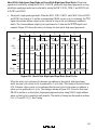
554 12.5 MHz added
12.5 MHz 20 MHz
Item Min Typ Max Min Typ Max Unit
Resolution 101010 101010bit
Conversion time — — 11.2 — — 6.7 µS
Analog input capacitance — — 20 — — 20 pF
Permissible signal-source impedance — — 1 — — 1 kΩ
Nonlinearity error* ——±4.0 — — ±4.0 LSB
Offset error* ——±4.0 — — ±4.0 LSB
Full-scale error* ——±4.0 — — ±4.0 LSB
Quantization error* ——±0.5 — — ±0.5 LSB
Absolute accuracy — — ±6.0 — — ±6.0 LSB
Note: *Reference value
6
A.2.17 Timer Status
Registers 0–4
(TSR0–TSR4)
Table A.18 TSR0–
TSR4 Bit Functions
581 Bit amended
Bit Bit name Value Description
2 Overflow flag (OVF) 0 Clear conditions: 0 is written in OVF after
reading OVF = 1 (Initial value)
1 Set conditions: TCNT value overflows (H'FFFF
? H'0000) or underflows (H'FFFF ? H'0000)
1 Input capture/compare match
flag B (IMFB)
0 Clear conditions: 0 is written in IMFB after
reading IMFB = 1 (Initial value)
1 Set conditions: (1) When GRB is functioning as
the output compare register, and TCNT = GRB;
(2) When GRB is functioning as the input
capture register, and the TCNT value is
transferred to GRB by the input capture signal
0 Input capture/compare match
flag A (IMFA)
0 Clear conditions: 0 is written in IMFA after
reading IMFA = 1 (Initial value)
1 Set conditions: (1) When GRA is functioning as
the output compare register, and TCNT = GRA;
(2) When GRA is functioning as the input
capture register, and the TCNT value is
transferred to GRA by the input capture signal
6
A.2.23 Timer Output
Control Register
(TOCR)
Table A.24 TOCR
Bit Functions
587 Table amended
Bit Bit name Value Description
1 Output level select 4 (OLS4) 0 Reverse output of TIOCA3, TIOCA4, TIOCB4
1 Direct output of TIOCA3, TIOCA4, TIOCB4
(Initial value)
0 Output level select 3 (OLS3) 0 Reverse output of TIOCB3, TOCXA4, TOCXB4
1 Direct output of TIOCB3, TOCXA4, TOCXB4
(Initial value)
6

Section Page Description Edition
A.3 Register Status
in Reset and Power-
Down States
Table A.77 Register
Status in Reset and
Power-Down States
644 *2 added
Watchdog timer (WDT) TCNT Initialized Initialized Held Held
TCSR
*
1
RSTCR
*
2
Initialized
Serial communication SMR Initialized Initialized Initialized Held
interface (SCI)
BRR
SCR
TDR
TSR Held
SSR Initialized
RDR
RSR Held
Notes: *1 Bits 7–5 (OVF, WT/IT, TME) are initialized, bits 2–0 (CKS2–CKS0) are held.
*2 Not initialized in the case of a reset by the WDT.
6
Page is loading ...
Page is loading ...
Page is loading ...
Page is loading ...
Page is loading ...
Page is loading ...
Page is loading ...
Page is loading ...
Page is loading ...
Page is loading ...
Page is loading ...
Page is loading ...
Page is loading ...
Page is loading ...
Page is loading ...
Page is loading ...
Page is loading ...
Page is loading ...
Page is loading ...
Page is loading ...
Page is loading ...
Page is loading ...
Page is loading ...
Page is loading ...
Page is loading ...
Page is loading ...
Page is loading ...
Page is loading ...
Page is loading ...
Page is loading ...
Page is loading ...
Page is loading ...
Page is loading ...
Page is loading ...
Page is loading ...
Page is loading ...
Page is loading ...
Page is loading ...
Page is loading ...
Page is loading ...
Page is loading ...
Page is loading ...
Page is loading ...
Page is loading ...
Page is loading ...
Page is loading ...
Page is loading ...
Page is loading ...
Page is loading ...
Page is loading ...
Page is loading ...
Page is loading ...
Page is loading ...
Page is loading ...
Page is loading ...
Page is loading ...
Page is loading ...
Page is loading ...
Page is loading ...
Page is loading ...
Page is loading ...
Page is loading ...
Page is loading ...
Page is loading ...
Page is loading ...
Page is loading ...
Page is loading ...
Page is loading ...
Page is loading ...
Page is loading ...
Page is loading ...
Page is loading ...
Page is loading ...
Page is loading ...
Page is loading ...
Page is loading ...
Page is loading ...
Page is loading ...
Page is loading ...
Page is loading ...
Page is loading ...
Page is loading ...
Page is loading ...
Page is loading ...
Page is loading ...
Page is loading ...
Page is loading ...
Page is loading ...
Page is loading ...
Page is loading ...
Page is loading ...
Page is loading ...
Page is loading ...
Page is loading ...
Page is loading ...
Page is loading ...
Page is loading ...
Page is loading ...
Page is loading ...
Page is loading ...
Page is loading ...
Page is loading ...
Page is loading ...
Page is loading ...
Page is loading ...
Page is loading ...
Page is loading ...
Page is loading ...
Page is loading ...
Page is loading ...
Page is loading ...
Page is loading ...
Page is loading ...
Page is loading ...
Page is loading ...
Page is loading ...
Page is loading ...
Page is loading ...
Page is loading ...
Page is loading ...
Page is loading ...
Page is loading ...
Page is loading ...
Page is loading ...
Page is loading ...
Page is loading ...
Page is loading ...
Page is loading ...
Page is loading ...
Page is loading ...
Page is loading ...
Page is loading ...
Page is loading ...
Page is loading ...
Page is loading ...
Page is loading ...
Page is loading ...
Page is loading ...
Page is loading ...
Page is loading ...
Page is loading ...
Page is loading ...
Page is loading ...
Page is loading ...
Page is loading ...
Page is loading ...
Page is loading ...
Page is loading ...
Page is loading ...
Page is loading ...
Page is loading ...
Page is loading ...
Page is loading ...
Page is loading ...
Page is loading ...
Page is loading ...
Page is loading ...
Page is loading ...
Page is loading ...
Page is loading ...
Page is loading ...
Page is loading ...
Page is loading ...
Page is loading ...
Page is loading ...
Page is loading ...
Page is loading ...
Page is loading ...
Page is loading ...
Page is loading ...
Page is loading ...
Page is loading ...
Page is loading ...
Page is loading ...
Page is loading ...
Page is loading ...
Page is loading ...
Page is loading ...
Page is loading ...
Page is loading ...
Page is loading ...
Page is loading ...
Page is loading ...
Page is loading ...
Page is loading ...
Page is loading ...
Page is loading ...
Page is loading ...
Page is loading ...
Page is loading ...
Page is loading ...
Page is loading ...
Page is loading ...
Page is loading ...
Page is loading ...
Page is loading ...
Page is loading ...
Page is loading ...
Page is loading ...
Page is loading ...
Page is loading ...
Page is loading ...
Page is loading ...
Page is loading ...
Page is loading ...
Page is loading ...
Page is loading ...
Page is loading ...
Page is loading ...
Page is loading ...
Page is loading ...
Page is loading ...
Page is loading ...
Page is loading ...
Page is loading ...
Page is loading ...
Page is loading ...
Page is loading ...
Page is loading ...
Page is loading ...
Page is loading ...
Page is loading ...
Page is loading ...
Page is loading ...
Page is loading ...
Page is loading ...
Page is loading ...
Page is loading ...
Page is loading ...
Page is loading ...
Page is loading ...
Page is loading ...
Page is loading ...
Page is loading ...
Page is loading ...
Page is loading ...
Page is loading ...
Page is loading ...
Page is loading ...
Page is loading ...
Page is loading ...
Page is loading ...
Page is loading ...
Page is loading ...
Page is loading ...
Page is loading ...
Page is loading ...
Page is loading ...
Page is loading ...
Page is loading ...
Page is loading ...
Page is loading ...
Page is loading ...
Page is loading ...
Page is loading ...
Page is loading ...
Page is loading ...
Page is loading ...
Page is loading ...
Page is loading ...
Page is loading ...
Page is loading ...
Page is loading ...
Page is loading ...
Page is loading ...
Page is loading ...
Page is loading ...
Page is loading ...
Page is loading ...
Page is loading ...
Page is loading ...
Page is loading ...
Page is loading ...
Page is loading ...
Page is loading ...
Page is loading ...
Page is loading ...
Page is loading ...
Page is loading ...
Page is loading ...
Page is loading ...
Page is loading ...
Page is loading ...
Page is loading ...
Page is loading ...
Page is loading ...
Page is loading ...
Page is loading ...
Page is loading ...
Page is loading ...
Page is loading ...
Page is loading ...
Page is loading ...
Page is loading ...
Page is loading ...
Page is loading ...
Page is loading ...
Page is loading ...
Page is loading ...
Page is loading ...
Page is loading ...
Page is loading ...
Page is loading ...
Page is loading ...
Page is loading ...
Page is loading ...
Page is loading ...
Page is loading ...
Page is loading ...
Page is loading ...
Page is loading ...
Page is loading ...
Page is loading ...
Page is loading ...
Page is loading ...
Page is loading ...
Page is loading ...
Page is loading ...
Page is loading ...
Page is loading ...
Page is loading ...
Page is loading ...
Page is loading ...
Page is loading ...
Page is loading ...
Page is loading ...
Page is loading ...
Page is loading ...
Page is loading ...
Page is loading ...
Page is loading ...
Page is loading ...
Page is loading ...
Page is loading ...
Page is loading ...
Page is loading ...
Page is loading ...
Page is loading ...
Page is loading ...
Page is loading ...
Page is loading ...
Page is loading ...
Page is loading ...
Page is loading ...
Page is loading ...
Page is loading ...
Page is loading ...
Page is loading ...
Page is loading ...
Page is loading ...
Page is loading ...
Page is loading ...
Page is loading ...
Page is loading ...
Page is loading ...
Page is loading ...
Page is loading ...
Page is loading ...
Page is loading ...
Page is loading ...
Page is loading ...
Page is loading ...
Page is loading ...
Page is loading ...
Page is loading ...
Page is loading ...
Page is loading ...
Page is loading ...
Page is loading ...
Page is loading ...
Page is loading ...
Page is loading ...
Page is loading ...
Page is loading ...
Page is loading ...
Page is loading ...
Page is loading ...
Page is loading ...
Page is loading ...
Page is loading ...
Page is loading ...
Page is loading ...
Page is loading ...
Page is loading ...
Page is loading ...
Page is loading ...
Page is loading ...
Page is loading ...
Page is loading ...
Page is loading ...
Page is loading ...
Page is loading ...
Page is loading ...
Page is loading ...
Page is loading ...
Page is loading ...
Page is loading ...
Page is loading ...
Page is loading ...
Page is loading ...
Page is loading ...
Page is loading ...
Page is loading ...
Page is loading ...
Page is loading ...
Page is loading ...
Page is loading ...
Page is loading ...
Page is loading ...
Page is loading ...
Page is loading ...
Page is loading ...
Page is loading ...
Page is loading ...
Page is loading ...
Page is loading ...
Page is loading ...
Page is loading ...
Page is loading ...
Page is loading ...
Page is loading ...
Page is loading ...
Page is loading ...
Page is loading ...
Page is loading ...
Page is loading ...
Page is loading ...
Page is loading ...
Page is loading ...
Page is loading ...
Page is loading ...
Page is loading ...
Page is loading ...
Page is loading ...
Page is loading ...
Page is loading ...
Page is loading ...
Page is loading ...
Page is loading ...
Page is loading ...
Page is loading ...
Page is loading ...
Page is loading ...
Page is loading ...
Page is loading ...
Page is loading ...
Page is loading ...
Page is loading ...
Page is loading ...
Page is loading ...
Page is loading ...
Page is loading ...
Page is loading ...
Page is loading ...
Page is loading ...
Page is loading ...
Page is loading ...
Page is loading ...
Page is loading ...
Page is loading ...
Page is loading ...
Page is loading ...
Page is loading ...
Page is loading ...
Page is loading ...
Page is loading ...
Page is loading ...
Page is loading ...
Page is loading ...
Page is loading ...
Page is loading ...
Page is loading ...
Page is loading ...
Page is loading ...
Page is loading ...
Page is loading ...
Page is loading ...
Page is loading ...
Page is loading ...
Page is loading ...
Page is loading ...
Page is loading ...
Page is loading ...
Page is loading ...
Page is loading ...
Page is loading ...
Page is loading ...
Page is loading ...
Page is loading ...
Page is loading ...
Page is loading ...
Page is loading ...
Page is loading ...
Page is loading ...
Page is loading ...
Page is loading ...
Page is loading ...
Page is loading ...
Page is loading ...
Page is loading ...
Page is loading ...
Page is loading ...
Page is loading ...
Page is loading ...
Page is loading ...
Page is loading ...
Page is loading ...
Page is loading ...
Page is loading ...
Page is loading ...
Page is loading ...
Page is loading ...
Page is loading ...
Page is loading ...
Page is loading ...
Page is loading ...
Page is loading ...
Page is loading ...
Page is loading ...
Page is loading ...
Page is loading ...
Page is loading ...
Page is loading ...
Page is loading ...
Page is loading ...
Page is loading ...
Page is loading ...
Page is loading ...
Page is loading ...
Page is loading ...
Page is loading ...
Page is loading ...
Page is loading ...
Page is loading ...
Page is loading ...
Page is loading ...
Page is loading ...
Page is loading ...
Page is loading ...
Page is loading ...
Page is loading ...
Page is loading ...
Page is loading ...
Page is loading ...
Page is loading ...
Page is loading ...
Page is loading ...
Page is loading ...
Page is loading ...
Page is loading ...
Page is loading ...
Page is loading ...
Page is loading ...
Page is loading ...
Page is loading ...
Page is loading ...
Page is loading ...
Page is loading ...
Page is loading ...
Page is loading ...
Page is loading ...
Page is loading ...
Page is loading ...
Page is loading ...
Page is loading ...
Page is loading ...
Page is loading ...
Page is loading ...
Page is loading ...
Page is loading ...
Page is loading ...
Page is loading ...
Page is loading ...
Page is loading ...
Page is loading ...
Page is loading ...
Page is loading ...
Page is loading ...
Page is loading ...
Page is loading ...
Page is loading ...
Page is loading ...
Page is loading ...
Page is loading ...
Page is loading ...
Page is loading ...
Page is loading ...
Page is loading ...
Page is loading ...
Page is loading ...
Page is loading ...
Page is loading ...
Page is loading ...
Page is loading ...
Page is loading ...
Page is loading ...
Page is loading ...
Page is loading ...
Page is loading ...
Page is loading ...
Page is loading ...
Page is loading ...
Page is loading ...
Page is loading ...
Page is loading ...
Page is loading ...
Page is loading ...
Page is loading ...
Page is loading ...
Page is loading ...
Page is loading ...
Page is loading ...
Page is loading ...
Page is loading ...
Page is loading ...
Page is loading ...
Page is loading ...
Page is loading ...
Page is loading ...
Page is loading ...
Page is loading ...
Page is loading ...
Page is loading ...
Page is loading ...
Page is loading ...
Page is loading ...
Page is loading ...
Page is loading ...
Page is loading ...
Page is loading ...
Page is loading ...
Page is loading ...
Page is loading ...
Page is loading ...
Page is loading ...
Page is loading ...
Page is loading ...
Page is loading ...
Page is loading ...
Page is loading ...
Page is loading ...
Page is loading ...
Page is loading ...
Page is loading ...
Page is loading ...
Page is loading ...
Page is loading ...
Page is loading ...
Page is loading ...
Page is loading ...
Page is loading ...
Page is loading ...
Page is loading ...
Page is loading ...
Page is loading ...
Page is loading ...
Page is loading ...
Page is loading ...
Page is loading ...
Page is loading ...
Page is loading ...
Page is loading ...
Page is loading ...
Page is loading ...
Page is loading ...
Page is loading ...
Page is loading ...
Page is loading ...
Page is loading ...
Page is loading ...
-
 1
1
-
 2
2
-
 3
3
-
 4
4
-
 5
5
-
 6
6
-
 7
7
-
 8
8
-
 9
9
-
 10
10
-
 11
11
-
 12
12
-
 13
13
-
 14
14
-
 15
15
-
 16
16
-
 17
17
-
 18
18
-
 19
19
-
 20
20
-
 21
21
-
 22
22
-
 23
23
-
 24
24
-
 25
25
-
 26
26
-
 27
27
-
 28
28
-
 29
29
-
 30
30
-
 31
31
-
 32
32
-
 33
33
-
 34
34
-
 35
35
-
 36
36
-
 37
37
-
 38
38
-
 39
39
-
 40
40
-
 41
41
-
 42
42
-
 43
43
-
 44
44
-
 45
45
-
 46
46
-
 47
47
-
 48
48
-
 49
49
-
 50
50
-
 51
51
-
 52
52
-
 53
53
-
 54
54
-
 55
55
-
 56
56
-
 57
57
-
 58
58
-
 59
59
-
 60
60
-
 61
61
-
 62
62
-
 63
63
-
 64
64
-
 65
65
-
 66
66
-
 67
67
-
 68
68
-
 69
69
-
 70
70
-
 71
71
-
 72
72
-
 73
73
-
 74
74
-
 75
75
-
 76
76
-
 77
77
-
 78
78
-
 79
79
-
 80
80
-
 81
81
-
 82
82
-
 83
83
-
 84
84
-
 85
85
-
 86
86
-
 87
87
-
 88
88
-
 89
89
-
 90
90
-
 91
91
-
 92
92
-
 93
93
-
 94
94
-
 95
95
-
 96
96
-
 97
97
-
 98
98
-
 99
99
-
 100
100
-
 101
101
-
 102
102
-
 103
103
-
 104
104
-
 105
105
-
 106
106
-
 107
107
-
 108
108
-
 109
109
-
 110
110
-
 111
111
-
 112
112
-
 113
113
-
 114
114
-
 115
115
-
 116
116
-
 117
117
-
 118
118
-
 119
119
-
 120
120
-
 121
121
-
 122
122
-
 123
123
-
 124
124
-
 125
125
-
 126
126
-
 127
127
-
 128
128
-
 129
129
-
 130
130
-
 131
131
-
 132
132
-
 133
133
-
 134
134
-
 135
135
-
 136
136
-
 137
137
-
 138
138
-
 139
139
-
 140
140
-
 141
141
-
 142
142
-
 143
143
-
 144
144
-
 145
145
-
 146
146
-
 147
147
-
 148
148
-
 149
149
-
 150
150
-
 151
151
-
 152
152
-
 153
153
-
 154
154
-
 155
155
-
 156
156
-
 157
157
-
 158
158
-
 159
159
-
 160
160
-
 161
161
-
 162
162
-
 163
163
-
 164
164
-
 165
165
-
 166
166
-
 167
167
-
 168
168
-
 169
169
-
 170
170
-
 171
171
-
 172
172
-
 173
173
-
 174
174
-
 175
175
-
 176
176
-
 177
177
-
 178
178
-
 179
179
-
 180
180
-
 181
181
-
 182
182
-
 183
183
-
 184
184
-
 185
185
-
 186
186
-
 187
187
-
 188
188
-
 189
189
-
 190
190
-
 191
191
-
 192
192
-
 193
193
-
 194
194
-
 195
195
-
 196
196
-
 197
197
-
 198
198
-
 199
199
-
 200
200
-
 201
201
-
 202
202
-
 203
203
-
 204
204
-
 205
205
-
 206
206
-
 207
207
-
 208
208
-
 209
209
-
 210
210
-
 211
211
-
 212
212
-
 213
213
-
 214
214
-
 215
215
-
 216
216
-
 217
217
-
 218
218
-
 219
219
-
 220
220
-
 221
221
-
 222
222
-
 223
223
-
 224
224
-
 225
225
-
 226
226
-
 227
227
-
 228
228
-
 229
229
-
 230
230
-
 231
231
-
 232
232
-
 233
233
-
 234
234
-
 235
235
-
 236
236
-
 237
237
-
 238
238
-
 239
239
-
 240
240
-
 241
241
-
 242
242
-
 243
243
-
 244
244
-
 245
245
-
 246
246
-
 247
247
-
 248
248
-
 249
249
-
 250
250
-
 251
251
-
 252
252
-
 253
253
-
 254
254
-
 255
255
-
 256
256
-
 257
257
-
 258
258
-
 259
259
-
 260
260
-
 261
261
-
 262
262
-
 263
263
-
 264
264
-
 265
265
-
 266
266
-
 267
267
-
 268
268
-
 269
269
-
 270
270
-
 271
271
-
 272
272
-
 273
273
-
 274
274
-
 275
275
-
 276
276
-
 277
277
-
 278
278
-
 279
279
-
 280
280
-
 281
281
-
 282
282
-
 283
283
-
 284
284
-
 285
285
-
 286
286
-
 287
287
-
 288
288
-
 289
289
-
 290
290
-
 291
291
-
 292
292
-
 293
293
-
 294
294
-
 295
295
-
 296
296
-
 297
297
-
 298
298
-
 299
299
-
 300
300
-
 301
301
-
 302
302
-
 303
303
-
 304
304
-
 305
305
-
 306
306
-
 307
307
-
 308
308
-
 309
309
-
 310
310
-
 311
311
-
 312
312
-
 313
313
-
 314
314
-
 315
315
-
 316
316
-
 317
317
-
 318
318
-
 319
319
-
 320
320
-
 321
321
-
 322
322
-
 323
323
-
 324
324
-
 325
325
-
 326
326
-
 327
327
-
 328
328
-
 329
329
-
 330
330
-
 331
331
-
 332
332
-
 333
333
-
 334
334
-
 335
335
-
 336
336
-
 337
337
-
 338
338
-
 339
339
-
 340
340
-
 341
341
-
 342
342
-
 343
343
-
 344
344
-
 345
345
-
 346
346
-
 347
347
-
 348
348
-
 349
349
-
 350
350
-
 351
351
-
 352
352
-
 353
353
-
 354
354
-
 355
355
-
 356
356
-
 357
357
-
 358
358
-
 359
359
-
 360
360
-
 361
361
-
 362
362
-
 363
363
-
 364
364
-
 365
365
-
 366
366
-
 367
367
-
 368
368
-
 369
369
-
 370
370
-
 371
371
-
 372
372
-
 373
373
-
 374
374
-
 375
375
-
 376
376
-
 377
377
-
 378
378
-
 379
379
-
 380
380
-
 381
381
-
 382
382
-
 383
383
-
 384
384
-
 385
385
-
 386
386
-
 387
387
-
 388
388
-
 389
389
-
 390
390
-
 391
391
-
 392
392
-
 393
393
-
 394
394
-
 395
395
-
 396
396
-
 397
397
-
 398
398
-
 399
399
-
 400
400
-
 401
401
-
 402
402
-
 403
403
-
 404
404
-
 405
405
-
 406
406
-
 407
407
-
 408
408
-
 409
409
-
 410
410
-
 411
411
-
 412
412
-
 413
413
-
 414
414
-
 415
415
-
 416
416
-
 417
417
-
 418
418
-
 419
419
-
 420
420
-
 421
421
-
 422
422
-
 423
423
-
 424
424
-
 425
425
-
 426
426
-
 427
427
-
 428
428
-
 429
429
-
 430
430
-
 431
431
-
 432
432
-
 433
433
-
 434
434
-
 435
435
-
 436
436
-
 437
437
-
 438
438
-
 439
439
-
 440
440
-
 441
441
-
 442
442
-
 443
443
-
 444
444
-
 445
445
-
 446
446
-
 447
447
-
 448
448
-
 449
449
-
 450
450
-
 451
451
-
 452
452
-
 453
453
-
 454
454
-
 455
455
-
 456
456
-
 457
457
-
 458
458
-
 459
459
-
 460
460
-
 461
461
-
 462
462
-
 463
463
-
 464
464
-
 465
465
-
 466
466
-
 467
467
-
 468
468
-
 469
469
-
 470
470
-
 471
471
-
 472
472
-
 473
473
-
 474
474
-
 475
475
-
 476
476
-
 477
477
-
 478
478
-
 479
479
-
 480
480
-
 481
481
-
 482
482
-
 483
483
-
 484
484
-
 485
485
-
 486
486
-
 487
487
-
 488
488
-
 489
489
-
 490
490
-
 491
491
-
 492
492
-
 493
493
-
 494
494
-
 495
495
-
 496
496
-
 497
497
-
 498
498
-
 499
499
-
 500
500
-
 501
501
-
 502
502
-
 503
503
-
 504
504
-
 505
505
-
 506
506
-
 507
507
-
 508
508
-
 509
509
-
 510
510
-
 511
511
-
 512
512
-
 513
513
-
 514
514
-
 515
515
-
 516
516
-
 517
517
-
 518
518
-
 519
519
-
 520
520
-
 521
521
-
 522
522
-
 523
523
-
 524
524
-
 525
525
-
 526
526
-
 527
527
-
 528
528
-
 529
529
-
 530
530
-
 531
531
-
 532
532
-
 533
533
-
 534
534
-
 535
535
-
 536
536
-
 537
537
-
 538
538
-
 539
539
-
 540
540
-
 541
541
-
 542
542
-
 543
543
-
 544
544
-
 545
545
-
 546
546
-
 547
547
-
 548
548
-
 549
549
-
 550
550
-
 551
551
-
 552
552
-
 553
553
-
 554
554
-
 555
555
-
 556
556
-
 557
557
-
 558
558
-
 559
559
-
 560
560
-
 561
561
-
 562
562
-
 563
563
-
 564
564
-
 565
565
-
 566
566
-
 567
567
-
 568
568
-
 569
569
-
 570
570
-
 571
571
-
 572
572
-
 573
573
-
 574
574
-
 575
575
-
 576
576
-
 577
577
-
 578
578
-
 579
579
-
 580
580
-
 581
581
-
 582
582
-
 583
583
-
 584
584
-
 585
585
-
 586
586
-
 587
587
-
 588
588
-
 589
589
-
 590
590
-
 591
591
-
 592
592
-
 593
593
-
 594
594
-
 595
595
-
 596
596
-
 597
597
-
 598
598
-
 599
599
-
 600
600
-
 601
601
-
 602
602
-
 603
603
-
 604
604
-
 605
605
-
 606
606
-
 607
607
-
 608
608
-
 609
609
-
 610
610
-
 611
611
-
 612
612
-
 613
613
-
 614
614
-
 615
615
-
 616
616
-
 617
617
-
 618
618
-
 619
619
-
 620
620
-
 621
621
-
 622
622
-
 623
623
-
 624
624
-
 625
625
-
 626
626
-
 627
627
-
 628
628
-
 629
629
-
 630
630
-
 631
631
-
 632
632
-
 633
633
-
 634
634
-
 635
635
-
 636
636
-
 637
637
-
 638
638
-
 639
639
-
 640
640
-
 641
641
-
 642
642
-
 643
643
-
 644
644
-
 645
645
-
 646
646
-
 647
647
-
 648
648
-
 649
649
-
 650
650
-
 651
651
-
 652
652
-
 653
653
-
 654
654
-
 655
655
-
 656
656
-
 657
657
-
 658
658
-
 659
659
-
 660
660
-
 661
661
-
 662
662
-
 663
663
-
 664
664
-
 665
665
-
 666
666
-
 667
667
-
 668
668
-
 669
669
-
 670
670
-
 671
671
-
 672
672
-
 673
673
-
 674
674
-
 675
675
-
 676
676
-
 677
677
-
 678
678
-
 679
679
-
 680
680
-
 681
681
-
 682
682
-
 683
683
-
 684
684
-
 685
685
-
 686
686
-
 687
687
-
 688
688
-
 689
689
-
 690
690


Hitachi HD6417034B User manual
- Type
- User manual
Ask a question and I''ll find the answer in the document
Finding information in a document is now easier with AI
Related papers
-
Hitachi H8/3663 User manual
-
-
-
-
-
-
Renesas H8S/2673 Reference guide
-
-
-
Hitachi HD6473298VC User manual
Other documents
-
-
 Ack!Industries dAck! User manual
-
 CASL Brands RIC-174 Operating instructions
-
The box PA 12 DSP User manual
-
Fujitsu MB91F109 FR30 User manual
-
-
-
TEWS TIP119 User manual
-
Aiwa XD-DV290KB User manual
-

