
FUJITSU MICROELECTRONICS EUROPE
Development tools for 16LX Family
CPU Board
User Guide

DEVELOPMENT TOOLS FOR 16LX FAMILY
&38%RDUG8VHU*XLGH

7DEOHRI&RQWHQW
What is in This Guide...............................................................................................................................................................................................................2
What is not included in this guide.....................................................................................................................................................................................2
Where to find news, options, OTHER beans, OTHER CPU boards, latest FAQ and support ..............................................................................3
CPU Board Features and Technical Specification ..............................................................................................................................................................4
Features.................................................................................................................................................................................................................................4
Flash It! .....................................................................................................................................................................................................................................5
Overview of the DevKit16 FLASH Programming Tool ...............................................................................................................................................5
CPU Board Description............................................................................................................................................................................................................6
CPU board overview...........................................................................................................................................................................................................6
Connectors............................................................................................................................................................................................................................6
Jumpers, buttons and switches.........................................................................................................................................................................................9
Default HW settings...........................................................................................................................................................................................................12
CPU Board Power Supply Requirements.............................................................................................................................................................................13
Warranty and Disclaimer.......................................................................................................................................................................................................14
Revision and Error List..........................................................................................................................................................................................................15
Appendix ..................................................................................................................................................................................................................................16

What you’ll find inside this guide and few words about its
organization
PU Board in its interface to the Devkit16 Mainboard is designed in such a way
that it is possible to use different CPU boards (with various members of the
16LX family) with the same Mainboard. This guide describes how to use the
CPU board as a standalone board.
provides
necessary technical and operational information
explains how to store final application in DevKit16 CPU or
external FLASH.
provides explanation how to control the CPU
board configuration and detailed description of CPU board including all DIP
switches, jumpers and connectors.
includes schematics of the CPU board and other technical references
This guide is not detailed manual for the CPU, parts and software tools. Please find more
in the following resources:
MCU, Softune Workbench and tools –
FUJITSU Micros CD ROM (Ver 3.0 or higher)
Processor Expert
(TM)
and tools – DEVKIT16 Software CD ROM
Parts and other HW components – datasheets of their producers
C

Please visit DevKit16 WEB site www.processorexpert.com/devkit16 for news and
giveaways. You can also register in order to obtain news by mail.
For MCUs and Fujitsu technologies please visit FUJITSU WEB site
http://ww.fujitsu-fme.com.
When you need additional CPU personality board please call your nearest FUJITSU
subsidiary or authorised FUJITSU distributor. You should specify:
version of CPU you need
CPU soldered or in socket. Socket version is provided for users who want to
use the FUJITSU emulator

This chapter introduces features of CPU board and provides
necessary technical and operational information for DevKit16.
he CPU board was designed as a replaceable part of the Devkit16. So, it
contains only few features and the rest is provided by the Devkit16
Mainboard.
Position for a PQFP 100 processor or NQPACK socket
connectors for all CPU pins
a Bus Interface connector for main board connection
a Device Bus connector
a power supply supervisor IC with reset generation
RST, HST buttons
DIP switch for setting the CPU mode
High speed (in socket) and low speed quartzes
Serial port connector
power supply regulators 5V or 3.3V, depending on CPU used
power supply connector for external power source and DC power supply circuitry
T

If the CPU mounted on the CPU board has a FLASH memory, the
DevKit16 FLASH Programming Tool can be used to program it.
DevKit16 FLASH Programming Tool provides standard operations
(check/program/verify) for CPU Internal FLASH memory, Mainboard FLASH or both.
With the standalone CPU board, it is possible to program only the internal FLASH. The
check-box "External bus free ?" should be set to "no" (this tells the SW not to use the
FPGA UART). The Flashtool will guide you to set the proper mode on the CPU board
DIP switches. The communication will run on 9600Bd only, and only CPU FLASH can
be programmed.
For further information, please see the DevKit16 FLASH Programming Tool online
Help.

This chapter provides detailed description of CPU board including
all DIP switches, jumpers and connectors.
CPU board can work standalone or in connection with the Mainboard. If the Mainboard is
in use,
please switch all switches on CPU board configuration DIP to OFF.
CPU board is designed as low cost board, which provides compatibility on Interface Bus
and the Device Bus level for different CPUs. Additionally, headers pin compatible to CPU
pins are provided.
This part contains description of CPU board for MB90F543CPU.
Connectors
Jumpers, buttons and switches
Board layout
This connector serves for connecting the CPU board to the Mainboard.
This connector provides connection to CPU peripherals.
Note: For the pinout of these connectors, please see the attachments section of this
manual.

The serial interface connector should be used only when the CPU board is not connected
to the mainboard, because mainboard connects its own serial (RS232) interface to the
UART0 and UART1 CPU signals. To be able to use the K7 connector, please refer to the
description of J7, J8, J9 jumpers later in this section.
Warning: if you want to use the K7 connector when Mainboard is
connected to the CPU board, you have to disconnect the serial interface
selected by J7-J9 from the RS232 drivers on the Mainboard. To achieve this,
remove jumpers on positions 3-4, 5-6 from both the J21 and J22 headers on
the Mainboard. Also, when the Async. Serial programming mode is set on
the Mainboard System control DIP switches, the FPGA UART RS232 driver
is connected to UART0 or UART1 (depending on the setting of the
UART0/1 switch) after reset. If you want to use K7 also in that case, remove
the 3-4, 5-6 jumpers on the J23 as well.
Before applying the power to the Devkit16, check the polarity of your power chord plug –
the GND must be in the center, while the +9V on the shell of the connector. Even thought
the DevKit16 power lines are protected by a diode on the power input, do not ever apply
power with the opposite polarity. Also, make sure that the power supply complies to the
specifications in chapter CPU board Power Supply Requirements.
AD00 1
MD0 3
SERRES 5
SOT 7
VCC 9
2 AD01
4 MD2
6 SIN
8 SCK
10 GND
GND
+9V

A16
A18
A20
A22
ALE
GND
#WRH
#HAK 15
CLK 17
SCK0 19
SIN1 21
FVCC 23
SOT2 25
2 A17
4 A19
6 A21
8 A23
10 #RD
12 #WRL
14 HRQ
16 RDY
18 SOT0
20 SIN0
22 SCK1
24 SOT1
26 SCK2
SOT2 25 26 SIN2
INT4 25 26 INT5
INT6 31
ADTG 33
AVR+ 35
AVss 37
AN1 39
AN3 41
AN4 43
AN6 45
TIN0 47
MD0 49
32 INT7
34 AVCC
36 AVR-
38 AN0
40 AN2
42 Vss
44 AN5
46 AN7
48 TOT0
50 MD1
MD2 51
IN0 53
IN2 54
IN4 57
OUT2/IN6 59
PPG0 61
PPG2 63
OUT0 65
TIN1 67
INT0 69
INT2 71
TX0 73
TX1 75
52 #HST
54 IN1
56 IN3
58 IN5
60 OUT3/IN7
62 PPG1
64 PPG3
66 OUT1
68 TOT1
70 INT1
72 INT3
74 RX0
76 RX1
RST 77 78 PA0
X1A 79 80 X0A
VSS 81
X1 83
AD00 85
AD02 87
AD04 89
AD06 91
AD08 93
AD10 95
AD12 97
AD14 99
82 X0
84 VCC
86 AD01
88 AD03
90 AD05
92 AD07
94 AD09
96 AD11
98 AD13
100 AD15
1: GND
2: GND
3: GND
4: GND
5: GND
6: GND
1: VCC
2: VCC
3: VCC
4: VCC

When SHORT, the +5V from the voltage regulator is connected to board VCC. This
jumper must be removed when using an external +5V power supply to avoid current
flowing back to the regulator.
When SHORT, the VCC is connected to CPU’s VCC pins. Before removing this jumper,
remove the J3 (AVCC to CPU) jumper as well to completely disconnect the power from
the CPU.
When SHORT, board’s VCC is connected to CPU’s AVcc pin.
When SHORT, board’s GND is connected to CPU’s AGND pin.
When SHORT, board’s VCC is connected to CPU’s AVR+ pin. When removed, the
voltage at the AVR+ pin is set to 4V
When SHORT, board’s GND is connected to CPU’s AVR- pin. When removed, the
voltage at the AVR- pin is set to 0.9V.
These jumpers select, which of the two UART0, UART1 interfaces signals will be
connected to the pins of the K7 connector. If all of these jumpers are in
1-2 position - the UART1 interface signals will be connected to the K7
2-3 position – the UART0 interface signals will be connected to the K7 connector.
Default setting: the UART1 signals are connected to the K7.
Note: The J7 jumper selects between SCK1 and SCK0, J8 between SIN1 and SIN0
and J9 between SOT1 and SOT0
Warning: if you want to use the K7 connector when Mainboard is
connected to the CPU board, you have to disconnect the selected serial
interface (UART0 or UART1) from the RS232 drivers on the Mainboard. To
achieve this, remove jumpers on positions 3-4, 5-6 from both the J21 and J22
headers on the Mainboard. Also, when the Mainboard is connected to the
CPU board and the Async. Serial programming mode is set on the Mainboard
System control DIP switches, the FPGA UART is connected to UART0 or
UART1 (depending on the setting of the UART0/1 switch) after reset. If you
want to use K7 also in that case, remove the 3-4, 5-6 jumpers on the J23.

These jumpers allow to use Mainboard’s I
2
C connector/EEPROM memory even in the
case, when CPU itself doesn’t provide the I
2
C interface. When both of these jumpers are
SHORT, the CPU’s HRQ signal is connected to the Mainboard’s SDA signal (via J19) and
#HAK signal is connected to SCL signal. An user can then program the #HAK, HRQ
signals to behave as I
2
C interface.
When short, these jumpers connect the 32.768 kHz crystal to the Bus Interface connector
X1A, X0A pins.
When short, these jumpers connect the 4MHz crystal to the Bus Interface connector X0,
X1 pins.
This button can be used for reseting the CPU.
While this button is pressed, the CPU stays in the standby mode (all oscillators are
stopped, all I/O pins are set to high impedance state, special purpose registers such as the
accumulator are reset to their default values, but content of internal RAM is preserved)
1: MD0
2: MD1
3: MD2
4: S-R
5: S-H
6: H-R
7: AD00 (P00)
8: AD01 (P01)
These switches should be used only when using the CPU board without Mainboard, or
with the FPGA disabled (see the description of J29 in the Mainboard section).
MD2 MD1 MD0 AD00/
P00
AD01
/P01
Mode name Reset vector area External data
bus witdth
ON ON ON OFF OFF External vector mode 0 External 8
ON ON OFF OFF OFF External vector mode 1 External 16
ON OFF ON OFF OFF External vector mode 2 External 16
ON OFF OFF OFF OFF Internal vector mode Internal (Mode data)
OFF ON ON X X Reserved
OFF ON OFF X X Reserved
OFF OFF ON ON ON Async serial programming
OFF OFF OFF X X Reserved
8 7 6 5 4 3 2 1
ON

4: S-R – if ON, this switch connects the RES pin of the K7 connector to the CPU’s #RST
signal.
5: S-H – if ON, this switch connects the RES pin of the K7 connector to the CPU’s #HST
signal.
6. H-R – if ON, the #RST and #HST signals are connected together.
7: AD00, 8:AD01 – if ON, the AD00/P00 and AD01/P01 signals are pulled to log. ‘0’
level. This setting must be done for bringing processor to the Serial programming mode.
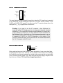
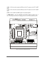
Figure 1: CPU board layout and default jumper settings
8 7 6 5 4 3 2 1
O
O
N
N

These jumpers come in the SHORT position as a default factory setting:
J2: The CPU is connected to the +5V power supply through this jumper
J3: The CPU AVCC supply pin is connected +5V power supply through this jumper
J4: The CPU AGND supply pin is connected to the GND through this jumper
J5: The CPU AVR+ pin is connected to the +5V voltage through this jumper
J6: The CPU AVR- pin is connected to the 0V voltage through this jumper
J7-9: The CPU UART1 signals are connected to the K7 connector
J13: The board is powered from the +5V from the power supply voltage regulator
J19: The CPU HRQ pin is connected to the SDA Mainboard signal
J20: The CPU #HAK pin is connected to the SCL Mainboard signal

CPU board does not come with power supply, please check, if your
power supply match the requirements before you plug it to the CPU
board!
Power supply voltage:
9V
Power supply current (CPU board MB90F543 with Main board connected):
Single chip CPU mode, no external peripheral connected: 290mA max.
External bus mode, no peripheral connected: 350mA
External bus with:
keyboard connected: 450mA typical, but can vary with the keyboard used
(most of modern AT keyboard uses max. 100mA. User should check his
keyboard current requirements before connecting the keyboard to the
DevKit16 Mainboard).
keyboard and VGA interface connected: 650mA
Warning: If the DevKit16 is powered using the on-board stabilizer, the
supply current must not exceed the 1A limit of the stabilizer. Before
connecting any peripheral to the DevKit16, please check that its power
supply current requirements doesn’t does not cause this limit to be exceeded.

To the maximum extent permitted by applicable law, Fujitsu Microelectronics Europe GmbH
restricts its warranties and its liability for the DEVKIT16 and all its deliverables (eg. software,
application examples, target boards, evaluation boards, etc.), its performance and any consequential
damages, on the use of the Product in accordance with (i) the terms of the License Agreement and the
Sale and Purchase Agreement under which agreements the Product has been delivered, (ii) the
technical descriptions and (iii) all accompanying written materials. In addition, to the maximum extent
permitted by applicable law, Fujitsu Microelectronics Europe GmbH disclaims all warranties and
liabilities for the performance of the Product and any consequential damages in cases of unauthorised
decompiling and/or reverse engineering and/or disassembling. Note, the DEVKIT16 and all its
deliverables are intended and must only be used in an evaluation laboratory environment.
1. Fujitsu Microelectronics Europe GmbH warrants that the Product will perform substantially in
accordance with the accompanying written materials for a period of 90 days form the date of receipt
by the customer. Concerning the hardware components of the Product, Fujitsu Microelectronics
Europe GmbH warrants that the Product will be free from defects in material and workmanship
under use and service as specified in the accompanying written materials for a duration of 1 year
from the date of receipt by the customer.
2. Should a Product turn out to be defect, Fujitsu Microelectronics Europe GmbH´s entire liability and
the customer´s exclusive remedy shall be, at Fujitsu Microelectronics Europe GmbH´s sole
discretion, either return of the purchase price and the license fee, or replacement of the Product or
parts thereof, if the Product is returned to Fujitsu Microelectronics Europe GmbH in original
packing and without further defects resulting from the customer´s use or the transport. However,
this warranty is excluded if the defect has resulted from an accident not attributable to Fujitsu
Microelectronics Europe GmbH, or abuse or misapplication attributable to the customer or any
other third party not relating to Fujitsu Microelectronics Europe GmbH.
3. To the maximum extent permitted by applicable law Fujitsu Microelectronics Europe GmbH
disclaims all other warranties, whether expressed or implied, in particular, but not limited to,
warranties of merchantability and fitness for a particular purpose for which the Product is not
designated.
4. To the maximum extent permitted by applicable law, Fujitsu Microelectronics Europe GmbH´s and
its suppliers´ liability is restricted to intention and gross negligence.
NO LIABILITY FOR CONSEQUENTIAL DAMAGES
To the maximum extent permitted by applicable law, in no event shall Fujitsu
Microelectronics Europe GmbH and its suppliers be liable for any damages whatsoever
(including but without limitation, consequential and/or indirect damages for personal injury,
assets of substantial value, loss of profits, interruption of business operation, loss of information,
or any other monetary or pecuniary loss) arising from the use of the Product.
Should one of the above stipulations be or become invalid and/or unenforceable, the remaining
stipulations shall stay in full effect.

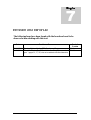
The following bugs have been found with the board and need to be
observed when working with this tool:
Date Revisions - Errors Revised
Version
05.11.1999 Version 1.2 is valid for CPU Board ver. 1.3 V1.2
13.02.2000 The table “Device Bus (K2) and Interface Bus (K1 ) connectors
pins” (pages 16, 17, 18) was not consistent with the schematics.
V1.21
Table1: List of found errors and revisions for version V1.2

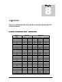
Here you will find Interface bus and Device Bus description and CPU
board schematics.
DIN Conn.
PIN
Device Bus Interface Bus
PIN NO. CPU Pin Nr. Function CPU PIN Nr. SIGNAL 2nd Function
A1 18 SOT0 85 AD00 P00
B1 19 SCK0 86 AD01 P01
C1 20 SIN0 87 AD02 P02
A2 24 SOT1 88 AD03 P03
B2 22 SCK1 89 AD04 P04
C2 21 SIN1 90 AD05 P05
A3 91 AD06 P06
B3 92 AD07 P07
C3 93 AD08 P10
A4 69 INT0 94 AD09 P11
B4 70 INT1 95 AD10 P12
C4 71 INT2 96 AD11 P13
A5 72 INT3 97 AD12 P14
B5 29 INT4 98 AD13 P15
C5 30 INT5 99 AD14 P16
A6 31 INT6 100 AD15 P17
B6 32 INT7 1 A16 P20
C6 25 SOT2 2 A17 P21
A7 26 SCK2 3 A18 P22
B7 28 SIN2 4 A19 P23
C7 5 A20 P24
A8 6 A21 P25
B8 7 A22 P26
C8 8 A23 P27
A9 9 ALE P30
B9 10 \RD P31
C9 12 \WRL P32
A10 13 \WRH P33
B10 14 HRQ P34

DIN Conn.
PIN
Device Bus Interface Bus
PIN NO. CPU Pin Nr. Function CPU PIN Nr. SIGNAL 2nd Function
C10 15 \HAK P35
A11 47 TIN0 16 RDY P36
B11 48 TOT0 17 CLK P37
C11 GND GND GND
A12 67 TIN1 18 SOT0 P40
B12 68 TOT1 19 SCK0 P41
C12 20 SIN0 P42
A13 24 SOT1 P45
B13 53 IN0 22 SCK1 P44
C13 54 IN1 21 SIN1 P43
A14 55 IN2 25 SOT2 P46
B14 56 IN3 26 SCK2 P47
C14 57 IN4 28 SIN2 P50
A15 58 IN5 SDA
B15 59 OUT2/IN6 SCL
C15 60 OUT3/IN7 61 PPG0 P80
A16 65 OUT0 62 PPG1 P81
B16 66 OUT1 67 TIN1 P86
C16 VCC VCC
A17 59 OUT3/IN7 33 ADTG P55
C17 60 OUT2/IN6 68 TOT1 P87
C17 AVCC 34 AVCC
A18 35 AVR+
B18 36 AVR-
C18 AGND 37 AGND
A19 38 AN0 P60
B19 39 AN1 P61
C19 GND GND GND
C20 40 AN2 P62
A21 41 AN3 P63
C20 43 AN4 P64
A21 44 AN5 P65
B21 45 AN6 P66
C21 46 AN7 P67
A22 61 PPG0 77 \RST
B22 62 PPG1 52 \HST
C22 63 PPG2 69 INT0 P90
A23 64 PPG3 70 INT1 P91
B23 71 INT2 P92
C23 72 INT3 P93
A24 73 TX0 29 INT4 P51
B24 74 RX0 30 INT5 P52
C24 75 TX1 31 INT6 P53
A25 76 RX1 32 INT7 P54
B25 53 IN0 P70
C25 54 IN1 P71
A26 55 IN2 P72
B26 56 IN3 P73
C26 59 OUT2/IN6 P76
A27 60 OUT3/IN7 P77
B27 NC(SGO)
C27 NC(SGA)

DIN Conn.
PIN
Device Bus Interface Bus
PIN NO. CPU Pin Nr. Function CPU PIN Nr. SIGNAL 2nd Function
A28 73 TX0 P94
B28 74 RX0 P95
C28 75 TX1 P96
A29 76 RX1 P97
B29 79 X1AJ
C29 80 X0AJ
A30 82 X0J
B30 83 X1J
C30 VCC VCC
A31 49 MD0
B31 50 MD1
C31 NC
A32 51 MD2
B32 NC
C32 GND GND
Page is loading ...
-
 1
1
-
 2
2
-
 3
3
-
 4
4
-
 5
5
-
 6
6
-
 7
7
-
 8
8
-
 9
9
-
 10
10
-
 11
11
-
 12
12
-
 13
13
-
 14
14
-
 15
15
-
 16
16
-
 17
17
-
 18
18
-
 19
19
-
 20
20
-
 21
21


Ask a question and I''ll find the answer in the document
Finding information in a document is now easier with AI
Related papers
-
Fujitsu FMC-16LX/FR User manual
-
-
-
-
-
-
-
-
-
Other documents
-
Siruba ASC-TBH100A Owner's manual
-
Philips 50PFL6870/V7 User manual
-
Crystorama ELS-7100-GA User manual
-
 urban ambiance UHP2326 Installation guide
-
 DAEWOO ELECTRONICS DSC-3210EGB User manual
-
Protocol 5872-3EA Tow Truck 3D Puzzle User manual
-
-
Acroprint ATR120 Quick start guide
-
Trend AD05-24 Product information
-
 AIMPIRE USB Desktop DAC Decoder DSD - Mini Audio Amplifier Decoder Aimpire DAC, DSD256 PCM44.1-384kHz/32bit, Thesycon Driver XMOS XU208 ES9018K2M OPA2134 Replaceable OP for DIY User manual


