Page is loading ...

Fujitsu Microelectronics Europe
User Guide
FMEMCU-UG-960014-10
MB96300 SERIES
EVALUATION BOARD
SK-96370-144PMC-GDC
USER GUIDE

SK-96370-144PMC-GDC User Guide
Revision History
FMEMCU-UG-960014-10 - 2 - © Fujitsu Microelectronics Europe GmbH
Revision History
Date Issue
20.05.2008 V1.0, HWe, First Release
This document contains 42 pages.

SK-96370-144PMC-GDC User Guide
Warranty and Disclaimer
© Fujitsu Microelectronics Europe GmbH - 3 - FMEMCU-UG-960014-10
Warranty and Disclaimer
To the maximum extent permitted by applicable law, Fujitsu Microelectronics Europe GmbH restricts
its warranties and its liability for the SK-96370-144PMC-GDC Board and all its deliverables (e.g.
software include or header files, application examples, target boards, evaluation boards, engineering
samples of IC’s etc.), its performance and any consequential damages, on the use of the Product in
accordance with (i) the terms of the License Agreement and the Sale and Purchase Agreement under
which agreements the Product has been delivered, (ii) the technical descriptions and (iii) all
accompanying written materials. In addition, to the maximum extent permitted by applicable law,
F
ujitsu Microelectronics Europe GmbH disclaims all warranties and liabilities for the performance of
the Product and any consequential damages in cases of unauthorized decompiling and/or reverse
engineering and/or disassembling. Note, the SK-96370-144PMC-GDC Board and all its
deliverables are intended and must only be used in an evaluation laboratory environment.
1. Fujitsu Microelectronics Europe GmbH warrants that the Product will perform substantially in
accordance with the accompanying written materials for a period of 90 days form the date of
receipt by the customer. Concerning the hardware components of the Product, Fujitsu
Microelectronics Europe GmbH warrants that the Product will be free from defects in material
and workmanship under use and service as specified in the accompanying written materials
for a duration of 1 year from the date of receipt by the customer.
2. Should a Product turn out to be defect, Fujitsu Microelectronics Europe GmbH´s entire liability
and the customer’s exclusive remedy shall be, at Fujitsu Microelectronics Europe GmbH´s
sole discretion, either return of the purchase price and the license fee, or replacement of the
Product or parts thereof, if the Product is returned to Fujitsu Microelectronics Europe GmbH in
original packing and without further defects resulting from the customer’s use or the transport.
However, this warranty is excluded if the defect has resulted from an accident not attributable
to Fujitsu Microelectronics Europe GmbH, or abuse or misapplication attributable to the
customer or any other third party not relating to Fujitsu Microelectronics Europe GmbH.
3. To the maximum extent permitted by applicable law Fujitsu Microelectronics Europe GmbH
disclaims all other warranties, whether expressed or implied, in particular, but not limited to,
warranties of merchantability and fitness for a particular purpose for which the Product is not
designated.
4. To the maximum extent permitted by applicable law, Fujitsu Microelectronics Europe GmbH´s
and its supplier’s liability are restricted to intention and gross negligence.
NO LIABILITY FOR CONSEQUENTIAL DAMAGES
To the maximum extent permitted by applicable law, in no event shall Fujitsu
Microelectronics Europe GmbH and its suppliers be liable for any damages whatsoever
(including but without limitation, consequential and/or indirect damages for personal
injury, assets of substantial value, loss of profits, interruption of business operation,
loss of information, or any other monetary or pecuniary loss) arising from the use of
the Product.
Should one of the above stipulations be or become invalid and/or unenforceable, the remaining
stipulations shall stay in full effect

SK-96370-144PMC-GDC User Guide
Contents
FMEMCU-UG-960014-10 - 4 - © Fujitsu Microelectronics Europe GmbH
0 Contents
REVISION HISTORY............................................................................................................ 2
WARRANTY AND DISCLAIMER ......................................................................................... 3
0 CONTENTS...................................................................................................................... 4
1 OVERVIEW...................................................................................................................... 6
1.1 Abstract................................................................................................................... 6
1.2 Features.................................................................................................................. 7
1.3 General Description................................................................................................. 8
2 INSTALLATION ............................................................................................................. 10
2.1 Connection/Power-On ........................................................................................... 10
2.2 Default Jumper settings for MB96370 Series......................................................... 11
2.3 Jumper Location.................................................................................................... 13
3 JUMPERS AND SWITCHES.......................................................................................... 14
3.1 Operating Mode (S1)............................................................................................. 14
3.2 Power Supply (S2, JP: 8, 15, 16, 17, 22)............................................................... 15
3.3 Subclock (JP: 1, 2) ................................................................................................ 16
3.4 Analog Power Supply Voltage (JP: 11, 12, 13, 14) ................................................ 17
3.5 Alarm Comparator (JP: 85).................................................................................... 17
3.6 Reset Generation (JP: 33, 41, 46, 47, 48) ............................................................. 18
3.7 User Buttons SW1, SW2, SW3, SW4, SW5, SW6 (JP: 3, 4, 5, 6, 7)...................... 19
3.8 I
2
C pull-up resistor (JP: 9, 10)................................................................................ 19
3.9 LIN / UART............................................................................................................ 20
3.10 CAN interfaces (JP: 24, 26, 34, 35) ....................................................................... 21
3.11 External Flash memory (JP: 49, 52, 56) ................................................................ 22
3.12 External SRAM memory (JP: 50, 53, 59)............................................................... 22
3.13 Graphic Display Controller interface (JP: 54, 55, 56, 57, 58, 60, 85, 86)................ 23
4 CONNECTORS.............................................................................................................. 24
4.1 Power connector (X7)............................................................................................ 24
4.2 MCU pin header connectors (X20A, X20B, X21, X22 and X23)............................. 24
4.3 LIN-UART connectors (X5, X9) ............................................................................. 24
4.4 CAN Connector (X6, X8) ....................................................................................... 25
4.5 USER-LEDs & optional LC-Display (J1) ................................................................ 26
4.6 In-Circuit-Programming Connector (X4) ................................................................ 27
4.7 Alarm Comparator Connector (J2)......................................................................... 28
4.8 External Supply Voltage Vin (J3)........................................................................... 28

SK-96370-144PMC-GDC User Guide
Contents
© Fujitsu Microelectronics Europe GmbH - 5 - FMEMCU-UG-960014-10
4.9 Vcc 5 Volts (J4) ..................................................................................................... 28
4.10 Vcc 3.3 Volts (J5) .................................................................................................. 28
4.11 Vcc 2.5 Volts (J9) .................................................................................................. 28
4.12 Vcc 1.8 Volts (J10) ................................................................................................ 28
4.13 LIN Bus Inhibit (J6)................................................................................................ 28
4.14 LIN Bus Inhibit (J11).............................................................................................. 28
4.15 VCC Connector (J7) .............................................................................................. 28
4.16 GND Connector (J8).............................................................................................. 28
5 PROGRAMMING THE INTERNAL FLASH MEMORY................................................... 29
5.1 Asynchronous Mode.............................................................................................. 29
5.2 Synchronous Mode ............................................................................................... 31
6 APPENDIX..................................................................................................................... 32
6.1 Related Products................................................................................................... 32
7 INFORMATION IN THE WWW....................................................................................... 33
8 CHINA-ROHS REGULATION ........................................................................................ 34
9 RECYCLING .................................................................................................................. 36

SK-96370-144PMC-GDC User Guide
Chapter 1 Overview
FMEMCU-UG-960014-10 - 6 - © Fujitsu Microelectronics Europe GmbH
1 Overview
1.1 Abstract
The SK-96370-144PMC-GDC is a multifunctional evaluation board for the Fujitsu 16FX
Flash microcontroller MB96370 Series.
It can be used stand-alone for software development and testing or as a simple target board
to work with the emulator system.
The board allows the designer immediately to start software development before his own
final target system is available.

SK-96370-144PMC-GDC User Guide
Chapter 1 Overview
© Fujitsu Microelectronics Europe GmbH - 7 - FMEMCU-UG-960014-10
1.2 Features
< Supports Fujitsu’s 16FX MB96370 Series with 144 pin PMC / M08 package
or the MB2198 Emulator System with the Probe Cable MB2198-507-E.
< 9-15V unregulated external DC power supply
< On-board 3.3V switching mode voltage regulator
< Power-LEDs for all supply voltages
< Onboard voltage supervisor monitor
< In-Circuit serial Flash programming (UART0 or UART2)
< All resources available for evaluation
< All MCU pins routed to connectors
< 4 MHz main crystal
< 32 kHz crystal for sub clock operation
< Two RS232- or LIN interfaces
< Two CAN interfaces
< 3 V capable CAN, LIN, and RS232 transceivers
< 8 User LEDs
< Optional: alphanumeric standard LC-Display connectable instead of LEDs
< Reset button, Reset LED
< 5 User buttons
< 8 MByte FLASH
< 2 MByte SRAM
< Connector for Fujitsu Graphic-Controller boards (e.g.: CREMSON-STARTERKITLIME)
< External bus interface routed to 96 pin and 48 pin DIN 41612 (VG) connectors
< Power Supply: 5V, 3.3V, 2.5V and 1.8V
This board must only be used for test applications
in an evaluation laboratory environment.

SK-96370-144PMC-GDC User Guide
Chapter 1 Overview
FMEMCU-UG-960014-10 - 8 - © Fujitsu Microelectronics Europe GmbH
1.3 General Description
The SK-96370-144PMC-GDC supports the F
2
MC-16FX microcontrollers of MB96370 Series
with LQFP144-M08 (PMC) package.
It can be used as a stand-alone evaluation board or as a target board for the emulator
debugger.
1.3.1 MCU Clocks
The board is supplied with a socketed 4 MHz crystal as main oscillation source. Using the
internal PLL of the IC, internal clock rates up to 56 MHz can be achieved.
1.3.2 RS-232 and LIN
Two separate RS232 transceivers and two single-wire LIN-transceivers (TLE7259) are
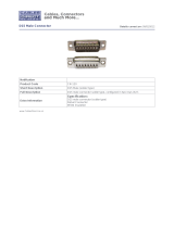
available to connect two out of three on-chip UARTs to 9-pin D-Sub connectors (X5, X9).
The transceivers generate the adequate RS232 levels for the receive (RXD) and transmit
(TXD) and LIN bus lines. In RS232 mode, either the DTR line or the RTS line can be
selected with jumpers (JP23 and JP38) to generate a system reset. The RTS signal can be
shortcut to CTS using the jumpers JP19 and JP36. Each of the four D-Sub connectors can
be configured as RS232 or LIN. The LIN Vs line can be powered by the unregulated supply
input of the board, so no additional supply is needed (JP28 and JP42).
All transceivers are fully 3.3V IO compatible to enable low voltage applications.
In-circuit programming (asynchronous) can be done via LIN-UART 0 and 2 (X5, X9).
1.3.3 CAN Bus
Two high-speed CAN transceivers (TLE6250GV33) can be connected to the CAN interfaces
of the MCU to allow easy connection to CAN networks.
All transceivers are fully 3.3V IO compatible to enable low voltage applications.
1.3.4 MCU Pins
All pins of the microcontroller except the oscillator pins X0/X1 and X0A/X1A are connected
to edge connectors and are directly available to the user.
1.3.5 Power Supply
The on-board switching mode voltage regulators allow the user to connect an unregulated
DC input voltage of +9V to +15V, and supplies all voltages needed by the board and an
optional graphic sub-board. The regulators are rated with 3A (5V and 3.3V) resp. 1.5A (2.5V,
1.8V) and are thermally protected against overload.
1.3.6 User Buttons
There are six push button switches on the board, which can be connected to input ports of
the microcontroller. This allows the user to evaluate external Interrupts, external timer trigger
or Input Capture functions as well as simple input polling. One button is reserved as ‘Reset’-
button for the microcontroller, controlled by the supply monitor IC.
1.3.7 User LEDs and optional LCD
Eight user LEDs are connected to Port 09 and grounded by two 1k resistor networks (RN1,
RN2). If these LEDs are not required, these resistor networks can be removed to disconnect
the LEDs and to free the I/O port.

SK-96370-144PMC-GDC User Guide
Chapter 1 Overview
© Fujitsu Microelectronics Europe GmbH - 9 - FMEMCU-UG-960014-10
1.3.8 I2C Bus
Additional 10 kOhm pull-up resistors can be connected to the I²C bus lines by setting the
according jumpers. JP9 is for SDA0 and JP10 for SCL0.
1.3.9 Emulator System
If the board is used as an emulator target board, the microcontroller must be removed from
the socket and the corresponding probe cable has to be mounted:
Table 1-1: Emulation System
Series V-Chip Probe cable Socket
MB96370 MB96V300B
MB2198-507-E
NQPACK144SD-ND
HQPACK144SD

SK-96370-144PMC-GDC User Guide
Chapter 2 Installation
FMEMCU-UG-960014-10 - 10 - © Fujitsu Microelectronics Europe GmbH
2 Installation
2.1 Connection/Power-On
Carefully remove the board from the shipping carton.
First, check if there are any damages before powering up the evaluation board.
For the power supply a DC input voltage of 9V – 15V is recommended. The positive
voltage (+) must be connected to the center pin, and ground (GND) must be
connected to the shield of the connector X7!
After power-on (Switch S2 or JP22), the red power-on LEDs (LD9, LD10, LD11, and LD12)
should be lit. If the LEDs do not light up, switch off the power supply and check input polarity
and current capability of the DC supply used. Please do not look directly into the LEDs to
prevent harming your eyes.
The in-circuit programming allows the user to program own applications into the Flash
memory. The procedures for Flash programming are described in chapter 5.
If the board shall be used as an emulator target board, switch off the power supply and
remove the microcontroller from the socket. Now the probe cable can be mounted on the
socket. Take care of the pin 1 marking on the socket and fasten the probe cable with the
provided screws.
Do not use any other probe cable than MB2198-507-E only!
Connect the probe cable to the MB2198-500 emulation Adapter Board. Check all jumper
settings of the evaluation board, the Probe Cable, and the Adapter Board.
When turning on the system, be sure to use the following power-up sequence:
1. Power up the Emulator Main Unit (MB2198-01)
2. Power up the Adapter Board (MB2198-500), if needed
3. Power up the target Board (SK-96370-144PMC-GDC)
To turn off the system, switch off the components in reverse order, beginning with the target
Board.
Please refer to the corresponding user manuals and application notes for the emulator how
to set up the emulator system. After power on the ‘UVCC’-LED of the emulator must be on.
Note:
Some customers experience connectivity problems when connecting the MCU into
the socket adapter. Only the small red screwdriver available in your box should be
used to connect the cover (HQPACK) onto the socket (NQPACK).
If the four screws are not tightening equally, then it may cause a poor contact.
Do not screw the cover too tight (max 0.054 Nm). If you have connectivity problems
then please loosen the screws and tighten again the screws equally.
Do not clean NQPACK, YQPACK, and YQSOCKET with steam. Cleaning material will
contaminate inside of connector.

SK-96370-144PMC-GDC User Guide
Chapter 2 Installation
© Fujitsu Microelectronics Europe GmbH - 11 - FMEMCU-UG-960014-10
2.2 Default Jumper settings for MB96370 Series
The following table lists all jumpers including its default setting and location on the starterkit.
Jumper Description / Function Type
Default
Setting
Coordinates
JP1 X1A Jumper 3 pin 1-2 J 10
JP2 X0A Jumper 4 pin 1-2 J 10
JP3 Switch SW1 : INT0/NMI Jumper 2 pin Closed G 6
JP4 Switch SW2 : INT5 Jumper 2 pin Closed G 6
JP5 Switch SW3 : TIN1 Jumper 2 pin Closed H 6
JP6 Switch SW4 : IN0 / TTG4/0 Jumper 2 pin Closed H 6
JP7 Switch SW5 : IN1 / TTG5/1 Jumper 2 pin Closed H 6
JP8 C pin Jumper 2 pin Closed I 14
JP9 SDA0 pull-up Jumper 2 pin Open G 15
JP10 SCL0 pull-up Jumper 2 pin Open G 15
JP11 AVCC Jumper 2 pin Closed J 16
JP12 AVRH Jumper 2 pin Closed J 15
JP13 AVRL Jumper 2 pin Closed J 15
JP14 AVSS Jumper 2 pin Closed K 15
JP15
Voltage selection for MCUVCC
(3.3V only for SK-96370-144PMC-GDC with extern. memory)
Jumper 3 pin
2-3
Do not change!
J 17
JP16 MCUVCC Jumper 2 pin Closed K 17
JP17 DVCC Jumper 3 pin 2-3 L 12
JP18 DVSS Jumper 2 pin Closed L 10
JP19 UART0 : CTS / RTS Jumper 2 pin Closed I 3
JP20 CAN0 Transceiver type Solder JP 3 pin 1-2 D 4
JP21 SIN0 : RS232 / LIN transceiver Jumper 3 pin 1-2 H 5
JP22 Mains Switch Jumper 2 pin Open L 17
JP23 UART0 : DTR / RTS Jumper 3 pin Open H 3
JP24 CAN0 RxD Jumper 2 pin Closed D 4
JP25 SOT0 : RS232 / LIN transceiver Jumper 3 pin 1-2 I 5
JP26 CAN0 TxD Jumper 2 pin Closed D 3
JP27 UART0 : RS232 / LIN Jumper 3 pin 1-2 I 3
JP28 UART0 : LIN VBat Jumper 2 pin Open H 3
JP29 UART0 : LIN-Enable Jumper 2 pin Open I 3
JP30 LIN0 Transceiver type Solder JP 3 pin 1-2 I 5
JP31 UART0 : LIN Master Jumper 2 pin Open J 3
JP32 CAN1 Transceiver type Solder JP 3 pin 1-2 G 4
JP33 Reset by UART 0 / 2 Jumper 3 pin Open J 5
JP34 CAN1 RxD Jumper 2 pin Closed G 4
JP35 CAN1 TxD Jumper 2 pin Closed G 3
JP36 UART2 : CTS / RTS Jumper 2 pin Closed K 3
JP37 SIN2 : RS232 / LIN Jumper 3 pin 1-2 K 5
JP38 UART2 : DTR / RTS Jumper 3 pin Open K 3
JP39 SOT2 : RS232 / LIN Jumper 3 pin 1-2 K 5
JP40 UART2 : RS232 / LIN Jumper 3 pin 1-2 K 3
JP41 UART Reset / Inverter Jumper 3 pin Open J 7

SK-96370-144PMC-GDC User Guide
Chapter 2 Installation
FMEMCU-UG-960014-10 - 12 - © Fujitsu Microelectronics Europe GmbH
Jumper Description / Function Type
Default
Setting
Coordinates
JP42 UART2 : LIN VBat Jumper 2 pin Open K 3
JP43 UART2 : LIN-Enable Jumper 2 pin Open L 3
JP44 LIN2 Transceiver type Solder JP 3 pin 1-2 L 5
JP45 UART2 : LIN Master Jumper 2 pin Open M 3
JP46 Direct Reset / Delayed Solder JP 3 pin 1-2 J 7
JP47 Voltage Monitor Solder JP 3 pin 2-3 J 8
JP48 MCU Reset Jumper 2 pin Closed J 8
JP49 FLASH : Word / Byte access Jumper 3 pin 1-2 D 13
JP50 SRAM : Word / Byte access Jumper 3 pin 1-2 F 13
JP52 FLASH : 16-bit / 8-bit interface Jumper 3 pin 1-2 D 13
JP53 SRAM : 16-bit / 8-bit interface Jumper 3 pin 1-2 F 13
JP54 Set A24 to GND for GDC interface Solder JP 2 pin Closed C 15
JP55 Set A25 to GND for GDC interface Solder JP 2 pin Closed C 16
JP56 FLASH / LIME Jumper 4 pin 2-4 E 14
JP57 Select CS3/CS2 for GDC interface Jumper 2 pin Open E 14
JP58 Supply 1V8 to GDC interface Solder JP 2 pin Closed C 4
JP59 SRAM Jumper 3 pin 2-3 E 13
JP60 External Vin Solder JP 2 pin Open C 8
JP70 Manual GDC reset (GLRST) Solder JP 2 pin Closed C 7
JP71 Manual GDC reset (FLRST) Solder JP 2 pin Closed C 7
JP85 ALARM0 Jumper 2 pin Closed L 15
Table 2-1: Jumper Settings

SK-96370-144PMC-GDC User Guide
Chapter 2 Installation
© Fujitsu Microelectronics Europe GmbH - 13 - FMEMCU-UG-960014-10
2.3 Jumper Location
The following picture shows the silk plot of the starter-kit with marked default jumper
settings.
A B C D E F G H I J K L M
1 1
2 2
3 3
4 4
5 5
6 6
7 7
8 8
9 9
10 10
11 11
12 12
13 13
14 14
15 15
16 16
17 17
18 18
19 19
20 20
A B C D E F G H I J K L M
Figure 2-1: Default Jumper Settings

SK-96370-144PMC-GDC User Guide
Chapter 3 Jumpers and Switches
FMEMCU-UG-960014-10 - 14 - © Fujitsu Microelectronics Europe GmbH
ON
OFF
DIP-Switch S1
(RUN Mode)
MD0 MD1 MD2 nc
1 2 3 4
ON
OFF
DIP-Switch S1
(Programming Mode)
MD0 MD1 MD2 nc
1 2 3 4
3 Jumpers and Switches
This chapter describes all jumpers and switches that can be modified on the evaluation
board. The default setting is shown with a grey shaded area.
3.1 Operating Mode (S1)
This switch controls the MCU operation mode after Reset.
Please take care of the following mode settings:
DIP switch Setting Logical value
ON (closed) 1 (high)
S1-1
(MD0)
OFF (open) 0 (low)
ON (closed) 1 (high)
S1-2
(MD1)
OFF (open) 0 (low)
ON (closed) 1 (high)
S1-3
(MD2)
OFF (open) 0 (low)
ON (closed) Not connected
S1-4
(Not used)
OFF (open) Not connected
Table 3-1: MCU Operating Mode
Figure 3-1: MCU mode switch: RUN mode (Fixed Vector Mode)
Figure 3-2: MCU mode switch: Flash Programming mode

SK-96370-144PMC-GDC User Guide
Chapter 3 Jumpers and Switches
© Fujitsu Microelectronics Europe GmbH - 15 - FMEMCU-UG-960014-10
3.2 Power Supply (S2, JP: 8, 15, 16, 17, 22)
The on-board voltage regulator provides stabilized 5V
*
1
and 3.3V supplies to the MCU
*
1
and
peripherals. Even though they are thermally protected against overload, care must be taken
when supplying current for additional circuitry.
The LIN Vs line can be connected directly to the input supply of the board by jumpers. In this
case, the input voltage to the board has to be suitable for the connected bus devices (mostly
around 12V). Since there is a protection diode between Vin and Vs, it is not possible to
power the board over the LIN bus.
S2 Power Switch
JP8 Core power supply stabilization capacitor
JP15 Selects the power supply voltage for the microcontroller
For SK-96370-144PMC-GDC use only 3.3V, because of the external memory
JP16 Connects the power supply voltage to the microcontroller. An ampere meter can be
used instead for power consumption measurement.
JP17 Selects the Stepper Motor Driver Voltage (3.3V or 5V)
JP22 Jumper to override the power switch S2
Jumper Setting Description
Closed An external capacitor is connected
JP8
(C-pin)
Open An external capacitor is not connected
1 - 2
Power supply (VCC) for MCU is set to 5V
(Not allowed for SK-96370-144PMC-GDC)
JP15
*1
(MCUVCC)
2 - 3 Power supply (VCC) for MCU is set to 3V3
1 - 2 MCU is disconnected from VCC
JP16
(MCUVCC)
2 - 3 MCU is connected to VCC
1 - 2 SMC (DVCC) supply voltage is set to 5V
JP17
(DVCC)
2 - 3 SMC (DVCC) supply voltage is set to 3.3V
Closed Board is always switched on
JP22
(Mains)
Open Board power is controlled by switch S2
Table 3-2: Power Supply Configuration
By default, all Board supplies are set to 3.3V.
*1
For SK-96370-144PMC-GDC use only 3.3V, because of the external memory

SK-96370-144PMC-GDC User Guide
Chapter 3 Jumpers and Switches
FMEMCU-UG-960014-10 - 16 - © Fujitsu Microelectronics Europe GmbH
3.3 Subclock (JP: 1, 2)
Some devices like e.g. MB96F37xRW support a 32 kHz sub-clock (X0A, X1A), other devices
like e.g. MB96F37xRS do not support a sub-clock but will offer additional port-pins (e.g.
P04_0, P04_1) instead.
Please check the related datasheet.
JP1: defines usage of pin 69 (X1A)
JP2: defines usage of pin 68 (X0A)
Jumper Setting Description
1-4 Pin 68 is connected to the 32 kHz sub-clock (X0A)
2-4 Pin 68 is used as port pin P04_0
JP2
(X0A)
3-4
Pin 68 is connected to GND (in case that subclock-
device is used, but no 32 kHz crystal is connected)
1-2 Pin 69 is connected to the 32 kHz sub-clock (X1A)
JP1
(X1A)
2-3 Pin 69 is used as port pin P04_1
Default: JP1: 1-2, JP2: 1-4
By default, the 32 kHz sub-clock-crystal is connected to the microcontroller.
4
3
1
2
Pin
-
out JP2:

SK-96370-144PMC-GDC User Guide
Chapter 3 Jumpers and Switches
© Fujitsu Microelectronics Europe GmbH - 17 - FMEMCU-UG-960014-10
3.4 Analog Power Supply Voltage (JP: 11, 12, 13, 14)
The power supply as well as the positive reference voltage for the A/D-converter can be
provided internally or externally.
JP11, JP14 connects analog power supply voltages (AVcc and AVss)
JP12 connects the low pass filtered analog reference voltage AVRH to AVcc
JP13 connects the low pass filtered analog reference voltage AVRL to AVss
Jumper Setting Description
Closed AVcc is connected to Vcc
JP11
(AVcc)
Open AVcc is disconnected from Vcc
Closed AVRH is connected to AVcc
JP12
(AVRH)
Open AVRH defined by resistor network
*
1
Closed AVRL is connected to AVss
JP13
(AVRL)
Open AVRL defined by resistor network
*1
Closed AVss is connected to GND
JP14
(AVss)
Open AVss is disconnected from GND
*
1
By default the resistor network (R16, R17, R20, R21) is not mounted on the board
Table 3-3: ADC Supply
Default: JP11, JP12, JP13, and JP14 are closed
By default, the A/D-converter supply and reference voltage is the same as the
microcontroller supply voltage.
Note:
If JP11 and JP14 are open, the user has to supply an adequate analog voltage supply (AVcc
and AVss) to the A/D-converter.
If JP12 and JP13 are open, the resistors R16, R17, R20, and R21 define AVRH and AVRL.
By default the resistor network (R16, R17, R20, and R21) is not mounted on the board.
3.5 Alarm Comparator (JP: 85)
Potentiometer RP2 is connected to ALARM0 in order to evaluate comparator 0 of the
microcontroller. Any voltage between VCC and GND can be set. Additionally the adjusted
voltage can be measured at connector J2.
JP78 One potentiometer can be connected to the ALARM0/AN8
Jumper Setting Description
Closed Pin 26 (ALRAM0/AN8) of the MCU is connected to RP2
JP85
(ALARM0)
Open Pin 26 (ALRAM0/AN8) of the MCU is not connected
Table 3-4: Alarm Comparator

SK-96370-144PMC-GDC User Guide
Chapter 3 Jumpers and Switches
FMEMCU-UG-960014-10 - 18 - © Fujitsu Microelectronics Europe GmbH
3.6 Reset Generation (JP: 33, 41, 46, 47, 48)
In addition to the internal Power-On reset, the microcontroller can be reset by an external
reset circuit (Voltage Monitor) and also by a RS232 interface. Refer to the chapter ‘LIN /
UART Connectors (X5 or X9)’ for DTR / RTS selection.
JP33 Selects X5 or X9 as reset source.
JP41 The signal on the DTR/RTS line can be negated with this jumper.
Remove the jumper in order to disable the RS232 reset circuit.
JP46 Selects the mode of the reset button SW6.
JP47 A voltage supply monitor allows monitoring of 1V8 or 2V5 power supply.
JP48 Open this jumper if no external Reset shall be generated.
In this case only the internal reset is active (e.g.: power-on).
Jumper Setting Description
1-2 X5 (UART0) is used to generate Reset
JP33
(UART RESET)
2-3 X9 (UART2) is used to generate Reset
1-2 No polarity inversion for the DTR/RTS signal
JP41
(DTR / DTRx)
2-3 Polarity inversion for the DTR/RTS signal
1-2 Reset is applied immediately when SW6 is pressed
JP46
(Reset imm./delayed)
2-3 Reset is applied when SW6 is pressed > 2sec
1-2 The voltage supply monitor observes 1V8
JP47
(Monitor 1V8 / 2V5)
2-3 The voltage supply monitor observes 2V5
Closed External reset generation is active
JP48
(RST MCU)
Open No external reset generation
Table 3-5: Reset Connection
By default, the external reset is enabled and set to immediate reset while the reset by UART
is disabled.
Note:
While a reset signal is asserted the red Reset-LED LD13 is lit.
During normal operation, this LED should be off!
If JP41 (DTR/DTRx) is set, the UART RESET jumper (JP33) and the according DTR/RTS
(JP23 and JP38) jumper have to be set, too.
If the reset LED is steadily on, check the power supply input voltage and the settings for the
reset-generation by UART.

SK-96370-144PMC-GDC User Guide
Chapter 3 Jumpers and Switches
© Fujitsu Microelectronics Europe GmbH - 19 - FMEMCU-UG-960014-10
3.7 User Buttons SW1, SW2, SW3, SW4, SW5, SW6 (JP: 3, 4, 5, 6, 7)
Five user push buttons (SW1-SW5) can be connected to the microcontroller.
JP3, 4, 5, 6, 7 Each push button can be connected separately.
Jumper Setting Description
Closed Pin 139 (INT0/NMI) of the MCU is connected to “SW1”
JP3
(SW1)
Open No connection to the microcontroller
Closed Pin 19 (FRCK0) of the MCU is connected to “SW2”
JP4
(SW2)
Open No connection to the microcontroller
Closed Pin 22 (TIN1) of the MCU is connected to “SW3”
JP5
(SW3)
Open No connection to the microcontroller
Closed Pin 20 (IN0/TTG4/0) of the MCU is connected to “SW4”
JP6
(SW4)
Open No connection to the microcontroller
Closed Pin 21 (IN1/TTG5/1) of the MCU is connected to “SW5”
JP7
(SW5)
Open No connection to the microcontroller
Table 3-6: User Push Buttons
Default: JP3, 4, 5, 6, 7 closed
By default, all push-buttons are connected to the microcontroller.
3.8 I
2
C pull-up resistor (JP: 9, 10)
Two 10k pull-up resistors can be connected to the I
2
C signal line.
JP9, 10 10k pull-up resistors can be connected to SDA0 and SCL0
Jumper Setting Description
Closed A 10k pull-up resistor is connected to SDA0
JP9
(SDA0)
Open No pull-up resistor is connected to SDA0
Closed A 10k pull-up resistor is connected to SCL0
JP10
(SCL0)
Open No pull-up resistor is connected to SCL0

SK-96370-144PMC-GDC User Guide
Chapter 3 Jumpers and Switches
FMEMCU-UG-960014-10 - 20 - © Fujitsu Microelectronics Europe GmbH
3.9 LIN / UART
There are two identical circuit blocks for LIN or RS232 connections. Each of the two D-Sub
connectors can be configured as LIN or RS232 interface. DTS or RTS can be selected as
reset source, and RTS and CTS can be connected by a jumper, since some terminals and
Flash programming tools need this connection. Pin 1 (Vs) of X5 and X9 can be connected to
the voltage input of the board by jumpers in order to supply the LIN bus.
3.9.1 LIN-UART 0 (JP: 19, 21, 23, 25, 27, 28, 29, 31)
Jumper Setting Description
1-2 SIN0 is connected to RS232 transceiver
JP21
(RXD)
2-3 SIN0 is connected to LIN transceiver
1-2 SOT0 is connected to RS232 transceiver
JP25
(TXD)
2-3 SOT0 is connected to LIN transceiver
1-2 X5 pin 2 is connected to RS232 transceiver
JP27
(RS232/LIN)
2-3 X5 pin 2 is connected to LIN transceiver
Closed RTS and CTS of X5 are connected
JP19
(RTS-CTS)
Open RTS and CTS of X5 are not connected
1-2 DTR signal (pin 6 of X5) is used as reset source
JP23
(DTR/RTS)
2-3 RTS signal (pin 7 of X5) is used as reset source
Closed LIN transceiver is enabled
JP29
(LIN enable)
Open LIN transceiver is disabled
Closed LIN-UART0 is LIN Master
JP31
(LIN master)
Open LIN-UART0 is LIN Slave
Closed LIN bus (X5 pin 1) is powered by the board
JP28
(LIN Vbat)
Open LIN bus (X5 pin 1) is not powered by the board
Table 3-7: UART0 Settings
/