UM018606-0109 Schematics
Z8 Encore! XP
®
F082A Series Development Kit
User Manual
9
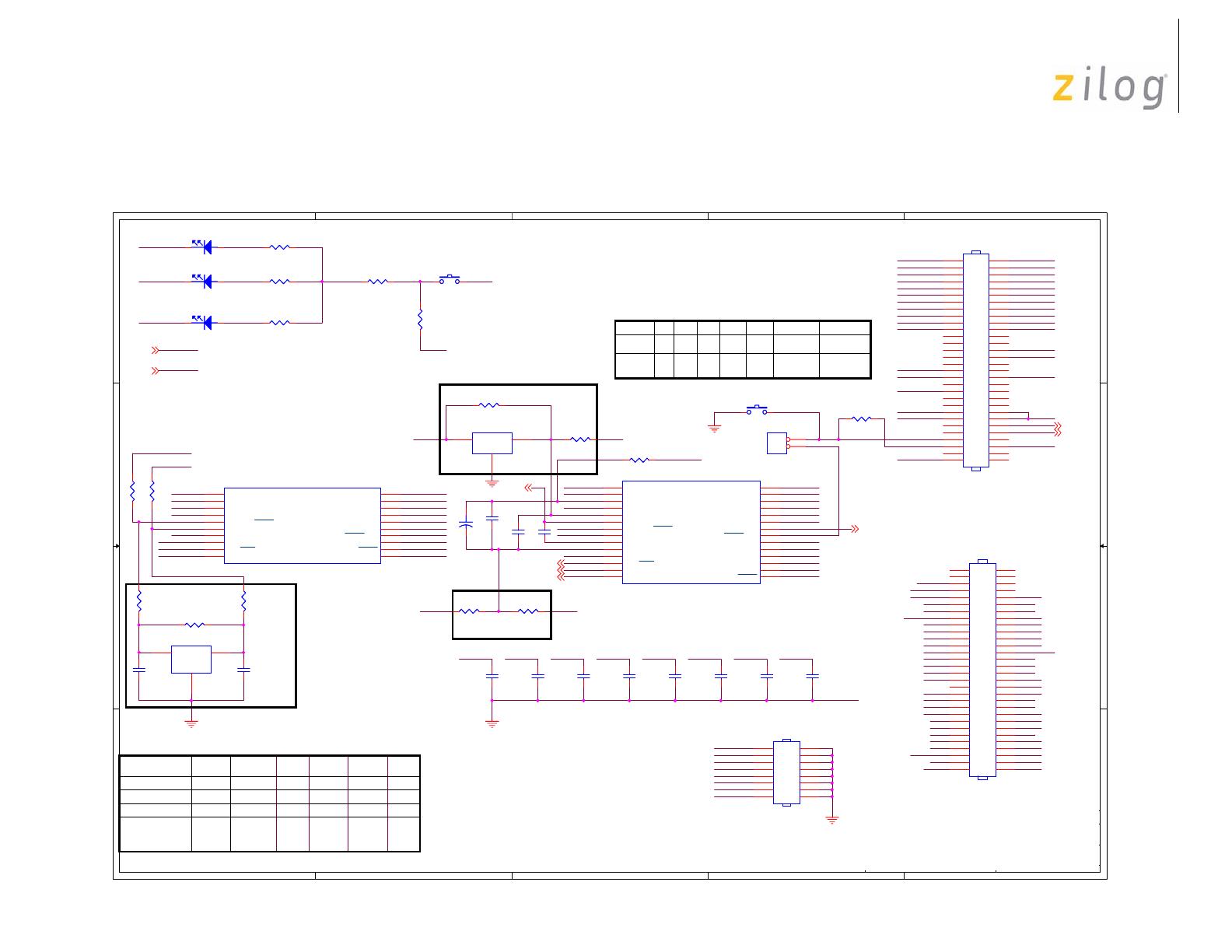
Schematics
Figure 3 and Figure 4 on page 10 display the schematics for Z8 Encore! XP F082A Series development board.
Figure 3. Schematic, Z8 Encore! XP
®
F082A Series MCU Development Board
5
5
4
4
3
3
2
2
1
1
D D
C C
B B
A A
PB0_ANA0 PB2_ANA2
VCC_33V
PB3_ANA3
GND
PB1_ANA1
PB3_ANA3
PB0_ANA0
PB4_ANA7
PB2_ANA2
A20
-CS0
A12
-IOREQ
-F91_WE
A13
GND
GND
A17
A21
VCC_33V
A14
D1
VCC_33V
D7
-DIS_FLASH
GND
A6 A0
D3
D6
-BUSACK
A3
D2
VCC_33V
A15
A4
-TRSTN
D0
-MREQ
A7
A10
A9
A16A18
A11
-INSTRD
A19
A5
GNDD5
-CS1
A22
A1A2
-CS2
-RD
A8
GND
D4
A23
-WR
-BUSREQ
GND
PB7
PA3_CTS0
PC7
VCC_33V
PC4
PA7_T1OUT PA2
PA1_T0OUT_JPGND
GND
PC5
PA4_RXD0 PA5_TXD0
GND
GND
PB6
PA0_T0IN_JP
PC6
PA6_nT1OUT
PA7_T1OUT
GNDVCC_33V
GND
-DIS_IrDA
PB1_ANA1
PA2
VCC_33V
GND
PA5_TXD0
PB1_ANA1 PB0_ANA0
DBG
PA3_CTS0
PA4_RXD0
PB2_ANA2
PB3_ANA3
PA0_T0IN
PC3_COUT
PA7_T1OUT
PC3_COUT
PC2_ANA6
PC1_ANA5
PC0_ANA4
PD0
PA6_nT1OUT
PC2_ANA6 PB4_ANA7
PC0_ANA4
PC1_ANA5
PC2_ANA6
PB6
PB7GND
PC5
PB2_ANA2
PA2
PC0_ANA4
PC2_ANA6
PA5_TXD0
PD0
PC3_COUT
PC1_ANA5
PA4_RXD0 PC4
VCC_33V
PC7
PA2
PA6_nT1OUT
PA1_T0OUT
PC6
PA3_CTS0
GND
PC1_ANA5
PA7_T1OUT
PB0_ANA0
GND
PA1_T0OUT
PB1_ANA1
PA0_T0IN
PB4_ANA7
PC0_ANA4
PB3_ANA3
DBG
PB4_ANA7 PC2_ANA6
PC0_ANA4
PB2_ANA2
PB0_ANA0
PC1_ANA5
PB3_ANA3
PB1_ANA1
PB5_JPPC3_COUT
PD0
GND
VCC_33V
VCC_33V
PA6_nT1OUT
-RESET
VCC_33V
PA0_T0IN_JP
PA1_T0OUT_JP
PB5
PB5_JP
GND
VCC_33V
DBG
-DIS_IRDA
-DIS_232
PA3_CTS0
PA4_RXD0
PA5_TXD0
SENSE
Title
Size Document Number Rev
Date: Sheet
of
96C0941-001 D
XP 4K MDS Processor Module. Schematic.
B
23Tuesday, March 18, 2008
Title
Size Document Number Rev
Date: Sheet
of
96C0941-001 D
XP 4K MDS Processor Module. Schematic.
B
23Tuesday, March 18, 2008
Title
Size Document Number Rev
Date: Sheet
of
96C0941-001 D
XP 4K MDS Processor Module. Schematic.
B
23Tuesday, March 18, 2008
connector 2
connector 1
for
reference
only
If Module is plugged onto the Dev Platform the local
RS232 interface is disabled by pin 50 of JP2
TEST
20 pin footprint
28 pin footprint
RESET/TEST2
Note 1:
PB6 and PB7 are dual function pins (GPIO or Analog supply)
R12, R13, R16, and R17 are zero-ohm resistors used in
conjunction with GPIO Control Registers to select function
desired. C21, C22, and C23 are bypass capacitors that are used
for better noise rejection. U8 is an optional filter that can
be used to improve the quality of the Analog Supply. The
development board is shipped configured for Analog Supply.
Table 1 shows the configurations recommended
NOTE 1:
NOTE 1:
NOTE 2
Note 2: The XP supports internal, external crystal, external
ceramic resonator, external R/C and external CMOS drive
clock modes. R14, R15, R18, C19, C20 and Y1 are used to
support the clock mode selected. The development board is
shipped configured for external 20MHz ceramic resonator or
internal clock operation. When using Internal oscilator,
pins 7 and 8 could be used as GPIO ports PA0 and PA1. To do
so install R20 and R21.
Table 2 shows the recommended clock mode configurations.
Clock Mode R14 R15 R18 C19 C20 Y1
Internal Only none none none none none none
Crystal 0 Ohm 0 Ohm none Yes Yes Yes
Ceramic Res 0 Ohm 0 Ohm none none none Yes
External CMOS none none none none none none
TABLE 2
(Use PA0_T0IN
pin on JP2)
Supply
R12 R13 R16 R17 R22 U8 C21...C23
Analog IN OUT IN OUT OUT optional IN
GPIO OUT IN OUT IN IN OUT OUT
TABLE 1
NOTE 3:
Resistors R20 and R21 are not populated. See Note 2.
C22
0.033uF
C22
0.033uF
R16
0
R16
0
R21
0
R21
0
R10
10
R10
10
R18
1M
R18
1M
C13
0.001uF
C13
0.001uF
R15
0
R15
0
R9
100K
R9
100K
R19
10K
R19
10K
D2
GREEN
D2
GREEN
21
SW1SW1
R22
0
R22
0
+
C23
30uF
+
C23
30uF
D3
YELL
D3
YELL
21
D4
RED
D4
RED
21
C17
0.001uF
C17
0.001uF
C21
0.033uF
C21
0.033uF
C11
0.001uF
C11
0.001uF
JP2
HEADER 30x2/SM
JP2
HEADER 30x2/SM
2
4
6
8
10
12
14
16
18
20
22
24
26
28
30
32
34
36
38
40
42
44
46
48
50
52
54
56
58
60
1
3
5
7
9
11
13
15
17
19
21
23
25
27
29
31
33
35
37
39
41
43
45
47
49
51
53
55
57
59
C16
0.001uF
C16
0.001uF
R17
0
R17
0
U5
Z8F04xA_28
U5
Z8F04xA_28
GND
9
PC4/LED
16
PA6/T1IN/T1OUT
15
PA5/TXD0
14
PA4/RXD0
13
PA3/CTS0
12
PB3/ANA3/CLKIN
4
PA0/T0IN/T0OUTXIN
7
VDD
6
PB1/ANA1
28
PB0/ANA0
27
PC1/ANA5/CINN/LED
24
PC2/ANA6/LED
25
PC3/COUT/LED
26
PC0/ANA4/CINP/LED
23
PB2/ANA2
1
PC6/LED
19
PC7/LED
20
PA2/DE
11
PB5/Vref
3
PB4/ANA7
2
PA7/T1OUT
18
PC5/LED
17
PB7(AGND)
10
PA1/T0OUT/XOUT
8
PB6(AVDD)
5
RESET/PD0
21
DBG
22
C14
0.001uF
C14
0.001uF
Y1
20 MHz
Y1
20 MHz
1
1
2
2
3
3
R12
0
R12
0
R7
100
R7
100
C15
0.001uF
C15
0.001uF
C19C19
R13
0
R13
0
J2
HEADER 8X2
J2
HEADER 8X2
2
4
6
8
10
12
14
16
1
3
5
7
9
11
13
15
R20
0
R20
0
R8
100
R8
100
U6
Z8F04xA
U6
Z8F04xA
PB2/ANA2
2
PA4/RXD0
10
PA3/CTS0
9
PA2/DE
8
PB3/CLKIN/ANA3
3
PA1/T0OUT/XOUT
6
PA0/T0IN/T0OUT/XIN/
5
PB0/ANA0
20
PB1/ANA1
1
PC1ANA5/CINN/LED
17
PC0/ANA4/CINP/LED
16
DBG
15
PA7/T1OUT
13
PA6/T1IN/T1OUT
12
PA5/TXD0
11
RESET/PD0
14
GND
7
VDD
4
PC3/COUT/LED
19
PC2/ANA6/LED
18
C12
0.001uF
C12
0.001uF
R14
0
R14
0
SW2SW2
C20C20
C10
0.001uF
C10
0.001uF
R11
100
R11
100
U8
EMI Filter
U8
EMI Filter
IO
1
GND
2
IO
3
JP5
HEADER 2
JP5
HEADER 2
1
2
JP1
HEADER 30x2/SM
JP1
HEADER 30x2/SM
2
4
6
8
10
12
14
16
18
20
22
24
26
28
30
32
34
36
38
40
42
44
46
48
50
52
54
56
58
60
1
3
5
7
9
11
13
15
17
19
21
23
25
27
29
31
33
35
37
39
41
43
45
47
49
51
53
55
57
59
C18
0.001uF
C18
0.001uF


