NXP MC68302 Reference guide

Type
Reference guide
GENERAL INFORMATION
M68302FADS User’s Manual 1
CHAPTER 1 - GENERAL INFORMATION
1•1 INTRODUCTION
This manual provides general information, preparation for use, installation and operating instructions,
functional description, and support information for the M68302FADS Application Development System
board.
1•2 GENERAL FEATURES
A complete system development board for 3 processors. The MC68302, MC68LC302 and
MC68PM302.
Expansion connectors providing all 302 processor signals.
Logic analyzer connectors similar to the expansion connectors.
Single 5V supply.
MC68302 core running at 25MHz.
MC68LC302 core running at 20MHz.
MC68302 core running at 20MHz.
512K byte, zero wait state static RAM, expandable up to 1M byte. (16 bit orientation)
1M byte FLASH. (16 bit orientation)
2K byte EEPROM. (8 bit orientation)
Application Development Interface (ADI) port connector.
MC68681 DUART, with wo RS232 serial ports.
RESET and ABORT controls.
RUN and HALT status indicators. (LED’s).
Supports PCMCIA card standard 2.01. (For the MC68PM302)
Board power can be controlled from the PCMCIA connector of an host PC. (Important when the
ADS is used for developing a PCMCIA applications)
An extender board for plugging into PCMCIA port is supplied with the M68302FADS ADS board.
Bus expansion connector pin out, is compatible with the 302ADS.
Frees
cale Semiconductor,
I
Freescale Semiconductor, Inc.
For More Information On This Product,
Go to: www.freescale.com
nc...
GENERAL INFORMATION
2 M68302FADS User’s Manual
1•3 SPECIFICATIONS
The M68302FADS specifications and cooling requirements are given in Table 1-1.
1•4 COOLING REQUIREMENTS
The M68302FADS is specified designed, and tested to operate reliably with ambient air temperature range
from 0 to 70 degrees C. Dynamic Burn-in is performed while the board is table mounted with no other
boards attached to it. Test software is executed as the board is subjected to temperature variations. If the
board is attached to other boards, the thermal conditions may worsen and it is recommended that
operating temperature should not exceed 30 degrees C.
Table 1-1 M68302FADS Specifications
CHARACTERISTICS SPECIFICATIONS
Power requirements (no other boards attached) +5Vdc @ 0.8 A (typical), 3.15 A (maximum)
Microprocessor MC68302, MC68LC302, MC68PM302
- MC68302 @ 25 MHz
- MC68LC302 @ 20 MHz
- MC68PM302 @ 20 MHz
302 processor addressing
Total address range.
SRAM
FLASH memory
EEPROM
16M byte (4Mb external, for the LC302 and Pchip).
512K byte, 16 bit wide. (Expandable to 1M bytes)
1M byte, 16 bits wide.
2K byte, 8 bit wide.
Operating temperature 0 degrees to 30 degrees C ambient air temperature
Storage temperature -25 degrees to 85 degrees C
Relative humidity 5% to 90% (non-condensing)
Dimensions
Height
Depth
Thickness
9.196 inches (233.58 mm)
8.387 inches (213.03 mm)
0.063 inches (1.6 mm)
Frees
cale Semiconductor,
I
Freescale Semiconductor, Inc.
For More Information On This Product,
Go to: www.freescale.com
nc...
GENERAL INFORMATION
M68302FADS User’s Manual 3
1•5 GENERAL DESCRIPTION
The M68302FADS is a development tool for the MC68302, MC68LC302 and MC68PM302 devices. This
board is used for hardware and software development of applications using any member of the 302 family.
The M68302FADS has logic analyzer connectors as well as expansion connectors, providing physical
connection to all processors‘ pins. The logic analyzer connectors, enable to monitor bus activity, by
providing a direct connection to HP or other logic analyzers. The expansion connectors let the user, to
attach hardware applications and to use board resources, to verify the design.
1•6 RELATED DOCUMENTATION
The following publications are applicable to the M68302FADS and may provide additional helpful
information.
MC68302 IMP User’s Manual.
MC68LC302 IMP User’s Manual.
MC68PM302 IMP User’s Manual.
PCMCIA specifications paper
1•7 ABBREVIATIONS USED IN THE DOCUMENT
IMP - The MC68302 integrated communication processor.
LC302 or LCIMP - A low cost version of the MC68302 integrated communication processor.
PM302 or Pchip - MC68302 integrated with a PCMCIA card interface.
302 processor - Any of the IMP, LC302 and PM302.
ADS - Application Development System for the 302 family processor.
ADI - Application Development Interface.
UART - Universal Asynchronous Receiver/Transmitter.
spec - Engineering specification document.
nsec - nano second.
µ
sec - micro second.
NMI - Non Maskable Interrupt.
1•8 REQUIRED EQUIPMENT
The M68302FADS can be operated in two working environments:
Host controlled
Stand-alone
Frees
cale Semiconductor,
I
Freescale Semiconductor, Inc.
For More Information On This Product,
Go to: www.freescale.com
nc...
GENERAL INFORMATION
4 M68302FADS User’s Manual
FIGURE 1-1 describes the setup of an host controlled mode.
The required equipment in this mode is as follows:
+5V/3A power supply.
Host Computer, one of the following:
o Sun - 4 (Sbus interface)
o IBM-PC/XT/AT
ADI board - compatible with the host computer.
37 line flat cable with female 37 pin D-type connectors on each end.
FIGURE 1-1 Host Controlled Configuration
1•8•1 Running the debugger
When the board is connected as shown in FIGURE 1-1, turn on the 5V power supply and run the host
software, by typing:
host <ADI sbus slot No.> <ADS ADI address>
The manufacturer settings for ADS ADI address is 0. For more details on ADI addresses setting, please
see section 2•3•2.
For example, to run the host on a sun machine with an ADI card installed in its Sbus slot number 1 and
with ADS ADI address, set to 3, you should type, at command line prompt:
host 1 3
M68302FADS
ADI cable
5V supply
P1
P10
Frees
cale Semiconductor,
I
Freescale Semiconductor, Inc.
For More Information On This Product,
Go to: www.freescale.com
nc...
GENERAL INFORMATION
M68302FADS User’s Manual 5
The prompt you get, depends on the processor installed, as listed in the following table
Table 1-2 Debugger prompt
Processor Prompt
MC68302 IMP Monitor/Debugger - Version 0.0
(C) Copyright 1995 by Motorola Inc.
Cold Start
IMPbug>
MC68LC302 LC302 Monitor/Debugger - Version 0.0
(C) Copyright 1995 by Motorola Inc.
Cold Start
LC302bug>
MC68PM302 PCHIP Monitor/Debugger - Version 0.0
(C) Copyright 1995 by Motorola Inc.
Cold Start
PCHIPbug>
Frees
cale Semiconductor,
I
Freescale Semiconductor, Inc.
For More Information On This Product,
Go to: www.freescale.com
nc...
GENERAL INFORMATION
6 M68302FADS User’s Manual
1•8•2 Stand alone setup
FIGURE 1-2 describes the setup of a stand-alone operating mode.
The required equipment in this mode is:
+5V/3A power supply.
VT100 compatible terminal.
RS-232 cable with male 9 pin D-type connector on the ADS side.
FIGURE 1-2 Stand-alone Configuration
1•8•2•1 Terminal settings
The terminal connected to a M68302FASDS board, should be initialized to work with the following settings:
Speed - 9600 bps.
Character size - 8 bits.
Stop bit length - 1 bit. (1.5 or 2 is fine but 1 is preferred for being a bit faster)
No parity.
These settings are written shortly as - 9600, 8, 1 N.
After setting the terminal as specified and turning on the power, a debugger prompt as in Table 1-2, should
appear on terminal screen.
M68302FADS
RS232 cable
5V supply
P10
P2
Frees
cale Semiconductor,
I
Freescale Semiconductor, Inc.
For More Information On This Product,
Go to: www.freescale.com
nc...
GENERAL INFORMATION
M68302FADS User’s Manual 7
1•8•2•2 Parallel ADI / Serial port, priority.
There is no control on board, to select between the parallel ADI or the serial port communication. The
debugger decides automatically, with which it should communicate, by giving a priority to the serial port, in
case, a terminal is detected. The serial port has some signals, by with the debugger can detect the
presence of a terminal. If it is present, then the ADI connection is ignored and all board communication,
goes to the serial port. When a terminal is not detected on the serial port, all communication, goes to the
ADI port.
Frees
cale Semiconductor,
I
Freescale Semiconductor, Inc.
For More Information On This Product,
Go to: www.freescale.com
nc...
GENERAL INFORMATION
8 M68302FADS User’s Manual
Frees
cale Semiconductor,
I
Freescale Semiconductor, Inc.
For More Information On This Product,
Go to: www.freescale.com
nc...
HARDWARE PREPERATION AND INSTALLATION
M68302FADS User’s Manual 9
CHAPTER 2 - HARDWARE PREPERATION AND INSTALLATION
2•1 INTRODUCTION
This chapter provides unpacking instructions, hardware preparation, and installation instructions for the
M68302FADS.
2•2 UNPACKING INSTRUCTIONS
NOTE
If the shipping carton is damaged upon receipt,
request carrier’s agent be present during
unpacking and inspection of equipment.
Unpack equipment from shipping carton. Refer to packing list and verify that all items are present. Save
packing material for storing and reshipping of equipment.
CAUTION
AVOID TOUCHING AREAS OF INTEGRATED
CIRCUITRY; STATIC DISCHARGE CAN
DAMAGE CIRCUITS.
Frees
cale Semiconductor,
I
Freescale Semiconductor, Inc.
For More Information On This Product,
Go to: www.freescale.com
nc...
HARDWARE PREPERATION AND INSTALLATION
10 M68302FADS User’s Manual
2•3 HARDWARE PREPARATION
To select the desired configuration and ensure proper operation of the M68302FADS board, changes of
the Dip-Switch/Jumpers settings may be required before installation. Switches, LEDs, Dip-Switches, and
connectors are illustrated in FIGURE 1-3 M68302FADS Location diagram on page 11. The board has been
factory tested and is shipped with Dip-Switch settings as described in the following paragraphs.
Parameters can be changed for the following conditions:
- On board resources enable (SRAM, Flash, EEPROM, ADI port and DUART)
- Bus width.
- PLL ON/OFF.
- Processor type selection.
- ADI port address selection.
- Pchip PCMCIA enable.
- Pchip PCMCIA block power source.
Frees
cale Semiconductor,
I
Freescale Semiconductor, Inc.
For More Information On This Product,
Go to: www.freescale.com
nc...
HARDWARE PREPERATION AND INSTALLATION
M68302FADS User’s Manual 11
FIGURE 1-3 M68302FADS Location diagram
U37
U39
U9
A
B
C
D
E
F
G
H
1 2 3 4 5 6 7 8 9
J
K
L
M
N
1 1 1 1 3 2 0 1
U10
P9
U31
U38
U32
U36
U33
F1
D1
D2
DS1
+
C1
P1
RN4
U24
A
B
C
D
E
F
G
H
1 2 3 4 5 6 7 8 9
J
K
L
M
N
1 1 1 1 3 2 0 1
U23
P12
P6
P7
P8
P5
A
B
C
D
E
F
G
H
J
K
L
M
N
P
R
1 2 3 4 5 6 7 8 9 10 11 12 13 14 15
U27
P3
RN5
RLY1
P11
U7
U6
U16
U29
U28
U2
U1
U5
U13
U26 U25
U22 U19
+
C2
U3
U4
RN2
U21
U11
U12
U14
U15
U17
U18
U20
U30
DS2
RN6
RN1
RN8
RN7
SW1
SW2
RN3
P10
LD2 LD3
LD4
LD1
J3
J1
J2
P4
Y1
U34
Y2
U8
U35
P2
+
+
ADI PORT
HOOK
GND
CONTROL
DATA
ADDR HIGH
ADDR LOW
+5V GND
LC302 PLL
ON OFF
PC
INT
ON
OFF
Pchip PLL PCMCIA PWR
GND HOOK
TERMINAL
POWER PCOFF HALT
RUN
PCMCIA
HOST
RESET
ABORT
CHIPTYPE
BUSW
MODCLK
IOIS16
ADSA2
ADSA1
ADSA0
DUARTEN
ADIEN
EEPROMEN
FLASHEN
RAMEN
PCEN
PCVCCEN
Frees
cale Semiconductor,
I
Freescale Semiconductor, Inc.
For More Information On This Product,
Go to: www.freescale.com
nc...
HARDWARE PREPERATION AND INSTALLATION
12 M68302FADS User’s Manual
2•3•1 DS1 DIP switch configuration.
FIGURE 1-4
Dip-Switch DS1
Table 1-3 describes the function of switches 1 - 7.
Table 1-3 Dip-Switch DS1 Description
Switch Name Function
Default
setting
1 PCEN Direct control over the Pchip signal PCEN. When set to On, the
internal Pchip PCMCIA interface is disabled.
ON
2 PCVCCEN When set to ON, the board is powered unconditionally, with respect to
PCMCIA host power. When set to OFF, the board is powered, only when
the host connected to the board through the PCMCIA port, is turned on.
ON
3 RAMEN When set to ON, on board SRAM is enabled. (1Mbyte space) ON
4 FLSHEN When set to ON, on board FLASH memory is enabled. ON
5 EEPREN When set to ON, on board EEPROM is enabled. ON
6 ADIEN When set to ON, ADI interface is enabled. ON
7 DUARTEN When set to ON, DUART MC68681 along with its RS232 port
are enabled.
ON
ADSA2
1
ADSA1
2
ADSA0
3
DUARTEN
4
ADIEN
5 EEPREN
6
FLSHEN
7
RAMEN
8
PCVCCEN
9
PCEN
10
DS1 ONOFF
Frees
cale Semiconductor,
I
Freescale Semiconductor, Inc.
For More Information On This Product,
Go to: www.freescale.com
nc...
HARDWARE PREPERATION AND INSTALLATION
M68302FADS User’s Manual 13
2•3•2 ADI Port Address Selection (Dip-Switch DS1 switches 8-10)
Each M68302FADS can have eight possible ADI port addresses, enabling up to eight M68302FADS
boards to be connected to the same ADI card in a host computer. Address selection is done by setting
switches 8, 9, 10 in DS1 Dip-Switch. Switch 10 is the most significant bit of the address while switch 8 is
the least. A switch set to its ’ON’ state, stands for logical ’0’. The default setting is ADI address - 7.
Table 2-1 describes the switch settings for each slave address:
Table 2-1 ADI Address Selection
ADDRESS Switch 10 Switch 9 Switch 8
0ONONON
1 ON ON OFF
2 ON OFF ON
3 ON OFF OFF
4 OFF ON ON
5 OFF ON OFF
6 OFF OFF ON
7 OFF OFF OFF
Frees
cale Semiconductor,
I
Freescale Semiconductor, Inc.
For More Information On This Product,
Go to: www.freescale.com
nc...
HARDWARE PREPERATION AND INSTALLATION
14 M68302FADS User’s Manual
2•3•3 DS2 DIP switch configuration (for LC302/PM302).
FIGURE 1-5
Dip-Switch DS2
* FIGURE 1-5, shows default settings for the LC302 and PM302. When the IMP is
plugged in, switch 10 should be set to ON. All other switches are the same as
for the LC302/PM302.
Table 2-2 Dip-Switch DS2 description.
Switch Name Function Default
1 IOIS16 Set IOIS16 PCMCIA signal level. IOIS16, is not supported
by the Pchip.
When set to on, PCMCIA I/O transfers are 8 bits width.
When set to off,
PCMCIA I/O transfers, are 16 bits width.
ON
2 MODCLK Select PLL multiplication factor when PLL is enabled. (See
J1, J2 jumpers) ON - selects x4 multiplication factor and
OFF - selects x401 for 32KHz crystal.
ON
3 BUSW Controls BUSW input of the processor. Selects 16 bit bus
when OFF and 8 bit bus width when set to ON.
OFF
10 CHIPTYPE Selects between IMP and LC302/Pchip mode. ON - IMP,
OFF - LC302 and Pchip.
ON = IMP
OFF = LC302/PM302 (*)
CHIPTYPE
1
2
3
4
5
6
7
BUSW
8
MODCLK
9
IOIS16
10
DS2 ONOFF
Frees
cale Semiconductor,
I
Freescale Semiconductor, Inc.
For More Information On This Product,
Go to: www.freescale.com
nc...
HARDWARE PREPERATION AND INSTALLATION
M68302FADS User’s Manual 15
2•4 INSTALLATION INSTRUCTIONS
When the M68302FADS has been configured as desired by the user, it can be installed according to the
required working environment as follows:
2•4•1 +5V Power Supply Connection
The M68302FADS requires +5Vdc @ 1A max, power supply for operation. The ADS has 3.15A fuses on
the +5V line, and it is protected against reverse connection of the power supply. Connect the +5V power
supply to connector P10 as shown below:
FIGURE 1-6 P18: +5V Power Connector
P10 is a 3 terminal block power connector with power plug. The plug is designed to accept 14 to 22 AWG
wires. It is recommended to use 14 to 18 AWG wires. To insure solid ground, two Gnd terminals are
supplied. It is recommended to connect both Gnd wires to the common of the power supply, while VCC is
connected with a single wire.
NOTE
Since hardware applications can be connected to the
M68302FADS using the expansion connectors P9 and P12,
the additional power consumption should be taken into
consideration when a power supply is connected to the ADS.
VCC
Gnd
Gnd
1
2
3
Frees
cale Semiconductor,
I
Freescale Semiconductor, Inc.
For More Information On This Product,
Go to: www.freescale.com
nc...
HARDWARE PREPERATION AND INSTALLATION
16 M68302FADS User’s Manual
2•4•2 ADI Installation
For ADI installation on various host computers, refer to APPENDIX A - ADI BOARD INSTALLATION on
page 50.
2•4•3 Host computer to ADS connection
The M68302FADS ADI interface connector, P1, is a 37 pin, male, D type connector. The connection
between the M68302FADS and the host computer is made by a 37 line flat cable, supplied with the ADI
board. FIGURE 1-7 below shows the connector pin arrangement of the connector.
FIGURE 1-7 ADI Port Connector P1
NOTE: Pin 26 on the ADI is connected to +12 v power supply, but it is not used in the ADS.
2•4•4 Terminal to M68302FADS RS-232 Connection. (DCE port)
In a stand-alone operation mode, a VT100 compatible terminal should be connected to the RS-232
connector P2. The RS-232 connector is a 9 pin, female, D-type connector as shown in FIGURE 1-8.
FIGURE 1-8 RS-232 Serial Port Connector P2
NOTE: The RTS line (pin 7) is not connected in the M68302FADS.
Gnd
20
INT_ACK
1
2
Gnd
21
Gnd
22
Gnd
23
Gnd
24
Gnd
25
(+ 12 v) N.C.
26
HST_ACK3
ADS_ALL4
HOST_VCC
ADS_RESET
ADS_SEL2
ADS_SEL1
ADS_SEL0
5
6
7
8
27
HOST_VCC
HOST_VCC
Gnd
Gnd
HOST_ENABLE~
HOST_REQ
ADS_REQ
ADS_ACK
ADS_INT
HOST_BRK~
ADS_BRK
9
10
11
12
13
14
28
29
30
31
32
Gnd
33
PD0
34
PD2
PD4
PD6
N.C.
PD1
PD3
PD5
PD7
15
16
17
18
19
35
36
37
N.C.
1
TX 2
RX 3
RTS
4
CTS
5
DSR6
GND
7
CD
8
9 N.C.
DTR
Frees
cale Semiconductor,
I
Freescale Semiconductor, Inc.
For More Information On This Product,
Go to: www.freescale.com
nc...
HARDWARE PREPERATION AND INSTALLATION
M68302FADS User’s Manual 17
2•4•5 Secondary RS-232 port. (DTE port)
The second RS232 port, is controlled, is not supported by the debugger. The user should write his own
drivers to use this port. The connector pin out is shown in FIGURE 1-8.
FIGURE 1-9 RS-232 Serial Port Connector P3
NOTE: The CTS line (pin 8) is not connected in the M68302FADS.
1
2
RX 3
RTS
4
CTS
5
DSR6
GND
7
TX
8
9 N.C.
DTR
Frees
cale Semiconductor,
I
Freescale Semiconductor, Inc.
For More Information On This Product,
Go to: www.freescale.com
nc...
OPERATING INSTRUCTIONS
18 M68302FADS User’s Manual
CHAPTER 3 - OPERATING INSTRUCTIONS
3•1 INTRODUCTION
This chapter provides necessary information to use the M68302FADS in host-controlled and in a stand-
alone configuration. This includes controls, indicators, memory map details, and software initialization of
the board.
3•2 CONTROLS AND INDICATORS
The M68302FADS has the following switches and indicators.
3•2•1 NMI (Abort) Switch SW1
The NMI switch SW2 asserts level 7 interrupt to the processor. The switch signal is debounced, and It is
not possible to disable it by software. The NMI (Abort) switch is normally used to abort program execution
and return the debugger control.
3•2•2 RESET Switch SW2
The RESET switch SW2, resets all ADS devices and performs reset to the 302 processor. The switch
signal is debounced, and it is not possible to disable it by software.
3•2•3 LC302 PLL enable jumper - J1.
The PLL of the LC302, is controlled by applying or preventing PLL block power, on the VCCSYN pin. The
selection, is done with J1 jumper, as shown in FIGURE 1-10.
FIGURE 1-10 LC302 PLL enable jumper (J1)
1
LC302 PLL - Disabled
LC302 PLL enabled
LC302 PLL
ON OFF
LC302 PLL
ON OFF
When the jumper is installed on pins 2 - 3,
LC302 PLL is disabled. This actually shorts the
LC302 VCCSYN pin, to ground.
When the jumper is installed on pins 1 - 2, the
LC302 PLL is enabled. This actually connects
VCCSYN pin of the LC302 to VCC.
Frees
cale Semiconductor,
I
Freescale Semiconductor, Inc.
For More Information On This Product,
Go to: www.freescale.com
nc...
OPERATING INSTRUCTIONS
M68302FADS User’s Manual 19
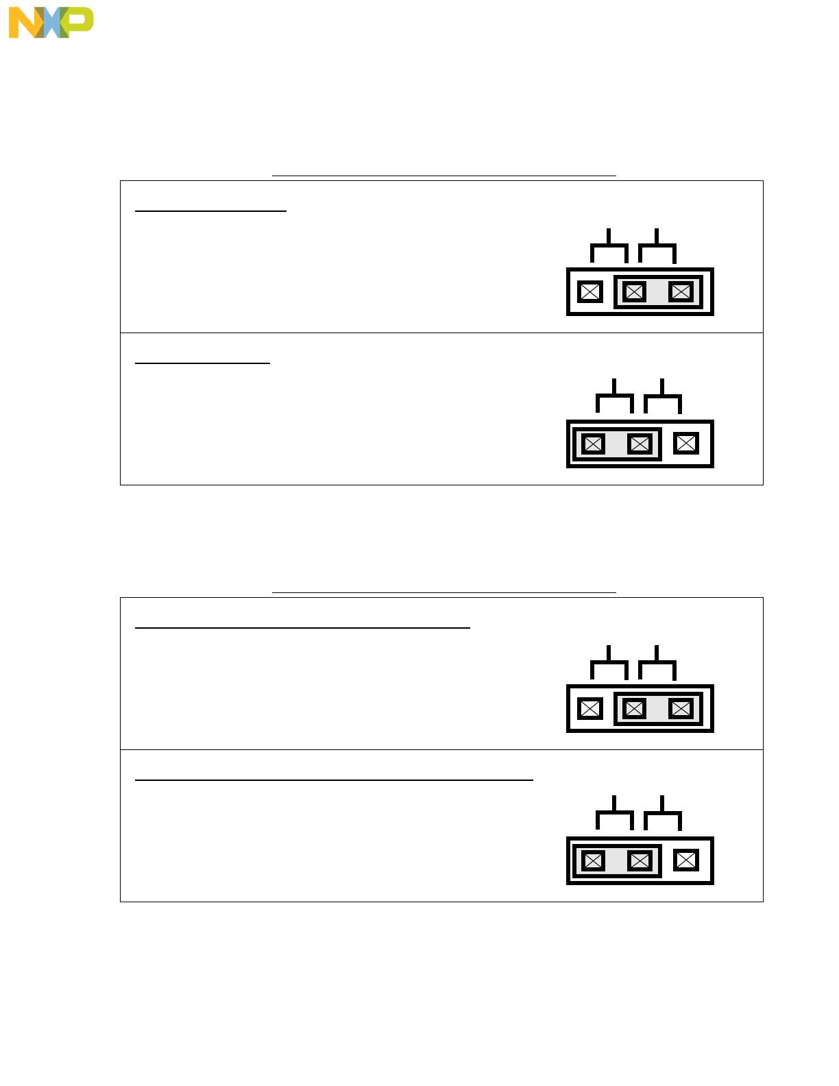
3•2•4 Pchip PLL enable jumper - J2.
The PLL of the Pchip, is controlled by applying or preventing PLL block power, on the VCCSYN pin. The
selection, is done with J2 jumper, as shown in FIGURE 1-10.
FIGURE 1-11 Pchip PLL enable jumper (J2)
3•2•5 PCMCIA power source selection - J3.
The PCMCIA block in the Pchip, can be powered by one of two sources. The first is the board common
VCC supply and the second is an external power, supplied through a PC host, plugged into the PCMCIA
connector. The selection, is done with J3 jumper, as shown in FIGURE 1-12.
FIGURE 1-12 Pchip PLL enable jumper (J3)
1
Pchip PLL - Disabled
Pchip PLL enabled
Pchip PLL
ON OFF
Pchip PLL
ON OFF
When the jumper is installed on pins 2 - 3, the
Pchip PLL is disabled. This actually shorts the
Pchip VCCSYN pin, to ground.
When the jumper is installed between pins 1 - 2,
the Pchip PLL is enabled. This actually connects
VCCSYN pin of the Pchip to VCC.
1
Pchip PCMCIA block is powered by a host PC
Pchip PCMCIA block is powered by board supply board
PCMCIA PWR
INT PC
When the jumper is installed on pins 2 - 3, the
Pchip PCMCIA block, get its power from a host
PC, connected to PCMCIA connector - P4.
When the jumper is installed on pins 1 - 2, the
Pchip PCMCIA block, get its power from the
board common supply.
PCMCIA PWR
INT PC
Frees
cale Semiconductor,
I
Freescale Semiconductor, Inc.
For More Information On This Product,
Go to: www.freescale.com
nc...
OPERATING INSTRUCTIONS
20 M68302FADS User’s Manual
3•2•6 RUN indicator LD1
This yellow indicator is connected to the 302 processor address strobe (AS~) signal. It lit when AS~ is low
(asserted) to indicate a bus activity.
3•2•7 HALT indicator LD2
This red indicator, lit whenever the 302 processor HALT~ pin is low (asserted).
3•2•8 PCOFF indicator LD3
This orange indicator, lit when PCMCIA power control is selected by the DIP-Switch DS1 switch 2
(PCVCCON set to the OFF position) and no external power is detected on the PCMCIA connector - P4.
This is a reminder to the user, that the board is not powered, despite power existence, on P10 connector.
The board would be powered, upon detection of a turned on PC, on the PCMCIA connector - P4.
3•2•9 Power indicator LD4
This green indicator, lit when the board is powered. Please be aware that suppling 5V to P10 connector
does not assure it is powered. When DIP switch DS2 switch number 2, is set to its off position, board power,
is PCMCIA power dependent. The on board relay switches the power off, unless a 5V power is detected
on the PCMCIA port. When DIP switch DS2 switch number 2, is set to its on position, the board is powered
when 5V is supplied trough P10, unconditionally of PCMCIA port status.
Frees
cale Semiconductor,
I
Freescale Semiconductor, Inc.
For More Information On This Product,
Go to: www.freescale.com
nc...
  • Page 1 1
  • Page 2 2
  • Page 3 3
  • Page 4 4
  • Page 5 5
  • Page 6 6
  • Page 7 7
  • Page 8 8
  • Page 9 9
  • Page 10 10
  • Page 11 11
  • Page 12 12
  • Page 13 13
  • Page 14 14
  • Page 15 15
  • Page 16 16
  • Page 17 17
  • Page 18 18
  • Page 19 19
  • Page 20 20
  • Page 21 21
  • Page 22 22
  • Page 23 23
  • Page 24 24
  • Page 25 25
  • Page 26 26
  • Page 27 27
  • Page 28 28
  • Page 29 29
  • Page 30 30
  • Page 31 31
  • Page 32 32
  • Page 33 33
  • Page 34 34
  • Page 35 35
  • Page 36 36
  • Page 37 37
  • Page 38 38
  • Page 39 39
  • Page 40 40
  • Page 41 41
  • Page 42 42
  • Page 43 43
  • Page 44 44
  • Page 45 45
  • Page 46 46
  • Page 47 47
  • Page 48 48
  • Page 49 49
  • Page 50 50
  • Page 51 51
  • Page 52 52
  • Page 53 53
  • Page 54 54
  • Page 55 55
  • Page 56 56
  • Page 57 57
  • Page 58 58
  • Page 59 59
  • Page 60 60
  • Page 61 61
  • Page 62 62
  • Page 63 63
  • Page 64 64
  • Page 65 65
  • Page 66 66
  • Page 67 67
  • Page 68 68
  • Page 69 69
  • Page 70 70
  • Page 71 71
  • Page 72 72
  • Page 73 73
  • Page 74 74
  • Page 75 75
  • Page 76 76
  • Page 77 77
  • Page 78 78
  • Page 79 79
  • Page 80 80
  • Page 81 81
  • Page 82 82
  • Page 83 83
  • Page 84 84
  • Page 85 85
  • Page 86 86
  • Page 87 87
  • Page 88 88
  • Page 89 89
  • Page 90 90
  • Page 91 91
  • Page 92 92
  • Page 93 93
  • Page 94 94
  • Page 95 95
  • Page 96 96
  • Page 97 97
  • Page 98 98
  • Page 99 99

NXP MC68302 Reference guide

Type
Reference guide

Ask a question and I''ll find the answer in the document

Finding information in a document is now easier with AI