
www.dfi .comChapter 1 Introduction
1
HR908-B
COM Express Compact Module
User’s Manual
A25430511

www.dfi .comChapter 1 Introduction
2
Copyright
This publication contains information that is protected by copyright. No part of it may be re-
produced in any form or by any means or used to make any transformation/adaptation without
the prior written permission from the copyright holders.
This publication is provided for informational purposes only. The manufacturer makes no
representations or warranties with respect to the contents or use of this manual and specifi-
cally disclaims any express or implied warranties of merchantability or fitness for any particular
purpose. The user will assume the entire risk of the use or the results of the use of this docu-
ment. Further, the manufacturer reserves the right to revise this publication and make changes
to its contents at any time, without obligation to notify any person or entity of such revisions
or changes.
Changes after the publication’s first release will be based on the product’s revision. The website
will always provide the most updated information.
© 2015. All Rights Reserved.
Trademarks
Product names or trademarks appearing in this manual are for identification purpose only and
are the properties of the respective owners.
COM Express Specification Reference
PICMG
®
COM Express Module
TM
Base Specification.
http://www.picmg.org/
FCC and DOC Statement on Class B
This equipment has been tested and found to comply with the limits for a Class B digital
device, pursuant to Part 15 of the FCC rules. These limits are designed to provide reason-
able protection against harmful interference when the equipment is operated in a residential
installation. This equipment generates, uses and can radiate radio frequency energy and, if not
installed and used in accordance with the instruction manual, may cause harmful interference
to radio communications. However, there is no guarantee that interference will not occur in a
particular installation. If this equipment does cause harmful interference to radio or television
reception, which can be determined by turning the equipment off and on, the user is encour-
aged to try to correct the interference by one or more of the following measures:
• Reorient or relocate the receiving antenna.
• Increase the separation between the equipment and the receiver.
• Connect the equipment into an outlet on a circuit different from that to which the receiver
is connected.
• Consult the dealer or an experienced radio TV technician for help.
Notice:
1. The changes or modifications not expressly approved by the party responsible for compli-
ance could void the user’s authority to operate the equipment.
2. Shielded interface cables must be used in order to comply with the emission limits.

www.dfi .comChapter 1 Introduction
3
Table of Contents
Copyright .............................................................................................................2
Trademarks ........................................................................................................2
FCC and DOC Statement on Class B .....................................................2
About this Manual ..........................................................................................4
Warranty ............................................................................................................4
Static Electricity Precautions ......................................................................4
Safety Measures ..............................................................................................4
About the Package .........................................................................................5
Chapter 1 - Introduction .............................................................................6
Specifications ................................................................................................6
Features ........................................................................................................7
Chapter 2 - Concept ....................................................................... 8
COM Express Module Standards ..............................................................8
Specification Comparison Table ...............................................................9
Chapter 3 - Hardware Installation .............................................. 10
Board Layout ...............................................................................................10
Block Diagram .............................................................................................10
Mechanical Diagram .................................................................................. 11
System Memory ..........................................................................................12
Installing the DIMM Module ........................................................................13
Connectors ...................................................................................................14
CPU Fan Connector .....................................................................................14
COM Express Connectors ............................................................................15
COM Express connector Signal Discription ....................................................16
Standby Power LED ...................................................................................25
Cooling Option ............................................................................................ 25
Installing HR908-B onto a Carrier Board ............................................ 26
Chapter 4 - BIOS Setup ............................................................... 28
Overview ..................................................................................................... 28
AMI BIOS Setup Utility .............................................................................29
Main ..........................................................................................................29
Advanced ................................................................................................... 29
Chipset ......................................................................................................34
Boot...........................................................................................................40
Security ......................................................................................................41
Save & Exit ................................................................................................41
Updating the BIOS ....................................................................................42
Notice: BIOS SPI ROM ............................................................................. 43
Chapter 5 - Supported Software ..........................................................44
Appendix A - nLite and AHCI Installation Guide ........................... 57
nLite ...............................................................................................................57
AHCI ..............................................................................................................61
Appendix B - Watchdog Sample Code ................................................63
Appendix C - System Error Message ...................................................64
Appendix D - Troubleshooting ................................................................ 65

www.dfi .comChapter 1 Introduction
4
About this Manual
An electronic file of this manual is included in the CD. To view the user’s manual in the CD,
insert the CD into a CD-ROM drive. The autorun screen (Main Board Utility CD) will appear.
Click “User’s Manual” on the main menu.
Warranty
1. Warranty does not cover damages or failures that arised from misuse of the product,
inability to use the product, unauthorized replacement or alteration of components and
product specifications.
2. The warranty is void if the product has been subjected to physical abuse, improper instal-
lation, modification, accidents or unauthorized repair of the product.
3. Unless otherwise instructed in this user’s manual, the user may not, under any circum-
stances, attempt to perform service, adjustments or repairs on the product, whether in or
out of warranty. It must be returned to the purchase point, factory or authorized service
agency for all such work.
4. We will not be liable for any indirect, special, incidental or consequencial damages to the
product that has been modified or altered.
Static Electricity Precautions
It is quite easy to inadvertently damage your PC, system board, components or devices even
before installing them in your system unit. Static electrical discharge can damage computer
components without causing any signs of physical damage. You must take extra care in han-
dling them to ensure against electrostatic build-up.
1. To prevent electrostatic build-up, leave the system board in its anti-static bag until you are
ready to install it.
2. Wear an antistatic wrist strap.
3. Do all preparation work on a static-free surface.
4. Hold the device only by its edges. Be careful not to touch any of the components, contacts
or connections.
5. Avoid touching the pins or contacts on all modules and connectors. Hold modules or con-
nectors by their ends.
Safety Measures
To avoid damage to the system:
• Use the correct AC input voltage range.
To reduce the risk of electric shock:
• Unplug the power cord before removing the system chassis cover for installation or servic-
ing. After installation or servicing, cover the system chassis before plugging the power
cord.
Important:
Electrostatic discharge (ESD) can damage your processor, disk drive and other com-
ponents. Perform the upgrade instruction procedures described at an ESD worksta-
tion only. If such a station is not available, you can provide some ESD protection by
wearing an antistatic wrist strap and attaching it to a metal part of the system chas-
sis. If a wrist strap is unavailable, establish and maintain contact with the system
chassis throughout any procedures requiring ESD protection.

www.dfi .comChapter 1 Introduction
5
About the Package
The package contains the following items. If any of these items are missing or damaged,
please contact your dealer or sales representative for assistance.
• One HR908 board
• One QR (Quick Reference)
• One DVD
Optional Items
• COM331-B carrier board kit
• COM101-BAT carrier board kit
• Heat spreader: TBD
• Heat spreader with heat sink and fan: TBD
• Heat sink with fan
The board and accessories in the package may not come similar to the information listed
above. This may differ in accordance with the sales region or models in which it was sold. For
more information about the standard package in your region, please contact your dealer or
sales representative.

www.dfi .comChapter 1 Introduction
6
Audio
• Supports High Defi nition Audio interface
LAN
• Intel
®
82579LM Gigabit Ethernet PHY
• Integrated 10/100/1000 transceiver
• Fully compliant with IEEE 802.3, IEEE 802.3u, IEEE 802.3ab
Serial ATA
• Supports 4 Serial ATA interfaces
• 2 SATA 3.0 with data transfer rate up to 6Gb/s
2 SATA 2.0 with data transfer rate up to 3Gb/s
• Integrated Advanced Host Controller Interface (AHCI) controller
• Supports RAID 0/1/5/10
Watchdog
Timer
• Watchdog timeout programmable via software from 1 to 255 seconds
Expansion
Interfaces
• Supports 8 USB 2.0 interfaces
• Supports 1 PCIe x16 interface
- Supports Gen 3.0 (3rd generation processors)
- Confi gurations (supported only via a riser card):
: One x8 (GFX) and two x4 (I/O)
: Two x8 (GFX, I/O)
: One x16 (GFX, I/O)
• Supports 1 PCIe x4 and 3 PCIe x1 (default); or 7 PCIe x1 interfaces
• Supports LPC interface
• Supports SMBus interface
• Supports I
2
C interface
• Supports 2 serial interfaces (TX/RX)
• Supports 4-bit input and 4-bit output GPIO
Damage Free
Intelligence
• Monitors CPU temperature
• Monitors CPU fan speed
• Monitors Vcore/VGFX/DDR voltages
• Watchdog timer function
OS Support
• Windows XP Professional x86 & SP3 (32-bit)
• Windows XP Professional x64 & SP2 (64-bit)
• Windows 7 Ultimate x86 & SP1 (32-bit)
• Windows 7 Ultimate x64 & SP1 (64-bit)
• Windows 8 Enterprise x86 (32-bit)
• Windows 8 Enterprise x64 (64-bit)
BIOS
• 64Mbit UEFI SPI BIOS
Temperature
• Operating: 0
o
C to 60
o
C
• Storage: -20
o
C to 85
o
C
Humidity
• 10% to 90%
Power
• Input: 12V, 5VSB, VCC_RTC
PCB
• Dimensions
- COM Express
®
Compact
- 95mm (3.74") x 95mm (3.74")
• Compliance
- PICMG COM Express
®
R2.1 Compact form factor, Type 6
Chapter 1 - Introduction
Specifications
Processor
• 3
rd
generation Intel
®
Core
TM
processors (22nm process technology)
: Intel
®
Core
TM
i7-3615QE (6M Cache, up to 3.3GHz); 45W
: Intel
®
Core
TM
i7-3612QE (6M Cache, up to 3.1GHz); 35W
: Intel
®
Core
TM
i7-3555LE (4M Cache, up to 3.2GHz); 25W
: Intel
®
Core
TM
i7-3517UE (4M Cache, up to 2.8GHz); 17W
: Intel
®
Core
TM
i5-3610ME (3M Cache, up to 3.3GHz); 35W
: Intel
®
Core
TM
i3-3120ME (3M Cache, 2.4GHz); 35W
: Intel
®
Core
TM
i3-3217UE (3M Cache, 1.6GHz); 17W
: Intel
®
Celeron
TM
1020E (2M Cache, 2.2GHz); 35W
: Intel
®
Celeron
TM
1047UE (2M Cache, 1.4GHz); 17W
: Intel
®
Celeron
TM
927UE (1M Cache, 1.5GHz); 17W
• 2
nd
generation Intel
®
Core
TM
processors (32nm process technology)
: Intel
®
Core
TM
i7-2715QE (6M Cache, up to 3.0GHz); 45W
: Intel
®
Core
TM
i7-2655LE (4M Cache, up to 2.9GHz); 25W
: Intel
®
Core
TM
i7-2610UE (4M Cache, up to 2.4GHz); 17W
: Intel
®
Core
TM
i5-2515E (3M Cache, up to 3.2GHz); 35W
: Intel
®
Core
TM
i3-2310E (3M Cache, 2.1GHz); 35W
: Intel
®
Core
TM
i3-2340UE (3M Cache, 1.3GHz); 17W
: Intel
®
Celeron
TM
B810E (2M Cache, 1.6GHz); 35W
: Intel
®
Celeron
TM
847E (2M Cache, 1.1GHz); 17W
: Intel
®
Celeron
TM
827E (1.5M Cache, 1.4GHz); 17W
: Intel
®
Celeron
TM
807UE (1M Cache, 1.0GHz); 10W
• BGA 1023 packaging technology
Chipset
• Intel
®
QM67 Express chipset
System Memory
• One 204-pin SODIMM socket
• Supports DDR3 SODIMM
•Supports DDR3L SODIMM
- 1066/1333MHz when operating at 1.35V
- 1066/1333/1600MHz when operating at 1.5V
• Supports up to 8GB system memory
• DRAM device technologies: 1Gb, 2Gb and 4Gb DDR3 DRAM technologies are
supported for x8 and x16 devices, unbuffered, non-ECC
Graphics
• Intel
®
HD Graphics 4000 (3rd generation processors)
• Intel
®
HD Graphics 3000 (2nd generation processors)
• Intel
®
HD Graphics (Intel
®
Celeron
TM
processors)
• Supports LVDS, VGA, and DDI interfaces
• VGA: resolution up to 1920x1200 @ 60Hz
• LVDS: Single Channel - 18/24-bit; Dual Channel - 36/48-bit, resolution up to
1920x1200 @ 60Hz
• Digital Display Interfaces: HDMI, DVI, DP and SDVO
• HDMI, DVI, DP: resolution up to 1920x1200 @ 60Hz
• Intel
®
Clear Video Technology
• DirectX Video Acceleration (DXVA) for accelerating video processing
- Full AVC/VC1/MPEG2 HW Decode
• Supports DirectX 11/10.1/10/9 and OpenGL 3.0 (3rd generation processors)
• Supports DirectX 10.1/10/9 and OpenGL 3.0 (2nd generation processors)
3
rd
Generation Processors 2
nd
Generation Processors
DDR3 1066/1333/1600MHz DDR3 1066/1333MHz (i5/i3/Celeron)
DDR3 1600MHz (i7)
Chapter 1

www.dfi .comChapter 1 Introduction
7
Chapter 1
Note:
Due to the limitation of chipset QM67, 3 display features will not be supported.
Features
• Watchdog Timer
The Watchdog Timer function allows your application to regularly “clear” the system at the set
time interval. If the system hangs or fails to function, it will reset at the set time interval so
that your system will continue to operate.
• DDR3
DDR3 delivers increased system bandwidth and improved performance. The advantages of
DDR3 are its higher bandwidth and its increase in performance at a lower power than DDR2.
• Graphics
The integrated Intel
®
HD graphics engine delivers an excellent blend of graphics performance
and features to meet business needs. It provides excellent video and 3D graphics with out-
standing graphics responsiveness. These enhancements deliver the performance and compat-
ibility needed for today’s and tomorrow’s business applications. It supports LVDS, VGA and DDI
interfaces.
• Serial ATA
Serial ATA is a storage interface that is compliant with SATA 1.0a specification. With speed of
up to 3Gb/s (SATA 2.0) and 6Gb/s (SATA 3.0), it improves hard drive performance faster than
the standard parallel ATA whose data transfer rate is 100MB/s. The bandwidth of the SATA 3.0
will be limited by carrier board design.
• Gigabit LAN
The Intel 82579LM Gigabit LAN controller supports up to 1Gbps data transmission.

www.dfi .comChapter 2 Concept
8
Chapter 2
Chapter 2 - Concept
106.00
91.00
70.00
51.00
4.00
18.00
6.00
0.00
16.50
4.00
0.00
Extended
BasicCompact
Mini
74.20
80.00
91.00
121.00
151.00
Common for all Form Factors
Extended only
Basic only
Compact only
Compact and Basic only
Mini only
COM Express Module Standards
The figure below shows the dimensions of the different types of COM Express modules.
HR908-B is a COM Express Compact module. The dimension is 95mm x 95mm.

www.dfi .comChapter 2 Concept
9
Chapter 2
Specification Comparison Table
Module Pin-out - Required and Optional Features C-D Connector. PICMG
®
COM.0Revision 2.1
The table below shows the COM Express standard specifications and the corresponding specifications supported on the HR908-B module.
• 5 Indicates 12V-tolerant features on former VCC_12V signals.
• 6 Cells in the connected columns spanning rows provide a rough approximation of features
sharing connector pins.
Connector Feature
COM Express Module Base
Specification Type 6
(No IDE or PCI, add DDI+ USB3)
Min
/
Max
DFI HR908-B
Type 6
A-B
A-B PCI Express Lanes 0 - 5 1 / 6 6
A-B LVDS Channel A 0 / 1 1
A-B LVDS Channel B 0 / 1 1
A-B eDP on LVDS CH A pins 0 / 1 0
A-B VGA Port 0 / 1 1
A-B TV-Out NA NA
A-B DDI 0 NA NA
A-B
5
Serial Ports 1 - 2 0 / 2 2
A-B CAN interface on SER1 0 / 1 0
A-B SATA / SAS Ports 1 / 4 4
A-B AC’97 / HDA Digital Interface 0 / 1 1
A-B USB 2.0 Ports 4 / 8 8
A-B USB Client 0 / 1 0
A-B USB 3.0 Ports NA NA
A-B LAN Port 0 1 / 1 1
A-B Express Card Support 1 / 2 2
A-B LPC Bus 1 / 1 1
A-B SPI 1 / 2 1
A-B
SDIO (muxed on GPIO) 0 / 1 0
General Purpose I/O 8 / 8 8
A-B SMBus 1 / 1 1
A-B I2C 1 / 1 1
A-B Watchdog Timer 0 / 1 1
A-B Speaker Out 1 / 1 1
A-B External BIOS ROM Support 0 / 2 0
A-B Reset Functions 1 / 1 1
A-B
6
System I/O
System Management
Connector Feature
COM Express Module Base
Specification Type 6
(No IDE or PCI, add DDI+ USB3)
Min
/
Max
DFI HR908-B
Type 6
A-B
A-B Thermal Protection 0 / 1
1
A-B Battery Low Alarm 0 / 1
1
A-B Suspend/Wake Signals 0 / 3
2
A-B Power Button Support 1 / 1
1
A-B Power Good 1 / 1
1
A-B VCC_5V_SBY Contacts 4 / 4
4
A-B
5
Sleep Input 0 / 1
1
A-B
5
Lid Input 0 / 1
1
A-B
5
Fan Control Signals 0 / 2
2
A-B Trusted Platform Modules 0 / 1
0
A-B
A-B VCC_12V Contacts 12 / 12
12
Power Management
Power
Connector Feature
COM Express Module Base
Specification Type 6
(No IDE or PCI, add DDI+ USB3)
Min
/
Max
DFI HR908-B
Type 6
C-D
PCI Express Lanes 16 - 31 0 / 16
0
PCI Express Graphics (PEG) 0 / 1
1
Muxed SDVO Channels 1 - 2 NA NA
PCI Express Lanes 6 - 15 0 / 2
2
PCI Bus - 32 Bit NA NA
PATA Port NA NA
LAN Ports 1 - 2 NA NA
DDIs 1 - 3 0 / 3
3
USB 3.0 Ports 0 / 4
N
A
C-D
C-D VCC_12V Contacts 12 / 12
12
Power
C-D
6
C-D
6
System I/O

www.dfi .comChapter 3 Hardware Installation
10
Chapter 3
Chapter 3 - Hardware Installation
Board Layout
Top View
Bottom View
Block Diagram
COM Express connector
C1
D1
C110
D110
B1
B110
A1
A110
COM Express connector
IMVP7
(Vcore,Vgfx)
PEG 16x LANES
PCIe x1 6x
CRT
USB 2.0 8x
SATA 2.0 2x, SATA 3.0 2x
LVDS (Dual Channel)
Channel A (DDR3)
1066/1333/1600MHz
Channel A (DDR3L)
1066/1333MHz
z
3
rd
/2
nd
Generation
Intel
®
Core™ i7/i5/i3
CORE
Processor
CORE CORE CORE
Graphics
CORE
Memory
Controller
DMI
(Direct Media
Interface)
Intel
®
FDI
(Flexible Display
Interface)
106
DDR3/
DDR3L
SODIMM
Mobile Intel
®
QM67
(Platform
Controller Hub)
SM Bus
HD Audio
LPC Bus
Intel
®
GLAN
PHY 82579LM
LAN Ports
A / B
C / D
PEG
16x
LANES
HD
Audio
LPC Bus
USB
2
.
0
8x
S
20
2
S
3
02
SATA
2
.
0
2x
,
SATA
3
.
0
2x
LVDS (D l Ch l)
CRT
LVDS
(Dual
Channel)
PCI 1
6
CRT
PCIe
x1
6x
LAN
Ports
PCIe x1, Lane 8
SM
Bus
HD A
di
DDP Port C
PCIe x1 Lane 7
Serial Port 2x
Seri
al P
ort
2x
LPC
Bus
GPIO/
WDT/I
2
C
SPI
Si
lP
t
2
SPI
System Fan PWM/TACH_IN
System
Fan
PWM/TACH
_
IN
DDP
Port
C
DDP Port D
DDP
Port
D
DDP Port B/SDVO Port B
DDP
Port
B/SDVO
Port
B
PCIe
x1
Lane
7
DDR3 SODIMM
iTE
IT8518E
Intel
QM67
1
CPU fan
Intel 82579LM
SPI Flash
BIOS
Standby Power LED
BGA 1023
i3/i5/i7
Intel

www.dfi .comChapter 3 Hardware Installation
11
Chapter 3
Mechanical Diagram
HR908-B Module with Heat Sink
Side View of the Module with Heat Sink and Carrier Board
HR908-B Module
95.00
95.00
Bottom View
Top View
Ø2
.70(*4 pcs)
0.00
12.50
70.20
0.00
0.00
4.00
87.00
91.00
76.00
4.00
0.00
91.00
4.00
87.00
87.00
91.00
91.00
0.00
4.00
0.00
2.00
14.00
4.00
87.00
95.00
23.60
33.60
2.00
35.60
4.00
76.00
83.50
4.00
87.00
95.00
Module PCB
The height of the highest parts
3.50
1.60
5.0 or 8.0 mm
Cooler
Module PCB
CarrierBoard
standoff
33.60

www.dfi .comChapter 3 Hardware Installation
12
Chapter 3
System Memory
Standby
Power LED
The system board is equipped with one 204-pin SODIMM socket that support DDR3 memory
modules.
DDR3
Important:
Electrostatic discharge (ESD) can damage your board, processor, disk drives, add-in
boards, and other components. Perform installation procedures at an ESD workstation
only. If such a station is not available, you can provide some ESD protection by wear-
ing an antistatic wrist strap and attaching it to a metal part of the system chassis. If
a wrist strap is unavailable, establish and maintain contact with the system chassis
throughout any procedures requiring ESD protection.
Important:
When the Standby Power LED lit red, it indicates that there is power on the board.
Power-off the PC then unplug the power cord prior to installing any devices. Failure to
do so will cause severe damage to the board and components.
System Memory

www.d.comChapter 3 Hardware Installation
13
Chapter 3
Installing the DIMM Module
1. Make sure the PC and all other peripheral devices connected to it has been powered down.
2. Disconnect all power cords and cables.
3. Locate the SODIMM socket on the system board.
4. Note the key on the socket. The key ensures the module can be plugged into the socket in
only one direction.
6. Push down the module until the clips at each end of the socket lock into position. You will
hear a distinctive “click”, indicating the module is correctly locked into position.
5. Grasping the module by its edges, align the module into the socket at an approximately 30
degrees angle. Apply firm even pressure to each end of the module until it slips down into
the socket. The contact fingers on the edge of the module will almost completely disappear
inside the socket.
Note:
The system board used in the following illustrations may not resemble the actual one.
These illustrations are for reference only.
Clip
Clip

www.dfi .comChapter 3 Hardware Installation
14
Chapter 3
Connectors
CPU Fan Connector
Connect the CPU fan’s cable connector to the CPU fan connector on the board. The cooling fan
will provide adequate airflow throughout the chassis to prevent overheating the CPU and board
components.
BIOS Setting
“Module Board H/W Monitor” submenu in the Advanced menu of the BIOS will display the cur-
rent speed of the cooling fan. Refer to chapter 3 of the manual for more information
.
3
1
Sense
Power
Ground
COM Express Connectors
The COM Express connectors are used to interface the HR908-B COM Express board to a car-
rier board. Connect the COM Express connectors (lcoated on the solder side of the board) to
the COM Express connectors on the carrier board.
Refer to the “Installing HR908-B onto a Carrier Board” section for more information.
COM Express Connectors
Refer to the following pages for the pin functions of these connectors.

www.dfi .comChapter 3 Hardware Installation
15
Chapter 3
COM Express Connectors
C1 GND (FIXED) D1 GND (FIXED) C56 PEG_RX1- D56 PEG_TX1-
C2 GND D2 GND C57 TYPE1# D57 TYPE2#
C3 NA D3 NA C58 PEG_RX2+ D58 PEG_TX2+
C4 NA D4 NA C59 PEG_RX2- D59 PEG_TX2-
C5 GND D5 GND C60 GND (FIXED) D60 GND (FIXED)
C6 NA D6 NA C61 PEG_RX3+ D61 PEG_TX3+
C7 NA D7 NA C62 PEG_RX3- D62 PEG_TX3-
C8 GND D8 GND C63 RSVD D63 RSVD
C9 NA D9 NA C64 RSVD D64 RSVD
C10 NA D10 NA C65 PEG_RX4+ D65 PEG_TX4+
C11 GND (FIXED) D11 GND (FIXED) C66 PEG_RX4- D66 PEG_TX4-
C12 NA D12 NA C67 NC D67 GND
C13 NA D13 NA C68 PEG_RX5+ D68 PEG_TX5+
C14 GND D14 GND C69 PEG_RX5- D69 PEG_TX5-
C15 DDI1_PAIR6+ D15 DDI1_CTRLCLK_AUX+ C70 GND (FIXED) D70 GND (FIXED)
C16 DDI1_PAIR6- D16 DDI1_CTRLDATA_AUX- C71 PEG_RX6+ D71 PEG_TX6+
C17 RSVD D17 RSVD C72 PEG_RX6- D72 PEG_TX6-
C18 RSVD D18 RSVD C73 GND D73 GND
C19 PCIE_RX6+ D19 PCIE_TX6+ C74 PEG_RX7+ D74 PEG_TX7+
C20 PCIE_RX6- D20 PCIE_TX6- C75 PEG_RX7- D75 PEG_TX7-
C21 GND (FIXED) D21 GND (FIXED) C76 GND D76 GND
C22 PCIE_RX7+ D22 PCIE_TX7+ C77 RSVD D77 IDE_CBLID#
C23 PCIE_RX7- D23 PCIE_TX7- C78 PEG_RX8+ D78 PEG_TX8+
C24 DDI1_HPD D24 RSVD C79 PEG_RX8- D79 PEG_TX8-
C25 DDI1_PAIR4+ D25 RSVD C80 GND (FIXED) D80 GND (FIXED)
C26 DDI1_PAIR4- D26 DDI1_PAIR0+ C81 PEG_RX9+ D81 PEG_TX9+
C27 RSVD D27 DDI1_PAIR0- C82 PEG_RX9- D82 PEG_TX9-
C28 RSVD D28 RSVD C83 TPM_PP D83 RSVD
C29 DDI1_PAIR5+ D29 DDI1_PAIR1+ C84 GND D84 GND
C30 DDI1_PAIR5- D30 DDI1_PAIR1- C85 PEG_RX10+ D85 PEG_TX10+
C31 GND (FIXED) D31 GND (FIXED) C86 PEG_RX10- D86 PEG_TX10-
C32 DDI2_CTRLCLK_AUX+ D32 DDI1_PAIR2+ C87 GND D87 GND
C33 DDI2_CTRLDATA_AUX- D33 DDI1_PAIR2- C88 PEG_RX11+ D88 PEG_TX11+
C34 DDI2_DDC_AUX_SEL D34 DDI1_DDC_AUX_SEL C89 PEG_RX11- D89 PEG_TX11-
C35 RSVD D35 RSVD C90 GND (FIXED) D90 GND (FIXED)
C36 DDI3_CTRLCLK_AUX+ D36 DDI1_PAIR3+ C91 PEG_RX12+ D91 PEG_TX12+
C37 DDI3_CTRLDATA_AUX- D37 DDI1_PAIR3- C92 PEG_RX12- D92 PEG_TX12-
C38 DDI3_DDC_AUX_SEL D38 RSVD C93 GND D93 GND
C39 DDI3_PAIR0+ D39 DDI2_PAIR0+ C94 PEG_RX13+ D94 PEG_TX13+
C40 DDI3_PAIR0- D40 DDI2_PAIR0- C95 PEG_RX13- D95 PEG_TX13-
C41 GND (FIXED) D41 GND (FIXED) C96 GND D96 GND
C42 DDI3_PAIR1+ D42 DDI2_PAIR1+ C97 RSVD D97 RSVD
C43 DDI3_PAIR1- D43 DDI2_PAIR1- C98 PEG_RX14+ D98 PEG_TX14+
C44 DDI3_HPD D44 DDI2_HPD C99 PEG_RX14- D99 PEG_TX14-
C45 RSVD D45 RSVD C100 GND (FIXED) D100 GND (FIXED)
C46 DDI3_PAIR2+ D46 DDI2_PAIR2+ C101 PEG_RX15+ D101 PEG_TX15+
C47 DDI3_PAIR2- D47 DDI2_PAIR2- C102 PEG_RX15- D102 PEG_TX15-
C48 RSVD D48 RSVD C103 GND D103 GND
C49 DDI3_PAIR3+ D49 DDI2_PAIR3+ C104 VCC_12V D104 VCC_12V
C50 DDI3_PAIR3- D50 DDI2_PAIR3- C105 VCC_12V D105 VCC_12V
C51 GND (FIXED) D51 GND (FIXED) C106 VCC_12V D106 VCC_12V
C52 PEG_RX0+/ D52 PEG_TX0+ C107 VCC_12V D107 VCC_12V
C53 PEG_RX0- D53 PEG_TX0- C108 VCC_12V D108 VCC_12V
C54 TYPE0# D54 PEG_LANE_RV# C109 VCC_12V D109 VCC_12V
C55 PEG_RX1+ D55 PEG_TX1+ C110 GND (FIXED) D110 GND (FIXED)
Row C Row DRow C Row D
A1 GND (FIXED) B1 GND (FIXED) A56 PCIE_TX4- B56 PCIE_RX4-
A2 GBE0_MDI3- B2 GBE0_ACT# A57 GND B57 GPO2
A3 GBE0_MDI3+ B3 LPC_FRAME# A58 PCIE_TX3+ B58 PCIE_RX3+
A4 GBE0_LINK100# B4 LPC_AD0 A59 PCIE_TX3- B59 PCIE_RX3-
A5 GBE0_LINK1000# B5 LPC_AD1 A60 GND (FIXED) B60 GND (FIXED)
A6 GBE0_MDI2- B6 LPC_AD2 A61 PCIE_TX2+ B61 PCIE_RX2+
A7 GBE0_MDI2+ B7 LPC_AD3 A62 PCIE_TX2- B62 PCIE_RX2-
A8 GBE0_LINK# B8 LPC_DRQ0# A63 GPI1 B63 GPO3
A9 GBE0_MDI1- B9 LPC_DRQ1# A64 PCIE_TX1+ B64 PCIE_RX1+
A10 GBE0_MDI1+ B10 LPC_CLK A65 PCIE_TX1- B65 PCIE_RX1-
A11 GND (FIXED) B11 GND (FIXED) A66 GND B66 WAKE0#
A12 GBE0_MDI0- B12 PWRBTN# A67 GPI2 B67 WAKE1#
A13 GBE0_MDI0+ B13 SMB_CK A68 PCIE_TX0+ B68 PCIE_RX0+
A14 GBE0_CTREF B14 SMB_DAT A69 PCIE_TX0- B69 PCIE_RX0-
A15 SUS_S3# B15 SMB_ALERT# A70 GND(FIXED) B70 GND (FIXED)
A16 SATA0_TX+ B16 SATA1_TX+ A71 LVDS_A0+ B71 LVDS_B0+
A17 SATA0_TX- B17 SATA1_TX- A72 LVDS_A0- B72 LVDS_B0-
A18 SUS_S4# B18 SUS_STAT# A73 LVDS_A1+ B73 LVDS_B1+
A19 SATA0_RX+ B19 SATA1_RX+ A74 LVDS_A1- B74 LVDS_B1-
A20 SATA0_RX- B20 SATA1_RX- A75 LVDS_A2+ B75 LVDS_B2+
A21 GND (FIXED) B21 GND (FIXED) A76 LVDS_A2- B76 LVDS_B2-
A22 SATA2_TX+ B22 SATA3_TX+ A77 LVDS_VDD_EN B77 LVDS_B3+
A23 SATA2_TX- B23 SATA3_TX- A78 LVDS_A3+ B78 LVDS_B3-
A24 SUS_S5# B24 PWR_OK A79 LVDS_A3- B79 LVDS_BKLT_EN
A25 SATA2_RX+ B25 SATA3_RX+ A80 GND (FIXED) B80 GND (FIXED)
A26 SATA2_RX- B26 SATA3_RX- A81 LVDS_A_CK+ B81 LVDS_B_CK+
A27 BATLOW# B27 WDT A82 LVDS_A_CK- B82 LVDS_B_CK-
A28 (S)ATA_ACT# B28 AC/HDA _SDIN2 A83 LVDS_I2C_CK B83
LVDS BKLT CTRL
A29 AC/HDA_SYNC B29 AC/HDA _SDIN1 A84 LVDS_I2C_DAT B84 VCC_5V_SBY
A30 AC/HDA _RST# B30 AC/HDA _SDIN0 A85 GPI3 B85 VCC_5V_SBY
A31 GND (FIXED) B31 GND (FIXED) A86 RSVD B86 VCC_5V_SBY
A32 AC/HDA _BITCLK B32 SPKR A87 RSVD B87 VCC_5V_SBY
A33 AC/HDA _SDOUT B33 I2C_CK A88 PCIE0_CK_REF+ B88 BIOS_DIS1#
A34 BIOS_DIS0# B34 I2C_DAT A89 PCIE0_CK_REF- B89 VGA_RED
A35 THRMTRIP# B35 THRM# A90 GND (FIXED) B90 GND (FIXED)
A36 USB6- B36 USB7- A91 SPI_POWER B91 VGA_GRN
A37 USB6+ B37 USB7+ A92 SPI_MISO B92 VGA_BLU
A38 USB_6_7_OC# B38 USB_4_5_OC# A93 GPO0 B93 VGA_HSYNC
A39 USB4- B39 USB5- A94 SPI_CLK B94 VGA_VSYNC
A40 USB4+ B40 USB5+ A95 SPI_MOSI B95 VGA_I2C_CK
A41 GND (FIXED) B41 GND (FIXED) A96 TPM_PP B96 VGA_I2C_DAT
A42 USB2- B42 USB3- A97 TYPE10# B97 SPI_CS#
A43 USB2+ B43 USB3+ A98 SER0_TX B98 RSVD
A44 USB_2_3_OC# B44 USB_0_1_OC# A99 SER0_RX B99 RSVD
A45 USB0- B45 USB1- A100 GND (FIXED) B100 GND (FIXED)
A46 USB0+ B46 USB1+ A101 SER1_TX B101 FAN_PWMOUT
A47 VCC_RTC B47 EXCD1_PERST# A102 SER1_RX B102 FAN_TACHIN
A48 EXCD0_PERST# B48 EXCD1_CPPE# A103 LID# B103 SLEEP#
A49 EXCD0_CPPE# B49 SYS_RESET# A104 VCC_12V B104 VCC_12V
A50 LPC_SERIRQ B50 CB_RESET# A105 VCC_12V B105 VCC_12V
A51 GND (FIXED) B51 GND (FIXED) A106 VCC_12V B106 VCC_12V
A52 PCIE_TX5+ B52 PCIE_RX5+ A107 VCC_12V B107 VCC_12V
A53 PCIE_TX5- B53 PCIE_RX5- A108 VCC_12V B108 VCC_12V
A54 GPI0 B54 GPO1 A109 VCC_12V B109 VCC_12V
A55 PCIE_TX4+ B55 PCIE_RX4+ A110 GND (FIXED) B110 GND (FIXED)
Row A Row B Row A Row B

www.d.comChapter 3 Hardware Installation
16
Chapter 3
COM Express Connectors Signal Description
Signal Pin# Module Pin Type Pwr Rail /Tolerance HR908 Carrier Board Description
AC/HAD_RST# A30 O CMOS 3.3V Suspend/3.3V Connect to CODEC pin 11 RESET# Reset output to CODEC, active low.
AC/HDA_SYNC A29 O CMOS 3.3V/3.3V PU 1K to 3.3VSB Connect to CODEC pin 10 SYNC Sample-synchronization signal to the CODEC(s).
AC/HDA_BITCLK A32 I/O CMOS 3.3V/3.3V Connect to CODEC pin 6 BIT_CLK Serial data clock generated by the external CODEC(s).
AC/HDA_SDOUT A33 O CMOS 3.3V/3.3V Connect to CODEC pin 5 SDATA_OUT Serial TDM data output to the CODEC.
AC/HDA_SDIN2 B28 I/O CMOS 3.3V Suspend/3.3V Connect 33 Ω in series to CODEC2 pin 8 SDATA_IN
AC/HDA_SDIN1 B29 I/O CMOS 3.3V Suspend/3.3V Connect 33 Ω in series to CODEC1 pin 8 SDATA_IN
AC/HDA_SDIN0 B30 I/O CMOS 3.3V Suspend/3.3V Connect 33 Ω in series to CODEC0 pin 8 SDATA_IN
Signal Pin# Module Pin Type Pwr Rail /Tolerance HR908 Carrier Board Description
GBE0_MDI0+ A13 I/O Analog 3.3V max Suspend
GBE0_MDI0- A12 I/O Analog 3.3V max Suspend
GBE0_MDI1+ A10 I/O Analog 3.3V max Suspend
GBE0_MDI1- A9 I/O Analog 3.3V max Suspend
GBE0_MDI2+ A7 I/O Analog 3.3V max Suspend
GBE0_MDI2- A6 I/O Analog 3.3V max Suspend
GBE0_MDI3+ A3 I/O Analog 3.3V max Suspend
GBE0
_
MDI3-
A
2I
/
O Analo
g
3.3V max Sus
p
end
GBE0_ACT# B2 OD CMOS 3.3V Suspend/3.3V Connect to LED and recommend current limit resistor 150Ω to 3.3VSB Gigabit Ethernet Controller 0 activity indicator, active low.
GBE0_LINK# A8 OD CMOS 3.3V Suspend/3.3V NC Gigabit Ethernet Controller 0 link indicator, active low.
GBE0_LINK100# A4 OD CMOS 3.3V Suspend/3.3V Connect to LED and recommend current limit resistor 150Ω to 3.3VSB Gigabit Ethernet Controller 0 1000 Mbit / sec link indicator, active low.
GBE0_LINK1000# A5 OD CMOS 3.3V Suspend/3.3V Connect to LED and recommend current limit resistor 150Ω to 3.3VSB Gigabit Ethernet Controller 0 1000 Mbit / sec link indicator, active low.
Signal Pin# Module Pin Type Pwr Rail /Tolerance HR908 Carrier Board Description
SATA0_TX+ A16 O SATA AC coupled on Module AC Coupling capacitor
SATA0_TX- A17 O SATA AC coupled on Module AC Coupling capacitor
SATA0_RX+ A19 I SATA AC coupled on Module AC Coupling capacitor
SATA0_RX- A20 I SATA AC coupled on Module AC Coupling capacitor
SATA1_TX+ B16 O SATA AC coupled on Module AC Coupling capacitor
SATA1_TX- B17 O SATA AC coupled on Module AC Coupling capacitor
SATA1_RX+ B19 I SATA AC coupled on Module AC Coupling capacitor
SATA1_RX- B20 I SATA AC coupled on Module AC Coupling capacitor
SATA2_TX+ A22 O SATA AC coupled on Module AC Coupling capacitor
SATA2_TX- A23 O SATA AC coupled on Module AC Coupling capacitor
SATA2_RX+ A25 I SATA AC coupled on Module AC Coupling capacitor
SATA2_RX- A26 I SATA AC coupled on Module AC Coupling capacitor
SATA3_TX+ B22 O SATA AC coupled on Module AC Coupling capacitor
SATA3_TX- B23 O SATA AC coupled on Module AC Coupling capacitor
SATA3_RX+ B25 I SATA AC coupled on Module AC Coupling capacitor
SATA3_RX- B26 I SATA AC coupled on Module AC Coupling capacitor
ATA_ACT# A28 I/O CMOS 3.3V / 3.3V PU 10K to 3.3V Connect to LED and recommend current limit resistor 220Ω to 3.3V ATA (parallel and serial) or SAS activity indicator, active low.
Signal Pin# Module Pin Type Pwr Rail /Tolerance HR908 Carrier Board Description
PCIE_TX0+ A68 AC Coupling capacitor
PCIE_TX0- A69 AC Coupling capacitor
PCIE_RX0+ B68
PCIE_RX0- B69
PCIE_TX1+ A64 AC Coupling capacitor
PCIE_TX1- A65 AC Coupling capacitor
PCIE_RX1+ B64
PCIE_RX1- B65
PCIE_TX2+ A61 AC Coupling capacitor
PCIE_TX2- A62 AC Coupling capacitor
PCIE_RX2+ B61
PCIE_RX2- B62
PCIE_TX3+ A58 AC Coupling capacitor
PCIE_TX3- A59 AC Coupling capacitor
PCIE_RX3+ B58
PCIE_RX3- B59
PCIE_TX4+ A55 AC Coupling capacitor
PCIE_TX4- A56 AC Coupling capacitor
PCIE_RX4+ B55
PCIE_RX4- B56
PCIE_TX5+ A52 AC Coupling capacitor
PCIE_TX5- A53 AC Coupling capacitor
PCIE_RX5+ B52
PCIE_RX5- B53
PCIE_TX6+ D19 AC Coupling capacitor
PCIE_TX6- D20 AC Coupling capacitor
PCIE_RX6+ C19
PCIE_RX6- C20
PCIE_TX7+ D22 NA
PCIE_TX7- D23 NA
PCIE_RX7+ C22 NA
PCIE_RX7- C23 NA
PCIE0_CK_REF+ A88
PCIE0_CK_REF- A89
Signal Pin# Module Pin Type Pwr Rail /Tolerance HR908 Carrier Board Description
PEG_TX0+ D52 AC Coupling capacitor
PEG_TX0- D53 AC Coupling capacitor
PEG_RX0+ C52
PEG_RX0- C53
PEG_TX1+ D55 AC Coupling capacitor
PEG_TX1- D56 AC Coupling capacitor
PEG_RX1+ C55
PEG_RX1- C56
PEG_TX2+ D58 AC Coupling capacitor
PEG_TX2- D59 AC Coupling capacitor
PEG_RX2+ C58
PEG_RX2- C59
PEG_TX3+ D61 AC Coupling capacitor
PEG_TX3- D62 AC Coupling capacitor
PEG_RX3+ C61
PEG_RX3- C62
PEG_TX4+ D65 AC Coupling capacitor
PEG_TX4- D66 AC Coupling capacitor
PEG_RX4+ C65
PEG_RX4- C66
PEG_TX5+ D68 AC Coupling capacitor
PEG_TX5- D69 AC Coupling capacitor
PEG_RX5+ C68
PEG_RX5- C69
PEG_TX6+ D71 AC Coupling capacitor
PEG_TX6- D72 AC Coupling capacitor
PEG_RX6+ C71
PEG_RX6- C72
PEG_TX7+ D74 AC Coupling capacitor
PEG_TX7- D75 AC Coupling capacitor
PEG_RX7+ C74
PEG_RX7- C75
PEG_TX8+ D78 AC Coupling capacitor
PEG_TX8- D79 AC Coupling capacitor
PEG_RX8+ C78
PEG_RX8- C79
PEG_TX9+ D81 AC Coupling capacitor
PEG_TX9- D82 AC Coupling capacitor
PEG_RX9+ C81
PEG_RX9- C82
PEG_TX10+ D85 AC Coupling capacitor
PEG_TX10- D86 AC Coupling capacitor
PEG_RX10+ C85
PEG_RX10- C86
PEG_TX11+ D88 AC Coupling capacitor
PEG_TX11- D89 AC Coupling capacitor
PEG_RX11+ C88
PEG_RX11- C89
PEG_TX12+ D91 AC Coupling capacitor
PEG_TX12- D92 AC Coupling capacitor
PEG_RX12+ C91
PEG_RX12- C92
PEG_TX13+ D94 AC Coupling capacitor
PEG_TX13- D95 AC Coupling capacitor
PEG_RX13+ C94
PEG_RX13- C95
PEG_TX14+ D98 AC Coupling capacitor
PEG_TX14- D99 AC Coupling capacitor
PEG_RX14+ C98
PEG_RX14- C99
PEG_TX15+ D101 AC Coupling capacitor
PEG_TX15- D102 AC Coupling capacitor
PEG_RX15+ C101
PEG_RX15- C102
PEG_LANE_RV# D54 I CMOS 3.3V / 3.3V
PCI Express Graphics lane reversal input strap. Pull low on the Carrier
board to reverse lane order.
Signal Pin# Module Pin Type Pwr Rail /Tolerance HR908 Carrier Board Description
EXCD0_CPPE# A49 PU 10k to 3.3V
EXCD1_CPPE# B48 PU 10k to 3.3V
EXCD0_PERST# A48
EXCD1_PERST# B47
Signal Pin# Module Pin Type Pwr Rail /Tolerance HR908 Carrier Board Description
DDI1_PAIR0+/SDVO1_RED+ D26 Connect AC Coupling Capacitors 0.1uF to Device
DDI1
_
PAIR0-
/
SDVO1
_
RED- D27 Connect AC Cou
p
lin
g
Ca
p
acitors 0.1uF to Devic
e
DDI1_PAIR1+/SDVO1_GRN+ D29 Connect AC Coupling Capacitors 0.1uF to Device
DDI1_PAIR1-/SDVO1_GRN- D30 Connect AC Coupling Capacitors 0.1uF to Device
DDI1_PAIR2+/SDVO1_BLU+ D32 Connect AC Coupling Capacitors 0.1uF to Device
DDI1_PAIR2-/SDVO1_BLU- D33 Connect AC Coupling Capacitors 0.1uF to Device
DDI1_PAIR3+/SDVO1_CK+ D36 Connect AC Coupling Capacitors 0.1uF to Device
DDI1_PAIR3-/SDVO1_CK- D37 Connect AC Coupling Capacitors 0.1uF to Device
DDI1_PAIR4+/SDVO1_INT+ C25 Connect AC Coupling Capacitors 0.1uF to Device
DDI1_PAIR4-/SDVO1_INT- C26 Connect AC Coupling Capacitors 0.1uF to Device
DDI1_PAIR5+/SDVO1_TVCLKIN+ C29 Connect AC Coupling Capacitors 0.1uF to Device
DDI1_PAIR5-/SDVO1_TVCLKIN- C30 Connect AC Coupling Capacitors 0.1uF to Device
DDI1_PAIR6+/SDVO1_FLDSTALL+ C15 Connect AC Coupling Capacitors 0.1uF to Device
DDI1_PAIR6-/SDVO1_FLDSTALL- C16 Connect AC Coupling Capacitors 0.1uF to Device
I/O PCIE AC coupled on Module
PD 49.9K to GND
(
S
/
W IC between
Connect to DP AUX+ DP AUX+ function if DDI1_DDC_AUX_SEL is no connect
I/O OD CMOS 3.3V / 3.3V
PU 2.2K to 3.3V, PD 49.9K to
GND
Connect to HDMI/DVI I2C CTRLCLK HDMI/DVI I2C CTRLCLK if DDI1_DDC_AUX_SEL is pulled high
I/O PCIE AC coupled on Module
PU 100K to 3.3V
(S/W IC between
Connect to DP AUX- DP AUX- function if DDI1_DDC_AUX_SEL is no connect
I/O OD CMOS 3.3V / 3.3V
PU 2.2K to 3.3V/PU 100K to
3.3V
(S/W IC between
Connect to HDMI/DVI I2C CTRLDATA HDMI/DVI I2C CTRLDATA if DDI1_DDC_AUX_SEL is pulled high
DDI1_HPD C24 I CMOS 3.3V / 3.3V PD 1M and Connect to device Hot Plug Detect DDI Hot-Plug Detect
DDI1_DDC_AUX_SEL D34 I CMOS 3.3V / 3.3V PD 1M
PU 100K to 3.3V for DDC(HDMI/DVI)
Selects the function of DDI1_CTRLCLK_AUX+ and DDI1_CTRLDATA_AUX-.
DDI[n]_DDC_AUX_SEL shall be pulled to 3.3V on the Carrier with a 100K Ohm
resistor to configure the DDI[n]_AUX pair as the DDC channel.
Carrier DDI
[
n
]
DDC AUX SEL should be connected to
p
in 13 of the Dis
p
la
y
Por
t
DDI2_PAIR0+ D39 Connect AC Coupling Capacitors 0.1uF to Device
DDI2_PAIR0- D40 Connect AC Coupling Capacitors 0.1uF to Device
DDI2_PAIR1+ D42 Connect AC Coupling Capacitors 0.1uF to Device
DDI2_PAIR1- D43 Connect AC Coupling Capacitors 0.1uF to Device
DDI2_PAIR2+ D46 Connect AC Coupling Capacitors 0.1uF to Device
DDI2_PAIR2- D47 Connect AC Coupling Capacitors 0.1uF to Device
DDI2_PAIR3+ D49 Connect AC Coupling Capacitors 0.1uF to Device
DDI2_PAIR3- D50 Connect AC Coupling Capacitors 0.1uF to Device
I/O PCIE AC coupled on Module
PD 49.9K to GND
(S/W IC between
Connect to DP AUX+ DP AUX+ function if DDI2_DDC_AUX_SEL is no connect
I/O OD CMOS 3.3V / 3.3V
PU 2.2K to 3.3V, PD 49.9K to
GND
Connect to HDMI/DVI I2C CTRLCLK HDMI/DVI I2C CTRLCLK if DDI2_DDC_AUX_SEL is pulled high
I/O PCIE AC coupled on Module
PU 100K to 3.3V
(
S
/
W IC between
Connect to DP AUX- DP AUX- function if DDI2_DDC_AUX_SEL is no connect
I/O OD CMOS 3.3V / 3.3V
PU 2.2K to 3.3V/PU 100K to
3.3V
(S/W IC between
Connect to HDMI/DVI I2C CTRLDATA HDMI/DVI I2C CTRLDATA if DDI2_DDC_AUX_SEL is pulled high
DDI3_HPD D44 I CMOS 3.3V / 3.3V PD 1M and Connect to device Hot Plug Detect DDI Hot-Plug Detect
DDI3_DDC_AUX_SEL C34 I CMOS 3.3V / 3.3V PD 1M to GND
PU 100K to 3.3V for DDC(HDMI/DVI)
Selects the function of DDI2_CTRLCLK_AUX+ and DDI2_CTRLDATA_AUX-.
DDI[n]_DDC_AUX_SEL shall be pulled to 3.3V on the Carrier with a 100K Ohm
resistor to configure the DDI[n]_AUX pair as the DDC channel.
Carrier DDI
[
n
]_
DDC
_
AUX
_
SEL should be connected to
p
in 13 of the Dis
p
la
y
Por
t
DDI3_PAIR0+ C39 Connect AC Coupling Capacitors 0.1uF to Device
DDI3_PAIR0- C40 Connect AC Coupling Capacitors 0.1uF to Device
DDI3_PAIR1+ C42 Connect AC Coupling Capacitors 0.1uF to Device
DDI3_PAIR1- C43 Connect AC Coupling Capacitors 0.1uF to Device
DDI3_PAIR2+ C4 Connect AC Coupling Capacitors 0.1uF to Device
DDI3_PAIR2- C47 Connect AC Coupling Capacitors 0.1uF to Device
DDI3_PAIR3+ C49 Connect AC Coupling Capacitors 0.1uF to Device
DDI3_PAIR3- C50 Connect AC Coupling Capacitors 0.1uF to Device
I/O PCIE AC coupled on Module
PD 49.9K to GND
(S/W IC between
Connect to DP AUX+ DP AUX+ function if DDI3_DDC_AUX_SEL is no connect
I/O OD CMOS 3.3V / 3.3V
PU 2.2K to 3.3V, PD 49.9K to
GND
(S/W IC between Rpu/Rpd
Connect to HDMI/DVI I2C CTRLCLK HDMI/DVI I2C CTRLCLK if DDI3_DDC_AUX_SEL is pulled high
I/O PCIE AC coupled on Module
PU 100K to 3.3V
(S/W IC between
Connect to DP AUX- DP AUX- function if DDI3_DDC_AUX_SEL is no connect
I/O OD CMOS 3.3V / 3.3V
PU 2.2K to 3.3V/PU 100K to
3.3V
Connect to HDMI/DVI I2C CTRLDATA HDMI/DVI I2C CTRLDATA if DDI3_DDC_AUX_SEL is pulled high
DDI3_HPD C44 I CMOS 3.3V / 3.3V PD 1M and Connect to device Hot Plug Detect DDI Hot-Plug Detect
DDI3_DDC_AUX_SEL C38 I CMOS 3.3V / 3.3V PD 1M to GND
PU 100K to 3.3V for DDC(HDMI/DVI)
Selects the function of DDI3_CTRLCLK_AUX+ and DDI3_CTRLDATA_AUX-.
DDI[n]_DDC_AUX_SEL shall be pulled to 3.3V on the Carrier with a 100K Ohm
resistor to configure the DDI[n]_AUX pair as the DDC channel.
Carrier DDI
[
n
]
DDC AUX SEL should be connected to
p
in 13 of the Dis
p
la
y
Por
t
Signal Pin# Module Pin Type Pwr Rail /Tolerance HR908 Carrier Board Description
USB0+ A46
USB0- A45
USB1+ B46
USB1- B45
USB2+ A43
USB2- A42
USB3+ B43
USB3- B42
USB4+ A40
USB4- A39
USB5+ B40
USB5- B39
USB6+ A37
USB6- A36
USB7+ B37
USB7- B36
USB_0_1_OC# B44 I CMOS 3.3V Suspend/3.3V PU 10k to 3.3VSB Connect to Overcurrent of USB Power Switch
USB over-current sense, USB channels 0 and 1. A pull-up for this line
shall be present on the Module. An open drain driver from a USB
current monitor on the Carrier Board may drive this line low. Do not
p
ull this line hi
g
h on the Carrier Board.
USB_2_3_OC# A44 I CMOS 3.3V Suspend/3.3V PU 10k to 3.3VSB Connect to Overcurrent of USB Power Switch
USB over-current sense, USB channels 2 and 3. A pull-up for this line
shall be present on the Module. An open drain driver from a USB
current monitor on the Carrier Board may drive this line low. Do not
p
ull this line hi
g
h on the Carrier Board.
USB_4_5_OC# B38 I CMOS 3.3V Suspend/3.3V PU 10k to 3.3VSB Connect to Overcurrent of USB Power Switch
USB over-current sense, USB channels 4 and 5. A pull-up for this line
shall be present on the Module. An open drain driver from a USB
current monitor on the Carrier Board may drive this line low. Do not
p
ull this line hi
g
h on the Carrier Board.
USB_6_7_OC# A38 I CMOS 3.3V Suspend/3.3V PU 10k to 3.3VSB Connect to Overcurrent of USB Power Switch
USB over-current sense, USB channels 6 and 7. A pull-up for this line
shall be present on the Module. An open drain driver from a USB
current monitor on the Carrier Board may drive this line low. Do not
p
ull this line hi
g
h on the Carrier Board.
Signal Pin# Module Pin Type Pwr Rail /Tolerance HR908 Carrier Board Description
LVDS_A0+ A71
LVDS_A0- A72
LVDS_A1+ A73
LVDS_A1- A74
LVDS_A2+ A75
LVDS_A2- A76
LVDS_A3+ A78
LVDS_A3- A79
LVDS_A_CK+ A81
LVDS_A_CK- A82
LVDS_B0+ B71
LVDS_B0- B72
LVDS_B1+ B73
LVDS_B1- B74
LVDS_B2+ B75
LVDS_B2- B76
LVDS_B3+ B77
LVDS_B3- B78
LVDS_B_CK+ B81
LVDS_B_CK- B82
LVDS_VDD_EN A77 O CMOS 3.3V / 3.3V PD 100K to GND Connect to enable control of LVDS panel power circuit LVDS panel power enable
LVDS_BKLT_EN B79 O CMOS 3.3V / 3.3V PD 100K to GND Connect to enable control of LVDS panel backlight power circuit. LVDS panel backlight enable
LVDS_BKLT_CTRL B83 O CMOS 3.3V / 3.3V PD 100K to GND Connect to brightness control of LVDS panel backlight power circuit. LVDS panel backlight brightness control
LVDS_I2C_CK A83 I/O OD CMOS 3.3V / 3.3V PU 2.2K to 3.3V Connect to DDC clock of LVDS panel I2C clock output for LVDS display use
LVDS_I2C_DAT A84 I/O OD CMOS 3.3V / 3.3V PU 2.2K to 3.3V Connect to DDC data of LVDS panel I2C data line for LVDS display use
Signal Pin# Module Pin Type Pwr Rail /Tolerance HR908 Carrier Board Description
LPC_AD0 B4
LPC_AD1 B5
LPC_AD2 B6
LPC_AD3 B7
LPC_FRAME# B3 O CMOS 3.3V / 3.3V LPC frame indicates the start of an LPC cycle
LPC_DRQ0# B8
LPC_DRQ1# B9
LPC_SERIRQ A50 I/O CMOS 3.3V / 3.3V PU 10K to 3.3V LPC serial interrupt
LPC_CLK B10 O CMOS 3.3V / 3.3V LPC clock output - 33MHz nominal
Signal Pin# Module Pin Type Pwr Rail /Tolerance HR908 Carrier Board Description
SPI_CS# B97 O CMOS 3.3V Suspend/3.3V
Connect a series resistor 33Ω
to Carrier Board SPI Device CS# pin
Chip select for Carrier Board SPI - may be sourced from chipset SPI0 or SPI1
SPI_MISO A92 I CMOS 3.3V Suspend/3.3V Connect a series resistor 33Ω
to Carrier Board SPI Device SO pin Data in to Module from Carrier SPI
SPI_MOSI A95 O CMOS 3.3V Suspend/3.3V Connect a series resistor 33Ω
to Carrier Board SPI Device SI pin Data out from Module to Carrier SPI
SPI_CLK A94 O CMOS 3.3V Suspend/3.3V Connect a series resistor 33Ω
to Carrier Board SPI Device SCK pin Clock from Module to Carrier SPI
SPI_POWER A91 O 3.3V Suspend/3.3V
Power supply for Carrier Board SPI – sourced from Module – nominally
3.3V. The Module shall provide a minimum of 100mA on SPI_POWER.
Carriers shall use less than 100mA of SPI_POWER. SPI_POWER
shall only be used to power SPI devices on the Carrier
BIOS_DIS0# A34
BIOS_DIS1# B88
Signal Pin# Module Pin Type Pwr Rail /Tolerance HR908 Carrier Board Description
VGA_RED B89 O Analog Analog PD 150R PD 150R,connect to VGA connector with EMI filter & ESD protect component. Red for monitor. Analog output
VGA_GRN B91 O Analog Analog PD 150R PD 150R,connect to VGA connector with EMI filter & ESD protect component. Green for monitor. Analog output
VGA_BLU B92 O Analog Analog PD 150R PD 150R,connect to VGA connector with EMI filter & ESD protect component. Blue for monitor. Analog output
VGA_HSYNC B93 O CMOS 3.3V / 3.3V Connect to VGA connector with a3.3V Buffer IC to isolate PCH & Display Device Horizontal sync output to VGA monitor
VGA_VSYNC B94 O CMOS 3.3V / 3.3V Connect to VGA connector with a 33V Buffer IC to isolate PCH & Display Device Vertical sync output to VGA monitor
VGA_I2C_CK B95 I/O OD CMOS 3.3V / 3.3V PD 2.2K to 3.3V Connect to VGA connector with a 3.3V to 5V Level shift circuit. DDC clock line (I2C port dedicated to identify VGA monitor capabilities)
VGA_I2C_DAT B96 I/O OD CMOS 3.3V / 3.3V PD 2.2K to 3.3V Connect to VGA connector with a 3.3V to 5V Level shift circuit. DDC data line.
Signal Pin# Module Pin Type Pwr Rail /Tolerance HR908 Carrier Board Description
SER0_TX A98 O CMOS 3.3V/5V PD 4.7K
General purpose serial port 0 transmitter
(
Recommend add Protectin
g
Lo
g
ic Level Si
g
nals on Pins Reclaimed from VCC
_
12V
)
SER0_RX A99 I CMOS 3.3V/5V PU 47K to 3.3V
General purpose serial port 0 receiver
(
Recommend add Protectin
g
Lo
g
ic Level Si
g
nals on Pins Reclaimed from VCC
_
12V
)
SER1_TX A101 O CMOS 3.3V/5V PD 4.7K
General purpose serial port 1 transmitter
(
Recommend add Protectin
g
Lo
g
ic Level Si
g
nals on Pins Reclaimed from VCC
_
12V
)
SER1_RX A102 I CMOS 3.3V/5V PU 47K to 3.3V
General purpose serial port 1 receiver
(
Recommend add Protectin
g
Lo
g
ic Level Si
g
nals on Pins Reclaimed from VCC
_
12V
)
Signal Pin# Module Pin Type Pwr Rail /Tolerance HR908 Carrier Board Description
I2C_CK B33 I/O OD CMOS 3.3V Suspend/3.3V PU 2.2K to 3.3VSB General purpose I2C port clock output
I2C_DAT B34 I/O OD CMOS 3.3V Suspend/3.3V PU 2.2K to 3.3VSB General purpose I2C port data I/O line
SPKR B32 O CMOS 3.3V / 3.3V
Output for audio enunciator - the "speaker" in PC-AT systems.
This port provides the PC beep signal and is mostly intended for
debugging purposes.
WDT B27 O CMOS 3.3V / 3.3V Output indicating that a watchdog time-out event has occurred.
FAN_PWNOUT B101 O OD CMOS 3.3V / 3.3V
Fan speed control. Uses the Pulse Width Modulation (PWM) technique to control the fan's RPM.
(
Recommend add Protectin
g
Lo
g
ic Level Si
g
nals on Pins Reclaimed from VCC
_
12V
)
FAN_TACHIN B102 I OD CMOS 3.3V / 3.3V
Fan tachometer input for a fan with a two pulse output.
(Recommend add Protecting Logic Level Signals on Pins Reclaimed from VCC_12V)
TPM_PP A96 I CMOS 3.3V / 3.3V PD 1M
Trusted Platform Module (TPM) Physical Presence pin. Active high.
TPM chip has an internal pull down. This signal is used to indicate
Physical Presence to the TPM.
Signal Pin# Module Pin Type Pwr Rail /Tolerance HR908 Carrier Board Description
PWRBTN# B12 I CMOS 3.3V Suspend/3.3V PU 10K to 3.3VSB
A falling edge creates a power button event. Power button events can
be used to bring a system out of S5 soft off and other suspend states,
as well as powering the system down.
SYS_RESET# B49 I CMOS 3.3V Suspend/3.3V PU 10K to 3.3V
Reset button input. Active low request for Module to reset and reboot.
May be falling edge sensitive. For situations when SYS_RESET# is
not able to reestablish control of the system, PWR_OK or a power
cycle may be used.
CB_RESET# B50 O CMOS 3.3V Suspend/3.3V PU 10K to 3.3VSB
Reset output from Module to Carrier Board. Active low. Issued by
Module chipset and may result from a low SYS_RESET# input, a low
PWR_OK input, a VCC_12V power input that falls below the minimum
specification, a watchdog timeout, or may be initiated by the Module
software.
PWR_OK B24 I CMOS 3.3V / 3.3V
Power OK from main power supply. A high value indicates that the
power is good. This signal can be used to hold off Module startup to
allow Carrier based FPGAs or other configurable devices time to be
programmed.
SUS_STAT# B18 O CMOS 3.3V Suspend/3.3V Indicates imminent suspend operation; used to notify LPC devices.
SUS_S3# A15 O CMOS 3.3V Suspend/3.3V
Indicates system is in Suspend to RAM state. Active low output. An
inverted copy of SUS_S3# on the Carrier Board may be used to
enable the non-standby power on a typical ATX supply.
SUS_S4# A18 O CMOS 3.3V Suspend/3.3V Indicates system is in Suspend to Disk state. Active low output.
SUS_S5# A24 O CMOS 3.3V Suspend/3.3V Indicates system is in Soft Off state.
WAKE0# B66 I CMOS 3.3V Suspend/3.3V PU 10K to 3.3VSB PCI Express wake up signal.
WAKE1# B67 I CMOS 3.3V Suspend/3.3V PU 10K to 3.3VSB
General purpose wake up signal. May be used to implement wake-up
on PS2 keyboard or mouse activity.
BATLOW# A27 I CMOS 3.3V Suspend/ 3.3V PU 10K to 3.3VSB
Indicates that external battery is low.
This port provides a battery-low signal to the Module for orderly
transitioning to power saving or power cut-off ACPI modes.
LID# A103 I OD CMOS 3.3V Suspend/12V PU 10K to 3.3VSB
LID switch. Low active signal used by the ACPI operating system for a LID switch.
(
Recommend add Protectin
g
Lo
g
ic Level Si
g
nals on Pins Reclaimed from VCC
_
12V
)
SLEEP# B103 I OD CMOS 3.3V Suspend/12V PU 10K to 3.3VSB
Sleep button. Low active signal used by the ACPI operating system to bring the
system to sleep state or to wake it up again.
(Recommend add Protecting Logic Level Signals on Pins Reclaimed from VCC_12V)
THRM# B35 I CMOS 3.3V / 3.3V PU 10K to 3.3V Input from off-Module temp sensor indicating an over-temp situation.
THRMTRIP# A35 O CMOS 3.3V / 3.3V PU 10K to 3.3V Active low output indicating that the CPU has entered thermal shutdown.
SMB_CK B13 I/O OD CMOS 3.3V Suspend/3.3V PU 2.2K to 3.3VSB System Management Bus bidirectional clock line.
SMB_DAT B14 I/O OD CMOS 3.3V Suspend/3.3V PU 2.2K to 3.3VSB System Management Bus bidirectional data line.
SMB_ALERT# B15 I CMOS 3.3V Suspend/3.3V PU 10K to 3.3VSB
System Management Bus Alert – active low input can be used to
generate an SMI# (System Management Interrupt) or to wake the system.
Signal Pin# Module Pin Type Pwr Rail /Tolerance HR908 Carrier Board Description
GPO0 A93
GPO1 B54
GPO2 B57
GPO3 B63
GPI0 A54
GPI1 A63
GPI2 A67
GPI3 A85
Signal Pin# Module Pin Type Pwr Rail /Tolerance HR908 Carrier Board Description
VCC_12V
A
104~A109
B104~B109
C104~C109
D104
~
D109
Power Primary power input: +12V nominal. All available VCC_12V pins on the connector(s) shall be used.
VCC_5V_SBY B84~B87 Power
Standby power input: +5.0V nominal. If VCC5_SBY is used, all
available VCC_5V_SBY pins on the connector(s) shall be used. Only
used for standby and suspend functions. May be left unconnected if
these functions are not used in the system design.
VCC_RTC A47 Power Real-time clock circuit-power input. Nominally +3.0V.
GND
A1, A11, A21, A31,
A41, A51, A57, A60,
A66, A70, A80, A90,
A100, A110, B1,
B11, B21 ,B31, B41,
B51, B60, B70, B80,
B90, B100, B110,
C1, C2, C5, C8, C11,
C14, C21, C31, C41,
C51, C60, C70, C73,
C76, C80, C84, C87,
C90, C93, C96,
C100, C103, C110,
D1, D2, D5, D8,
D11, D14, D21,
D31, D51, D60,
D67, D70, D73,
D76, D80, D84,
D87, D90, D93,
D96, D100, D103,
D110
Power
Ground - DC power and signal and AC signal return path.
All available GND connector pins shall be used and tied to Carrier
Board GND plane.
Connect to PCIE device or slot
Device - Connect AC Coupling cap 0.1uF
Slot - Connect to PCIE Conn pin
Connect to PCIE device or slot
Device - Connect AC Coupling cap 0.1uF
Slot - Connect to PCIE Conn pin
NA
NA
Connect to PCIE device or slot
Connect AC Coupling cap 0.22uF
Connect to Magnetics Module MDI0+/-
Connect to Magnetics Module MDI1+/-
Connect to Magnetics Module MDI2+/-
Connect to Magnetics Module MDI3+/-
Connect to PCIE device or slot
Device - Connect AC Coupling cap 0.1uF
Slot - Connect to PCIE Conn pin
Connect to PCIE device or slot
Device - Connect AC Coupling cap 0.1uF
Slot - Connect to PCIE Conn pin
Connect to PCIE device or slot
Pin Types
I Input to the Module
O Output from the Module
I/O Bi-directional input / output signal
OD Open drain output
AC coupled off Module Serial Digital Video Field Stall input differential pair.
O PCIE
O PCIE AC coupled off Module DDI 1 Pair 3 differential pairs/Serial Digital Video B clock output differential pair.
I PCIE
I PCIE AC coupled off Module Serial Digital Video TVOUT synchronization clock input differential pair.
AC coupled off Module
Connect to PCIE device or slot
Connect AC Coupling cap 0.22uF
Connect to PCIE device or slot
Connect AC Coupling cap 0.22uF
Connect to PCIE device or slot
Connect AC Coupling cap 0.22uF
Connect to PCIE device or slot
Connect AC Coupling cap 0.22uF
Connect to PCIE device or slot
Connect AC Coupling cap 0.22uF
Connect to PCIE device or slot
Connect AC Coupling cap 0.22uF
Selection straps to determine the BIOS boot device.
The Carrier should only float these or pull them low, please refer to
COM Express Module Base Specification Revision 2.1 for strapping options of BIOS disable signals.
LVDS Channel B differential clock
LPC Si
g
nals Descri
p
tions
O PCIE AC coupled off Module
DDI 3 Pair 0 differential pairs
O PCIE AC coupled off Module DDI 2 Pair 3 differential pairs
DDI 3 Pair 2 differential pairs
O PCIE DDI 3 Pair 1 differential pairs
DDI3_CTRLCLK_AUX+ C36
DDI3_CTRLCLK_AUX- C37
O PCIE AC coupled off Module
DDI 2 Pair 0 differential pairs
O PCIE AC coupled off Module DDI 3 Pair 3 differential pairs
AC coupled off Module
DDI Si
g
nals Descri
p
tions
O PCIE AC coupled off Module DDI 1 Pair 0 differential pairs/Serial Digital Video B red output differential pair
I PCIE
3.3V / 3.3V LPC serial DMA request
SPI Si
g
nals Descri
p
tions
O PCIE AC coupled off Module DDI 2 Pair 2 differential pairs
O PCIE AC coupled off Module DDI 2 Pair 1 differential pairs
O PCIE AC coupled off Module
DDI2_CTRLCLK_AUX+ C32
DDI2_CTRLCLK_AUX- C33
DDI1_CTRLCLK_AUX+/SDVO1_CTRLCLK D15
DDI1_CTRLCLK_AUX-
/SDVO1_CTRLDATA
D16
AC coupled off Module DDI 1 Pair 2 differential pairs/Serial Digital Video B blue output differential pair
O PCIE AC coupled off Module DDI 1 Pair 1 differential pairs/Serial Digital Video B green output differential pair
Power and GND Si
g
nal Descri
p
tions
O LVDS LVDS
Connect to LVDS connector
O LVDS LVDS
Connect to LVDS connector
I/O CMOS 3.3V / 3.3V
I CMOS 3.3V / 3.3V
General purpose input pins.
Pulled high internally on the Module.
Power and S
y
stem Mana
g
ement Si
g
nals Descri
p
tions
GPIO Si
g
nals Descri
p
tions
O CMOS
Serial Digital Video B interrupt input differential pair.
General purpose output pins.
Upon a hardware reset, these outputs should be low.
V
GA Si
g
nals Descri
p
tions
NA
3.3V / 3.3V
O LVDS LVDS
LVDS
Connect to LVDS connector
O LVDS LVDS
LPC multiplexed address, command and data bus
O LVDS LVDS
Connect to LVDS connector
LVDS Channel B differential pairs
Ther LVDS flat panel differential pairs (LVDS_A[0:3]+/-, LVDS_B[0:3]+/-. LVDS_A_CK+/-,
LVDS_B_CK+/-) shall have 100Ω terminations across the pairs at the destination. These
terminations may be on the Carrier Board if the Carrier Board implements a LVDS deserializer
on-board
O LVDS LVDS
Connect to LVDS connector
Connect to LVDS connector
LVDS Channel A differential clockO LVDS LVDS
Connect to LVDS connector
Serial Interface Si
g
nals Descri
p
tions
Miscellaneous Si
g
nal Descri
p
tions
I CMOS
I CMOS
I/O USB 3.3V Suspend/3.3V
Connect 90Ω @100MHz Common Choke in series and ESD suppressors to GND to USB
connector
USB differential pairs 7, USB7 may be configured as a USB client or as a host, or both, at the
Module designer's discretion.(CR901-B default set as a host)
LVDS Si
g
nals Descri
p
tions
O LVDS LVDS
Connect to LVDS connector LVDS Channel A differential pairs
Ther LVDS flat panel differential pairs (LVDS_A[0:3]+/-, LVDS_B[0:3]+/-. LVDS_A_CK+/-,
LVDS_B_CK+/-) shall have 100Ω terminations across the pairs at the destination. These
terminations may be on the Carrier Board if the Carrier Board implements a LVDS deserializer
on-board
O LVDS
Connect to LVDS connector
O LVDS LVDS
Connect to LVDS connector
I/O USB
I/O USB 3.3V Suspend/3.3V
Connect 90Ω @100MHz Common Choke in series and ESD suppressors to GND to USB
connector
USB differential pairs 2
I/O USB 3.3V Suspend/3.3V
Connect 90Ω @100MHz Common Choke in series and ESD suppressors to GND to USB
connector
USB differential pairs 1
I/O USB 3.3V Suspend/3.3V
Connect 90Ω @100MHz Common Choke in series and ESD suppressors to GND to USB
connector
USB differential pairs 6
O CMOS 3.3V /3.3V PCI ExpressCard: reset, active low, one per card
3.3V Suspend/3.3V
Connect 90Ω @100MHz Common Choke in series and ESD suppressors to GND to USB
connector
USB differential pairs 4
I/O USB 3.3V Suspend/3.3V
Connect 90Ω @100MHz Common Choke in series and ESD suppressors to GND to USB
connector
USB differential pairs 3
I/O USB 3.3V Suspend/3.3V
Connect 90Ω @100MHz Common Choke in series and ESD suppressors to GND to USB
connector
USB differential pairs 5
USB Si
g
nals Descri
p
tions
I/O USB 3.3V Suspend/3.3V
Connect 90Ω @100MHz Common Choke in series and ESD suppressors to GND to USB
connector
USB differential pairs 0
I PCIE AC coupled off Module
PCI Express Graphics receive differential pairs 14
PCI Express Graphics receive differential pairs 12
Ex
p
ressCard Si
g
nals Descri
p
tions
I CMOS 3.3V /3.3V
PCI ExpressCard: PCI Express capable card request, active low, one per
card
O PCIE AC coupled on Module PCI Express Graphics transmit differential pairs 14
I PCIE AC coupled off Module PCI Express Graphics receive differential pairs 15
Connect AC Coupling cap 0.22uF
Connect to PCIE device or slot
Connect AC Coupling cap 0.22uF
Connect to PCIE device or slot
Connect AC Coupling cap 0.22uF
Connect to PCIE device or slot
Connect AC Coupling cap 0.22uF
I PCIE AC coupled off Module PCI Express Graphics receive differential pairs 13
O PCIE AC coupled on Module PCI Express Graphics transmit differential pairs 15
I PCIE AC coupled off Module
O PCIE AC coupled on Module PCI Express Graphics transmit differential pairs 13
O PCIE AC coupled on Module PCI Express Graphics transmit differential pairs 12
O PCIE AC coupled on Module PCI Express Graphics transmit differential pairs 11
I PCIE AC coupled off Module
I PCIE AC coupled off Module PCI Express Graphics receive differential pairs 11
PCI Express Graphics receive differential pairs 10Connect AC Coupling cap 0.22uF
Connect to PCIE device or slot
Connect AC Coupling cap 0.22uF
Connect to PCIE device or slot
I PCIE AC coupled off Module PCI Express Graphics receive differential pairs 8
O PCIE AC coupled on Module PCI Express Graphics transmit differential pairs 10
I PCIE AC coupled off Module PCI Express Graphics receive differential pairs 9
O PCIE AC coupled on Module PCI Express Graphics transmit differential pairs 9
Connect AC Coupling cap 0.22uF
Connect to PCIE device or slot
Connect AC Coupling cap 0.22uF
Connect to PCIE device or slot
O PCIE AC coupled on Module PCI Express Graphics transmit differential pairs 8
I PCIE AC coupled off Module PCI Express Graphics receive differential pairs 5
O PCIE
O PCIE AC coupled on Module PCI Express Graphics transmit differential pairs 6
Connect to PCIE device or slot
Connect AC Coupling cap 0.22uF
Connect to PCIE device or slot
O PCIE AC coupled on Module PCI Express Graphics transmit differential pairs 5
I PCIE AC coupled off Module PCI Express Graphics receive differential pairs 7
AC coupled on Module PCI Express Graphics transmit differential pairs 7
I PCIE AC coupled off Module PCI Express Graphics receive differential pairs 6
PCI Express Graphics transmit differential pairs 4
I PCIE AC coupled off Module
I PCIE AC coupled off Module PCI Express Graphics receive differential pairs 3
I PCIE AC coupled off Module PCI Express Graphics receive differential pairs 2
O PCIE AC coupled on Module PCI Express Graphics transmit differential pairs 3
PCI Express Graphics receive differential pairs 4
O PCIE AC coupled on Module
O PCIE AC coupled on Module
I PCIE
PCI Express Graphics transmit differential pairs 2
PEG Si
g
nals Descri
p
tions
O PCIE AC coupled on Module PCI Express Graphics transmit differential pairs 0
I PCIE AC coupled off Module PCI Express Graphics receive differential pairs 0
O PCIE AC coupled on Module PCI Express Graphics transmit differential pairs 1
AC coupled off Module PCI Express Graphics receive differential pairs 1
I PCIE AC coupled off Module
I PCIE AC coupled off Module
O PCIE AC coupled on Module
PCI Express Differential Receive Pairs 7
(Optional with on board LAN, Default setting as NC)
O PCIE PCIE Connect to PCIE device, PCIe CLK Buffer or slot
Reference clock output for all PCI Express and PCI Express Graphics
lanes.
PCI Express Differential Receive Pairs 6
O PCIE AC coupled on Module
PCI Express Differential Transmit Pairs 7
(Optional with on board LAN, Default setting as NC)
PCI Express Differential Transmit Pairs 4
PCI Express Differential Receive Pairs 2
PCI Express Differential Transmit Pairs 6
PCI Express Differential Transmit Pairs 3
I PCIE AC coupled off Module PCI Express Differential Receive Pairs 5
I PCIE AC coupled off Module
O PCIE AC coupled on Module PCI Express Differential Transmit Pairs 5
I PCIE AC coupled off Module PCI Express Differential Receive Pairs 4
O PCIE AC coupled on Module
O PCIE AC coupled on Module
Device - Connect AC Coupling cap 0.1uF
Slot - Connect to PCIE Conn pin
Connect to PCIE device or slot
Device - Connect AC Coupling cap 0.1uF
Slot - Connect to PCIE Conn pin
Connect to PCIE device or slot
Device - Connect AC Coupling cap 0.1uF
Slot - Connect to PCIE Conn pin
AC coupled on Module PCI Express Differential Transmit Pairs 1
PCI Express Differential Receive Pairs 1
PCI Express Differential Receive Pairs 3
O PCIE AC coupled on Module PCI Express Differential Transmit Pairs 0
O PCIE AC coupled on Module PCI Express Differential Transmit Pairs 2
I PCIE AC coupled off Module
I PCIE AC coupled off Module PCI Express Differential Receive Pairs 0
I PCIE AC coupled off Module
Connect to LPC device
A
C97
/
HDA Si
g
nals Descri
p
tions
Serial TDM data inputs from up to 3 CODECs.
Gi
g
abit Ethernet Si
g
nals Descri
p
tions
PCI Ex
p
ress Lanes Si
g
nals Descri
p
tions
Serial ATA or SAS Channel 0 transmit differential pair.
Connect to SATA0 Conn RX pin Serial ATA or SAS Channel 0 receive differential pair.
Connect to SATA1 Conn TX pin
Connect to SATA2 Conn TX pin
Connect to SATA3 Conn TX pin Serial ATA or SAS Channel 3 transmit differential pair.
Connect to SATA2 Conn RX pin Serial ATA or SAS Channel 3 receive differential pair.
Connect to SATA2 Conn RX pin Serial ATA or SAS Channel 2 receive differential pair.
Serial ATA or SAS Channel 2 transmit differential pair.
Gigabit Ethernet Controller 0: Media Dependent Interface Differential
Pairs 0,1,2,3. The MDI can operate in 1000, 100 and 10 Mbit / sec
modes. Some pairs are unused in some modes, per the following:
1000BASE-T 100BASE-TX 10BASE-T
MDI[0]+/- B1_DA+/- TX+/- TX+/-
MDI[1]+/- B1_DB+/- RX+/- RX+/-
MDI[2]+/- B1_DC+/-
MDI
[
3
]
+/- B1_DD+/-
Connect to SATA1 Conn RX pin Serial ATA or SAS Channel 1 receive differential pair.
SATA Si
g
nals Descri
p
tions
Connect to SATA0 Conn TX pin
Serial ATA or SAS Channel 1 transmit differential pair.
O PCIE
Ref
Line
Bios
Entry
SPI
Descriptor
Carrier
SPI_CS#
Chipset
SPI CS0#
Destination
Chipset
SPI CS1#
Destination
BIOS
DIS0#
BIOS
DIS1#
1
1
1
1
00
0
0
ModuleModule SPI0/SPI1
SPI1
(Default)
SPI0
High
High
CarrierCarrier
Carr ier
(Default)
Module
(Default)
Module
Module
Module
(Default)
Module
ModuleModule
3
2
1
0
Carrier FWH
SPI0/SPI1
(Default)
SPI0/SPI1

www.d.comChapter 3 Hardware Installation
17
Chapter 3
Signal Pin# Module Pin Type Pwr Rail /Tolerance HR908 Carrier Board Description
AC/HAD_RST# A30 O CMOS 3.3V Suspend/3.3V Connect to CODEC pin 11 RESET# Reset output to CODEC, active low.
AC/HDA_SYNC A29 O CMOS 3.3V/3.3V PU 1K to 3.3VSB Connect to CODEC pin 10 SYNC Sample-synchronization signal to the CODEC(s).
AC/HDA_BITCLK A32 I/O CMOS 3.3V/3.3V Connect to CODEC pin 6 BIT_CLK Serial data clock generated by the external CODEC(s).
AC/HDA_SDOUT A33 O CMOS 3.3V/3.3V Connect to CODEC pin 5 SDATA_OUT Serial TDM data output to the CODEC.
AC/HDA_SDIN2 B28 I/O CMOS 3.3V Suspend/3.3V Connect 33 Ω in series to CODEC2 pin 8 SDATA_IN
AC/HDA_SDIN1 B29 I/O CMOS 3.3V Suspend/3.3V Connect 33 Ω in series to CODEC1 pin 8 SDATA_IN
AC/HDA_SDIN0 B30 I/O CMOS 3.3V Suspend/3.3V Connect 33 Ω in series to CODEC0 pin 8 SDATA_IN
Signal Pin# Module Pin Type Pwr Rail /Tolerance HR908 Carrier Board Description
GBE0_MDI0+ A13 I/O Analog 3.3V max Suspend
GBE0_MDI0- A12 I/O Analog 3.3V max Suspend
GBE0_MDI1+ A10 I/O Analog 3.3V max Suspend
GBE0_MDI1- A9 I/O Analog 3.3V max Suspend
GBE0_MDI2+ A7 I/O Analog 3.3V max Suspend
GBE0_MDI2- A6 I/O Analog 3.3V max Suspend
GBE0_MDI3+ A3 I/O Analog 3.3V max Suspend
GBE0
_
MDI3-
A
2I
/
O Analo
g
3.3V max Sus
p
end
GBE0_ACT# B2 OD CMOS 3.3V Suspend/3.3V Connect to LED and recommend current limit resistor 150Ω to 3.3VSB Gigabit Ethernet Controller 0 activity indicator, active low.
GBE0_LINK# A8 OD CMOS 3.3V Suspend/3.3V NC Gigabit Ethernet Controller 0 link indicator, active low.
GBE0_LINK100# A4 OD CMOS 3.3V Suspend/3.3V Connect to LED and recommend current limit resistor 150Ω to 3.3VSB Gigabit Ethernet Controller 0 1000 Mbit / sec link indicator, active low.
GBE0_LINK1000# A5 OD CMOS 3.3V Suspend/3.3V Connect to LED and recommend current limit resistor 150Ω to 3.3VSB Gigabit Ethernet Controller 0 1000 Mbit / sec link indicator, active low.
Signal Pin# Module Pin Type Pwr Rail /Tolerance HR908 Carrier Board Description
SATA0_TX+ A16 O SATA AC coupled on Module AC Coupling capacitor
SATA0_TX- A17 O SATA AC coupled on Module AC Coupling capacitor
SATA0_RX+ A19 I SATA AC coupled on Module AC Coupling capacitor
SATA0_RX- A20 I SATA AC coupled on Module AC Coupling capacitor
SATA1_TX+ B16 O SATA AC coupled on Module AC Coupling capacitor
SATA1_TX- B17 O SATA AC coupled on Module AC Coupling capacitor
SATA1_RX+ B19 I SATA AC coupled on Module AC Coupling capacitor
SATA1_RX- B20 I SATA AC coupled on Module AC Coupling capacitor
SATA2_TX+ A22 O SATA AC coupled on Module AC Coupling capacitor
SATA2_TX- A23 O SATA AC coupled on Module AC Coupling capacitor
SATA2_RX+ A25 I SATA AC coupled on Module AC Coupling capacitor
SATA2_RX- A26 I SATA AC coupled on Module AC Coupling capacitor
SATA3_TX+ B22 O SATA AC coupled on Module AC Coupling capacitor
SATA3_TX- B23 O SATA AC coupled on Module AC Coupling capacitor
SATA3_RX+ B25 I SATA AC coupled on Module AC Coupling capacitor
SATA3_RX- B26 I SATA AC coupled on Module AC Coupling capacitor
ATA_ACT# A28 I/O CMOS 3.3V / 3.3V PU 10K to 3.3V Connect to LED and recommend current limit resistor 220Ω to 3.3V ATA (parallel and serial) or SAS activity indicator, active low.
Signal Pin# Module Pin Type Pwr Rail /Tolerance HR908 Carrier Board Description
PCIE_TX0+ A68 AC Coupling capacitor
PCIE_TX0- A69 AC Coupling capacitor
PCIE_RX0+ B68
PCIE_RX0- B69
PCIE_TX1+ A64 AC Coupling capacitor
PCIE_TX1- A65 AC Coupling capacitor
PCIE_RX1+ B64
PCIE_RX1- B65
PCIE_TX2+ A61 AC Coupling capacitor
PCIE_TX2- A62 AC Coupling capacitor
PCIE_RX2+ B61
PCIE_RX2- B62
PCIE_TX3+ A58 AC Coupling capacitor
PCIE_TX3- A59 AC Coupling capacitor
PCIE_RX3+ B58
PCIE_RX3- B59
PCIE_TX4+ A55 AC Coupling capacitor
PCIE_TX4- A56 AC Coupling capacitor
PCIE_RX4+ B55
PCIE_RX4- B56
PCIE_TX5+ A52 AC Coupling capacitor
PCIE_TX5- A53 AC Coupling capacitor
PCIE_RX5+ B52
PCIE_RX5- B53
PCIE_TX6+ D19 AC Coupling capacitor
PCIE_TX6- D20 AC Coupling capacitor
PCIE_RX6+ C19
PCIE_RX6- C20
PCIE_TX7+ D22 NA
PCIE_TX7- D23 NA
PCIE_RX7+ C22 NA
PCIE_RX7- C23 NA
PCIE0_CK_REF+ A88
PCIE0_CK_REF- A89
Signal Pin# Module Pin Type Pwr Rail /Tolerance HR908 Carrier Board Description
PEG_TX0+ D52 AC Coupling capacitor
PEG_TX0- D53 AC Coupling capacitor
PEG_RX0+ C52
PEG_RX0- C53
PEG_TX1+ D55 AC Coupling capacitor
PEG_TX1- D56 AC Coupling capacitor
PEG_RX1+ C55
PEG_RX1- C56
PEG_TX2+ D58 AC Coupling capacitor
PEG_TX2- D59 AC Coupling capacitor
PEG_RX2+ C58
PEG_RX2- C59
PEG_TX3+ D61 AC Coupling capacitor
PEG_TX3- D62 AC Coupling capacitor
PEG_RX3+ C61
PEG_RX3- C62
PEG_TX4+ D65 AC Coupling capacitor
PEG_TX4- D66 AC Coupling capacitor
PEG_RX4+ C65
PEG_RX4- C66
PEG_TX5+ D68 AC Coupling capacitor
PEG_TX5- D69 AC Coupling capacitor
PEG_RX5+ C68
PEG_RX5- C69
PEG_TX6+ D71 AC Coupling capacitor
PEG_TX6- D72 AC Coupling capacitor
PEG_RX6+ C71
PEG_RX6- C72
PEG_TX7+ D74 AC Coupling capacitor
PEG_TX7- D75 AC Coupling capacitor
PEG_RX7+ C74
PEG_RX7- C75
PEG_TX8+ D78 AC Coupling capacitor
PEG_TX8- D79 AC Coupling capacitor
PEG_RX8+ C78
PEG_RX8- C79
PEG_TX9+ D81 AC Coupling capacitor
PEG_TX9- D82 AC Coupling capacitor
PEG_RX9+ C81
PEG_RX9- C82
PEG_TX10+ D85 AC Coupling capacitor
PEG_TX10- D86 AC Coupling capacitor
PEG_RX10+ C85
PEG_RX10- C86
PEG_TX11+ D88 AC Coupling capacitor
PEG_TX11- D89 AC Coupling capacitor
PEG_RX11+ C88
PEG_RX11- C89
PEG_TX12+ D91 AC Coupling capacitor
PEG_TX12- D92 AC Coupling capacitor
PEG_RX12+ C91
PEG_RX12- C92
PEG_TX13+ D94 AC Coupling capacitor
PEG_TX13- D95 AC Coupling capacitor
PEG_RX13+ C94
PEG_RX13- C95
PEG_TX14+ D98 AC Coupling capacitor
PEG_TX14- D99 AC Coupling capacitor
PEG_RX14+ C98
PEG_RX14- C99
PEG_TX15+ D101 AC Coupling capacitor
PEG_TX15- D102 AC Coupling capacitor
PEG_RX15+ C101
PEG_RX15- C102
PEG_LANE_RV# D54 I CMOS 3.3V / 3.3V
PCI Express Graphics lane reversal input strap. Pull low on the Carrier
board to reverse lane order.
Signal Pin# Module Pin Type Pwr Rail /Tolerance HR908 Carrier Board Description
EXCD0_CPPE# A49 PU 10k to 3.3V
EXCD1_CPPE# B48 PU 10k to 3.3V
EXCD0_PERST# A48
EXCD1_PERST# B47
Signal Pin# Module Pin Type Pwr Rail /Tolerance HR908 Carrier Board Description
DDI1_PAIR0+/SDVO1_RED+ D26 Connect AC Coupling Capacitors 0.1uF to Device
DDI1
_
PAIR0-
/
SDVO1
_
RED- D27 Connect AC Cou
p
lin
g
Ca
p
acitors 0.1uF to Devic
e
DDI1_PAIR1+/SDVO1_GRN+ D29 Connect AC Coupling Capacitors 0.1uF to Device
DDI1_PAIR1-/SDVO1_GRN- D30 Connect AC Coupling Capacitors 0.1uF to Device
DDI1_PAIR2+/SDVO1_BLU+ D32 Connect AC Coupling Capacitors 0.1uF to Device
DDI1_PAIR2-/SDVO1_BLU- D33 Connect AC Coupling Capacitors 0.1uF to Device
DDI1_PAIR3+/SDVO1_CK+ D36 Connect AC Coupling Capacitors 0.1uF to Device
DDI1_PAIR3-/SDVO1_CK- D37 Connect AC Coupling Capacitors 0.1uF to Device
DDI1_PAIR4+/SDVO1_INT+ C25 Connect AC Coupling Capacitors 0.1uF to Device
DDI1_PAIR4-/SDVO1_INT- C26 Connect AC Coupling Capacitors 0.1uF to Device
DDI1_PAIR5+/SDVO1_TVCLKIN+ C29 Connect AC Coupling Capacitors 0.1uF to Device
DDI1_PAIR5-/SDVO1_TVCLKIN- C30 Connect AC Coupling Capacitors 0.1uF to Device
DDI1_PAIR6+/SDVO1_FLDSTALL+ C15 Connect AC Coupling Capacitors 0.1uF to Device
DDI1_PAIR6-/SDVO1_FLDSTALL- C16 Connect AC Coupling Capacitors 0.1uF to Device
I/O PCIE AC coupled on Module
PD 49.9K to GND
(
S
/
W IC between
Connect to DP AUX+ DP AUX+ function if DDI1_DDC_AUX_SEL is no connect
I/O OD CMOS 3.3V / 3.3V
PU 2.2K to 3.3V, PD 49.9K to
GND
Connect to HDMI/DVI I2C CTRLCLK HDMI/DVI I2C CTRLCLK if DDI1_DDC_AUX_SEL is pulled high
I/O PCIE AC coupled on Module
PU 100K to 3.3V
(S/W IC between
Connect to DP AUX- DP AUX- function if DDI1_DDC_AUX_SEL is no connect
I/O OD CMOS 3.3V / 3.3V
PU 2.2K to 3.3V/PU 100K to
3.3V
(S/W IC between
Connect to HDMI/DVI I2C CTRLDATA HDMI/DVI I2C CTRLDATA if DDI1_DDC_AUX_SEL is pulled high
DDI1_HPD C24 I CMOS 3.3V / 3.3V PD 1M and Connect to device Hot Plug Detect DDI Hot-Plug Detect
DDI1_DDC_AUX_SEL D34 I CMOS 3.3V / 3.3V PD 1M
PU 100K to 3.3V for DDC(HDMI/DVI)
Selects the function of DDI1_CTRLCLK_AUX+ and DDI1_CTRLDATA_AUX-.
DDI[n]_DDC_AUX_SEL shall be pulled to 3.3V on the Carrier with a 100K Ohm
resistor to configure the DDI[n]_AUX pair as the DDC channel.
Carrier DDI
[
n
]
DDC AUX SEL should be connected to
p
in 13 of the Dis
p
la
y
Por
t
DDI2_PAIR0+ D39 Connect AC Coupling Capacitors 0.1uF to Device
DDI2_PAIR0- D40 Connect AC Coupling Capacitors 0.1uF to Device
DDI2_PAIR1+ D42 Connect AC Coupling Capacitors 0.1uF to Device
DDI2_PAIR1- D43 Connect AC Coupling Capacitors 0.1uF to Device
DDI2_PAIR2+ D46 Connect AC Coupling Capacitors 0.1uF to Device
DDI2_PAIR2- D47 Connect AC Coupling Capacitors 0.1uF to Device
DDI2_PAIR3+ D49 Connect AC Coupling Capacitors 0.1uF to Device
DDI2_PAIR3- D50 Connect AC Coupling Capacitors 0.1uF to Device
I/O PCIE AC coupled on Module
PD 49.9K to GND
(S/W IC between
Connect to DP AUX+ DP AUX+ function if DDI2_DDC_AUX_SEL is no connect
I/O OD CMOS 3.3V / 3.3V
PU 2.2K to 3.3V, PD 49.9K to
GND
Connect to HDMI/DVI I2C CTRLCLK HDMI/DVI I2C CTRLCLK if DDI2_DDC_AUX_SEL is pulled high
I/O PCIE AC coupled on Module
PU 100K to 3.3V
(
S
/
W IC between
Connect to DP AUX- DP AUX- function if DDI2_DDC_AUX_SEL is no connect
I/O OD CMOS 3.3V / 3.3V
PU 2.2K to 3.3V/PU 100K to
3.3V
(S/W IC between
Connect to HDMI/DVI I2C CTRLDATA HDMI/DVI I2C CTRLDATA if DDI2_DDC_AUX_SEL is pulled high
DDI3_HPD D44 I CMOS 3.3V / 3.3V PD 1M and Connect to device Hot Plug Detect DDI Hot-Plug Detect
DDI3_DDC_AUX_SEL C34 I CMOS 3.3V / 3.3V PD 1M to GND
PU 100K to 3.3V for DDC(HDMI/DVI)
Selects the function of DDI2_CTRLCLK_AUX+ and DDI2_CTRLDATA_AUX-.
DDI[n]_DDC_AUX_SEL shall be pulled to 3.3V on the Carrier with a 100K Ohm
resistor to configure the DDI[n]_AUX pair as the DDC channel.
Carrier DDI
[
n
]_
DDC
_
AUX
_
SEL should be connected to
p
in 13 of the Dis
p
la
y
Por
t
DDI3_PAIR0+ C39 Connect AC Coupling Capacitors 0.1uF to Device
DDI3_PAIR0- C40 Connect AC Coupling Capacitors 0.1uF to Device
DDI3_PAIR1+ C42 Connect AC Coupling Capacitors 0.1uF to Device
DDI3_PAIR1- C43 Connect AC Coupling Capacitors 0.1uF to Device
DDI3_PAIR2+ C4 Connect AC Coupling Capacitors 0.1uF to Device
DDI3_PAIR2- C47 Connect AC Coupling Capacitors 0.1uF to Device
DDI3_PAIR3+ C49 Connect AC Coupling Capacitors 0.1uF to Device
DDI3_PAIR3- C50 Connect AC Coupling Capacitors 0.1uF to Device
I/O PCIE AC coupled on Module
PD 49.9K to GND
(S/W IC between
Connect to DP AUX+ DP AUX+ function if DDI3_DDC_AUX_SEL is no connect
I/O OD CMOS 3.3V / 3.3V
PU 2.2K to 3.3V, PD 49.9K to
GND
(S/W IC between Rpu/Rpd
Connect to HDMI/DVI I2C CTRLCLK HDMI/DVI I2C CTRLCLK if DDI3_DDC_AUX_SEL is pulled high
I/O PCIE AC coupled on Module
PU 100K to 3.3V
(S/W IC between
Connect to DP AUX- DP AUX- function if DDI3_DDC_AUX_SEL is no connect
I/O OD CMOS 3.3V / 3.3V
PU 2.2K to 3.3V/PU 100K to
3.3V
Connect to HDMI/DVI I2C CTRLDATA HDMI/DVI I2C CTRLDATA if DDI3_DDC_AUX_SEL is pulled high
DDI3_HPD C44 I CMOS 3.3V / 3.3V PD 1M and Connect to device Hot Plug Detect DDI Hot-Plug Detect
DDI3_DDC_AUX_SEL C38 I CMOS 3.3V / 3.3V PD 1M to GND
PU 100K to 3.3V for DDC(HDMI/DVI)
Selects the function of DDI3_CTRLCLK_AUX+ and DDI3_CTRLDATA_AUX-.
DDI[n]_DDC_AUX_SEL shall be pulled to 3.3V on the Carrier with a 100K Ohm
resistor to configure the DDI[n]_AUX pair as the DDC channel.
Carrier DDI
[
n
]
DDC AUX SEL should be connected to
p
in 13 of the Dis
p
la
y
Por
t
Signal Pin# Module Pin Type Pwr Rail /Tolerance HR908 Carrier Board Description
USB0+ A46
USB0- A45
USB1+ B46
USB1- B45
USB2+ A43
USB2- A42
USB3+ B43
USB3- B42
USB4+ A40
USB4- A39
USB5+ B40
USB5- B39
USB6+ A37
USB6- A36
USB7+ B37
USB7- B36
USB_0_1_OC# B44 I CMOS 3.3V Suspend/3.3V PU 10k to 3.3VSB Connect to Overcurrent of USB Power Switch
USB over-current sense, USB channels 0 and 1. A pull-up for this line
shall be present on the Module. An open drain driver from a USB
current monitor on the Carrier Board may drive this line low. Do not
p
ull this line hi
g
h on the Carrier Board.
USB_2_3_OC# A44 I CMOS 3.3V Suspend/3.3V PU 10k to 3.3VSB Connect to Overcurrent of USB Power Switch
USB over-current sense, USB channels 2 and 3. A pull-up for this line
shall be present on the Module. An open drain driver from a USB
current monitor on the Carrier Board may drive this line low. Do not
p
ull this line hi
g
h on the Carrier Board.
USB_4_5_OC# B38 I CMOS 3.3V Suspend/3.3V PU 10k to 3.3VSB Connect to Overcurrent of USB Power Switch
USB over-current sense, USB channels 4 and 5. A pull-up for this line
shall be present on the Module. An open drain driver from a USB
current monitor on the Carrier Board may drive this line low. Do not
p
ull this line hi
g
h on the Carrier Board.
USB_6_7_OC# A38 I CMOS 3.3V Suspend/3.3V PU 10k to 3.3VSB Connect to Overcurrent of USB Power Switch
USB over-current sense, USB channels 6 and 7. A pull-up for this line
shall be present on the Module. An open drain driver from a USB
current monitor on the Carrier Board may drive this line low. Do not
p
ull this line hi
g
h on the Carrier Board.
Signal Pin# Module Pin Type Pwr Rail /Tolerance HR908 Carrier Board Description
LVDS_A0+ A71
LVDS_A0- A72
LVDS_A1+ A73
LVDS_A1- A74
LVDS_A2+ A75
LVDS_A2- A76
LVDS_A3+ A78
LVDS_A3- A79
LVDS_A_CK+ A81
LVDS_A_CK- A82
LVDS_B0+ B71
LVDS_B0- B72
LVDS_B1+ B73
LVDS_B1- B74
LVDS_B2+ B75
LVDS_B2- B76
LVDS_B3+ B77
LVDS_B3- B78
LVDS_B_CK+ B81
LVDS_B_CK- B82
LVDS_VDD_EN A77 O CMOS 3.3V / 3.3V PD 100K to GND Connect to enable control of LVDS panel power circuit LVDS panel power enable
LVDS_BKLT_EN B79 O CMOS 3.3V / 3.3V PD 100K to GND Connect to enable control of LVDS panel backlight power circuit. LVDS panel backlight enable
LVDS_BKLT_CTRL B83 O CMOS 3.3V / 3.3V PD 100K to GND Connect to brightness control of LVDS panel backlight power circuit. LVDS panel backlight brightness control
LVDS_I2C_CK A83 I/O OD CMOS 3.3V / 3.3V PU 2.2K to 3.3V Connect to DDC clock of LVDS panel I2C clock output for LVDS display use
LVDS_I2C_DAT A84 I/O OD CMOS 3.3V / 3.3V PU 2.2K to 3.3V Connect to DDC data of LVDS panel I2C data line for LVDS display use
Signal Pin# Module Pin Type Pwr Rail /Tolerance HR908 Carrier Board Description
LPC_AD0 B4
LPC_AD1 B5
LPC_AD2 B6
LPC_AD3 B7
LPC_FRAME# B3 O CMOS 3.3V / 3.3V LPC frame indicates the start of an LPC cycle
LPC_DRQ0# B8
LPC_DRQ1# B9
LPC_SERIRQ A50 I/O CMOS 3.3V / 3.3V PU 10K to 3.3V LPC serial interrupt
LPC_CLK B10 O CMOS 3.3V / 3.3V LPC clock output - 33MHz nominal
Signal Pin# Module Pin Type Pwr Rail /Tolerance HR908 Carrier Board Description
SPI_CS# B97 O CMOS 3.3V Suspend/3.3V
Connect a series resistor 33Ω
to Carrier Board SPI Device CS# pin
Chip select for Carrier Board SPI - may be sourced from chipset SPI0 or SPI1
SPI_MISO A92 I CMOS 3.3V Suspend/3.3V Connect a series resistor 33Ω
to Carrier Board SPI Device SO pin Data in to Module from Carrier SPI
SPI_MOSI A95 O CMOS 3.3V Suspend/3.3V Connect a series resistor 33Ω
to Carrier Board SPI Device SI pin Data out from Module to Carrier SPI
SPI_CLK A94 O CMOS 3.3V Suspend/3.3V Connect a series resistor 33Ω
to Carrier Board SPI Device SCK pin Clock from Module to Carrier SPI
SPI_POWER A91 O 3.3V Suspend/3.3V
Power supply for Carrier Board SPI – sourced from Module – nominally
3.3V. The Module shall provide a minimum of 100mA on SPI_POWER.
Carriers shall use less than 100mA of SPI_POWER. SPI_POWER
shall only be used to power SPI devices on the Carrier
BIOS_DIS0# A34
BIOS_DIS1# B88
Signal Pin# Module Pin Type Pwr Rail /Tolerance HR908 Carrier Board Description
VGA_RED B89 O Analog Analog PD 150R PD 150R,connect to VGA connector with EMI filter & ESD protect component. Red for monitor. Analog output
VGA_GRN B91 O Analog Analog PD 150R PD 150R,connect to VGA connector with EMI filter & ESD protect component. Green for monitor. Analog output
VGA_BLU B92 O Analog Analog PD 150R PD 150R,connect to VGA connector with EMI filter & ESD protect component. Blue for monitor. Analog output
VGA_HSYNC B93 O CMOS 3.3V / 3.3V Connect to VGA connector with a3.3V Buffer IC to isolate PCH & Display Device Horizontal sync output to VGA monitor
VGA_VSYNC B94 O CMOS 3.3V / 3.3V Connect to VGA connector with a 33V Buffer IC to isolate PCH & Display Device Vertical sync output to VGA monitor
VGA_I2C_CK B95 I/O OD CMOS 3.3V / 3.3V PD 2.2K to 3.3V Connect to VGA connector with a 3.3V to 5V Level shift circuit. DDC clock line (I2C port dedicated to identify VGA monitor capabilities)
VGA_I2C_DAT B96 I/O OD CMOS 3.3V / 3.3V PD 2.2K to 3.3V Connect to VGA connector with a 3.3V to 5V Level shift circuit. DDC data line.
Signal Pin# Module Pin Type Pwr Rail /Tolerance HR908 Carrier Board Description
SER0_TX A98 O CMOS 3.3V/5V PD 4.7K
General purpose serial port 0 transmitter
(
Recommend add Protectin
g
Lo
g
ic Level Si
g
nals on Pins Reclaimed from VCC
_
12V
)
SER0_RX A99 I CMOS 3.3V/5V PU 47K to 3.3V
General purpose serial port 0 receiver
(
Recommend add Protectin
g
Lo
g
ic Level Si
g
nals on Pins Reclaimed from VCC
_
12V
)
SER1_TX A101 O CMOS 3.3V/5V PD 4.7K
General purpose serial port 1 transmitter
(
Recommend add Protectin
g
Lo
g
ic Level Si
g
nals on Pins Reclaimed from VCC
_
12V
)
SER1_RX A102 I CMOS 3.3V/5V PU 47K to 3.3V
General purpose serial port 1 receiver
(
Recommend add Protectin
g
Lo
g
ic Level Si
g
nals on Pins Reclaimed from VCC
_
12V
)
Signal Pin# Module Pin Type Pwr Rail /Tolerance HR908 Carrier Board Description
I2C_CK B33 I/O OD CMOS 3.3V Suspend/3.3V PU 2.2K to 3.3VSB General purpose I2C port clock output
I2C_DAT B34 I/O OD CMOS 3.3V Suspend/3.3V PU 2.2K to 3.3VSB General purpose I2C port data I/O line
SPKR B32 O CMOS 3.3V / 3.3V
Output for audio enunciator - the "speaker" in PC-AT systems.
This port provides the PC beep signal and is mostly intended for
debugging purposes.
WDT B27 O CMOS 3.3V / 3.3V Output indicating that a watchdog time-out event has occurred.
FAN_PWNOUT B101 O OD CMOS 3.3V / 3.3V
Fan speed control. Uses the Pulse Width Modulation (PWM) technique to control the fan's RPM.
(
Recommend add Protectin
g
Lo
g
ic Level Si
g
nals on Pins Reclaimed from VCC
_
12V
)
FAN_TACHIN B102 I OD CMOS 3.3V / 3.3V
Fan tachometer input for a fan with a two pulse output.
(Recommend add Protecting Logic Level Signals on Pins Reclaimed from VCC_12V)
TPM_PP A96 I CMOS 3.3V / 3.3V PD 1M
Trusted Platform Module (TPM) Physical Presence pin. Active high.
TPM chip has an internal pull down. This signal is used to indicate
Physical Presence to the TPM.
Signal Pin# Module Pin Type Pwr Rail /Tolerance HR908 Carrier Board Description
PWRBTN# B12 I CMOS 3.3V Suspend/3.3V PU 10K to 3.3VSB
A falling edge creates a power button event. Power button events can
be used to bring a system out of S5 soft off and other suspend states,
as well as powering the system down.
SYS_RESET# B49 I CMOS 3.3V Suspend/3.3V PU 10K to 3.3V
Reset button input. Active low request for Module to reset and reboot.
May be falling edge sensitive. For situations when SYS_RESET# is
not able to reestablish control of the system, PWR_OK or a power
cycle may be used.
CB_RESET# B50 O CMOS 3.3V Suspend/3.3V PU 10K to 3.3VSB
Reset output from Module to Carrier Board. Active low. Issued by
Module chipset and may result from a low SYS_RESET# input, a low
PWR_OK input, a VCC_12V power input that falls below the minimum
specification, a watchdog timeout, or may be initiated by the Module
software.
PWR_OK B24 I CMOS 3.3V / 3.3V
Power OK from main power supply. A high value indicates that the
power is good. This signal can be used to hold off Module startup to
allow Carrier based FPGAs or other configurable devices time to be
programmed.
SUS_STAT# B18 O CMOS 3.3V Suspend/3.3V Indicates imminent suspend operation; used to notify LPC devices.
SUS_S3# A15 O CMOS 3.3V Suspend/3.3V
Indicates system is in Suspend to RAM state. Active low output. An
inverted copy of SUS_S3# on the Carrier Board may be used to
enable the non-standby power on a typical ATX supply.
SUS_S4# A18 O CMOS 3.3V Suspend/3.3V Indicates system is in Suspend to Disk state. Active low output.
SUS_S5# A24 O CMOS 3.3V Suspend/3.3V Indicates system is in Soft Off state.
WAKE0# B66 I CMOS 3.3V Suspend/3.3V PU 10K to 3.3VSB PCI Express wake up signal.
WAKE1# B67 I CMOS 3.3V Suspend/3.3V PU 10K to 3.3VSB
General purpose wake up signal. May be used to implement wake-up
on PS2 keyboard or mouse activity.
BATLOW# A27 I CMOS 3.3V Suspend/ 3.3V PU 10K to 3.3VSB
Indicates that external battery is low.
This port provides a battery-low signal to the Module for orderly
transitioning to power saving or power cut-off ACPI modes.
LID# A103 I OD CMOS 3.3V Suspend/12V PU 10K to 3.3VSB
LID switch. Low active signal used by the ACPI operating system for a LID switch.
(
Recommend add Protectin
g
Lo
g
ic Level Si
g
nals on Pins Reclaimed from VCC
_
12V
)
SLEEP# B103 I OD CMOS 3.3V Suspend/12V PU 10K to 3.3VSB
Sleep button. Low active signal used by the ACPI operating system to bring the
system to sleep state or to wake it up again.
(Recommend add Protecting Logic Level Signals on Pins Reclaimed from VCC_12V)
THRM# B35 I CMOS 3.3V / 3.3V PU 10K to 3.3V Input from off-Module temp sensor indicating an over-temp situation.
THRMTRIP# A35 O CMOS 3.3V / 3.3V PU 10K to 3.3V Active low output indicating that the CPU has entered thermal shutdown.
SMB_CK B13 I/O OD CMOS 3.3V Suspend/3.3V PU 2.2K to 3.3VSB System Management Bus bidirectional clock line.
SMB_DAT B14 I/O OD CMOS 3.3V Suspend/3.3V PU 2.2K to 3.3VSB System Management Bus bidirectional data line.
SMB_ALERT# B15 I CMOS 3.3V Suspend/3.3V PU 10K to 3.3VSB
System Management Bus Alert – active low input can be used to
generate an SMI# (System Management Interrupt) or to wake the system.
Signal Pin# Module Pin Type Pwr Rail /Tolerance HR908 Carrier Board Description
GPO0 A93
GPO1 B54
GPO2 B57
GPO3 B63
GPI0 A54
GPI1 A63
GPI2 A67
GPI3 A85
Signal Pin# Module Pin Type Pwr Rail /Tolerance HR908 Carrier Board Description
VCC_12V
A
104~A109
B104~B109
C104~C109
D104
~
D109
Power Primary power input: +12V nominal. All available VCC_12V pins on the connector(s) shall be used.
VCC_5V_SBY B84~B87 Power
Standby power input: +5.0V nominal. If VCC5_SBY is used, all
available VCC_5V_SBY pins on the connector(s) shall be used. Only
used for standby and suspend functions. May be left unconnected if
these functions are not used in the system design.
VCC_RTC A47 Power Real-time clock circuit-power input. Nominally +3.0V.
GND
A1, A11, A21, A31,
A41, A51, A57, A60,
A66, A70, A80, A90,
A100, A110, B1,
B11, B21 ,B31, B41,
B51, B60, B70, B80,
B90, B100, B110,
C1, C2, C5, C8, C11,
C14, C21, C31, C41,
C51, C60, C70, C73,
C76, C80, C84, C87,
C90, C93, C96,
C100, C103, C110,
D1, D2, D5, D8,
D11, D14, D21,
D31, D51, D60,
D67, D70, D73,
D76, D80, D84,
D87, D90, D93,
D96, D100, D103,
D110
Power
Ground - DC power and signal and AC signal return path.
All available GND connector pins shall be used and tied to Carrier
Board GND plane.
Connect to PCIE device or slot
Device - Connect AC Coupling cap 0.1uF
Slot - Connect to PCIE Conn pin
Connect to PCIE device or slot
Device - Connect AC Coupling cap 0.1uF
Slot - Connect to PCIE Conn pin
NA
NA
Connect to PCIE device or slot
Connect AC Coupling cap 0.22uF
Connect to Magnetics Module MDI0+/-
Connect to Magnetics Module MDI1+/-
Connect to Magnetics Module MDI2+/-
Connect to Magnetics Module MDI3+/-
Connect to PCIE device or slot
Device - Connect AC Coupling cap 0.1uF
Slot - Connect to PCIE Conn pin
Connect to PCIE device or slot
Device - Connect AC Coupling cap 0.1uF
Slot - Connect to PCIE Conn pin
Connect to PCIE device or slot
Pin Types
I Input to the Module
O Output from the Module
I/O Bi-directional input / output signal
OD Open drain output
AC coupled off Module Serial Digital Video Field Stall input differential pair.
O PCIE
O PCIE AC coupled off Module DDI 1 Pair 3 differential pairs/Serial Digital Video B clock output differential pair.
I PCIE
I PCIE AC coupled off Module Serial Digital Video TVOUT synchronization clock input differential pair.
AC coupled off Module
Connect to PCIE device or slot
Connect AC Coupling cap 0.22uF
Connect to PCIE device or slot
Connect AC Coupling cap 0.22uF
Connect to PCIE device or slot
Connect AC Coupling cap 0.22uF
Connect to PCIE device or slot
Connect AC Coupling cap 0.22uF
Connect to PCIE device or slot
Connect AC Coupling cap 0.22uF
Connect to PCIE device or slot
Connect AC Coupling cap 0.22uF
Selection straps to determine the BIOS boot device.
The Carrier should only float these or pull them low, please refer to
COM Express Module Base Specification Revision 2.1 for strapping options of BIOS disable signals.
LVDS Channel B differential clock
LPC Si
g
nals Descri
p
tions
O PCIE AC coupled off Module
DDI 3 Pair 0 differential pairs
O PCIE AC coupled off Module DDI 2 Pair 3 differential pairs
DDI 3 Pair 2 differential pairs
O PCIE DDI 3 Pair 1 differential pairs
DDI3_CTRLCLK_AUX+ C36
DDI3_CTRLCLK_AUX- C37
O PCIE AC coupled off Module
DDI 2 Pair 0 differential pairs
O PCIE AC coupled off Module DDI 3 Pair 3 differential pairs
AC coupled off Module
DDI Si
g
nals Descri
p
tions
O PCIE AC coupled off Module DDI 1 Pair 0 differential pairs/Serial Digital Video B red output differential pair
I PCIE
3.3V / 3.3V LPC serial DMA request
SPI Si
g
nals Descri
p
tions
O PCIE AC coupled off Module DDI 2 Pair 2 differential pairs
O PCIE AC coupled off Module DDI 2 Pair 1 differential pairs
O PCIE AC coupled off Module
DDI2_CTRLCLK_AUX+ C32
DDI2_CTRLCLK_AUX- C33
DDI1_CTRLCLK_AUX+/SDVO1_CTRLCLK D15
DDI1_CTRLCLK_AUX-
/SDVO1_CTRLDATA
D16
AC coupled off Module DDI 1 Pair 2 differential pairs/Serial Digital Video B blue output differential pair
O PCIE AC coupled off Module DDI 1 Pair 1 differential pairs/Serial Digital Video B green output differential pair
Power and GND Si
g
nal Descri
p
tions
O LVDS LVDS
Connect to LVDS connector
O LVDS LVDS
Connect to LVDS connector
I/O CMOS 3.3V / 3.3V
I CMOS 3.3V / 3.3V
General purpose input pins.
Pulled high internally on the Module.
Power and S
y
stem Mana
g
ement Si
g
nals Descri
p
tions
GPIO Si
g
nals Descri
p
tions
O CMOS
Serial Digital Video B interrupt input differential pair.
General purpose output pins.
Upon a hardware reset, these outputs should be low.
V
GA Si
g
nals Descri
p
tions
NA
3.3V / 3.3V
O LVDS LVDS
LVDS
Connect to LVDS connector
O LVDS LVDS
LPC multiplexed address, command and data bus
O LVDS LVDS
Connect to LVDS connector
LVDS Channel B differential pairs
Ther LVDS flat panel differential pairs (LVDS_A[0:3]+/-, LVDS_B[0:3]+/-. LVDS_A_CK+/-,
LVDS_B_CK+/-) shall have 100Ω terminations across the pairs at the destination. These
terminations may be on the Carrier Board if the Carrier Board implements a LVDS deserializer
on-board
O LVDS LVDS
Connect to LVDS connector
Connect to LVDS connector
LVDS Channel A differential clockO LVDS LVDS
Connect to LVDS connector
Serial Interface Si
g
nals Descri
p
tions
Miscellaneous Si
g
nal Descri
p
tions
I CMOS
I CMOS
I/O USB 3.3V Suspend/3.3V
Connect 90Ω @100MHz Common Choke in series and ESD suppressors to GND to USB
connector
USB differential pairs 7, USB7 may be configured as a USB client or as a host, or both, at the
Module designer's discretion.(CR901-B default set as a host)
LVDS Si
g
nals Descri
p
tions
O LVDS LVDS
Connect to LVDS connector LVDS Channel A differential pairs
Ther LVDS flat panel differential pairs (LVDS_A[0:3]+/-, LVDS_B[0:3]+/-. LVDS_A_CK+/-,
LVDS_B_CK+/-) shall have 100Ω terminations across the pairs at the destination. These
terminations may be on the Carrier Board if the Carrier Board implements a LVDS deserializer
on-board
O LVDS
Connect to LVDS connector
O LVDS LVDS
Connect to LVDS connector
I/O USB
I/O USB 3.3V Suspend/3.3V
Connect 90Ω @100MHz Common Choke in series and ESD suppressors to GND to USB
connector
USB differential pairs 2
I/O USB 3.3V Suspend/3.3V
Connect 90Ω @100MHz Common Choke in series and ESD suppressors to GND to USB
connector
USB differential pairs 1
I/O USB 3.3V Suspend/3.3V
Connect 90Ω @100MHz Common Choke in series and ESD suppressors to GND to USB
connector
USB differential pairs 6
O CMOS 3.3V /3.3V PCI ExpressCard: reset, active low, one per card
3.3V Suspend/3.3V
Connect 90Ω @100MHz Common Choke in series and ESD suppressors to GND to USB
connector
USB differential pairs 4
I/O USB 3.3V Suspend/3.3V
Connect 90Ω @100MHz Common Choke in series and ESD suppressors to GND to USB
connector
USB differential pairs 3
I/O USB 3.3V Suspend/3.3V
Connect 90Ω @100MHz Common Choke in series and ESD suppressors to GND to USB
connector
USB differential pairs 5
USB Si
g
nals Descri
p
tions
I/O USB 3.3V Suspend/3.3V
Connect 90Ω @100MHz Common Choke in series and ESD suppressors to GND to USB
connector
USB differential pairs 0
I PCIE AC coupled off Module
PCI Express Graphics receive differential pairs 14
PCI Express Graphics receive differential pairs 12
Ex
p
ressCard Si
g
nals Descri
p
tions
I CMOS 3.3V /3.3V
PCI ExpressCard: PCI Express capable card request, active low, one per
card
O PCIE AC coupled on Module PCI Express Graphics transmit differential pairs 14
I PCIE AC coupled off Module PCI Express Graphics receive differential pairs 15
Connect AC Coupling cap 0.22uF
Connect to PCIE device or slot
Connect AC Coupling cap 0.22uF
Connect to PCIE device or slot
Connect AC Coupling cap 0.22uF
Connect to PCIE device or slot
Connect AC Coupling cap 0.22uF
I PCIE AC coupled off Module PCI Express Graphics receive differential pairs 13
O PCIE AC coupled on Module PCI Express Graphics transmit differential pairs 15
I PCIE AC coupled off Module
O PCIE AC coupled on Module PCI Express Graphics transmit differential pairs 13
O PCIE AC coupled on Module PCI Express Graphics transmit differential pairs 12
O PCIE AC coupled on Module PCI Express Graphics transmit differential pairs 11
I PCIE AC coupled off Module
I PCIE AC coupled off Module PCI Express Graphics receive differential pairs 11
PCI Express Graphics receive differential pairs 10Connect AC Coupling cap 0.22uF
Connect to PCIE device or slot
Connect AC Coupling cap 0.22uF
Connect to PCIE device or slot
I PCIE AC coupled off Module PCI Express Graphics receive differential pairs 8
O PCIE AC coupled on Module PCI Express Graphics transmit differential pairs 10
I PCIE AC coupled off Module PCI Express Graphics receive differential pairs 9
O PCIE AC coupled on Module PCI Express Graphics transmit differential pairs 9
Connect AC Coupling cap 0.22uF
Connect to PCIE device or slot
Connect AC Coupling cap 0.22uF
Connect to PCIE device or slot
O PCIE AC coupled on Module PCI Express Graphics transmit differential pairs 8
I PCIE AC coupled off Module PCI Express Graphics receive differential pairs 5
O PCIE
O PCIE AC coupled on Module PCI Express Graphics transmit differential pairs 6
Connect to PCIE device or slot
Connect AC Coupling cap 0.22uF
Connect to PCIE device or slot
O PCIE AC coupled on Module PCI Express Graphics transmit differential pairs 5
I PCIE AC coupled off Module PCI Express Graphics receive differential pairs 7
AC coupled on Module PCI Express Graphics transmit differential pairs 7
I PCIE AC coupled off Module PCI Express Graphics receive differential pairs 6
PCI Express Graphics transmit differential pairs 4
I PCIE AC coupled off Module
I PCIE AC coupled off Module PCI Express Graphics receive differential pairs 3
I PCIE AC coupled off Module PCI Express Graphics receive differential pairs 2
O PCIE AC coupled on Module PCI Express Graphics transmit differential pairs 3
PCI Express Graphics receive differential pairs 4
O PCIE AC coupled on Module
O PCIE AC coupled on Module
I PCIE
PCI Express Graphics transmit differential pairs 2
PEG Si
g
nals Descri
p
tions
O PCIE AC coupled on Module PCI Express Graphics transmit differential pairs 0
I PCIE AC coupled off Module PCI Express Graphics receive differential pairs 0
O PCIE AC coupled on Module PCI Express Graphics transmit differential pairs 1
AC coupled off Module PCI Express Graphics receive differential pairs 1
I PCIE AC coupled off Module
I PCIE AC coupled off Module
O PCIE AC coupled on Module
PCI Express Differential Receive Pairs 7
(Optional with on board LAN, Default setting as NC)
O PCIE PCIE Connect to PCIE device, PCIe CLK Buffer or slot
Reference clock output for all PCI Express and PCI Express Graphics
lanes.
PCI Express Differential Receive Pairs 6
O PCIE AC coupled on Module
PCI Express Differential Transmit Pairs 7
(Optional with on board LAN, Default setting as NC)
PCI Express Differential Transmit Pairs 4
PCI Express Differential Receive Pairs 2
PCI Express Differential Transmit Pairs 6
PCI Express Differential Transmit Pairs 3
I PCIE AC coupled off Module PCI Express Differential Receive Pairs 5
I PCIE AC coupled off Module
O PCIE AC coupled on Module PCI Express Differential Transmit Pairs 5
I PCIE AC coupled off Module PCI Express Differential Receive Pairs 4
O PCIE AC coupled on Module
O PCIE AC coupled on Module
Device - Connect AC Coupling cap 0.1uF
Slot - Connect to PCIE Conn pin
Connect to PCIE device or slot
Device - Connect AC Coupling cap 0.1uF
Slot - Connect to PCIE Conn pin
Connect to PCIE device or slot
Device - Connect AC Coupling cap 0.1uF
Slot - Connect to PCIE Conn pin
AC coupled on Module PCI Express Differential Transmit Pairs 1
PCI Express Differential Receive Pairs 1
PCI Express Differential Receive Pairs 3
O PCIE AC coupled on Module PCI Express Differential Transmit Pairs 0
O PCIE AC coupled on Module PCI Express Differential Transmit Pairs 2
I PCIE AC coupled off Module
I PCIE AC coupled off Module PCI Express Differential Receive Pairs 0
I PCIE AC coupled off Module
Connect to LPC device
A
C97
/
HDA Si
g
nals Descri
p
tions
Serial TDM data inputs from up to 3 CODECs.
Gi
g
abit Ethernet Si
g
nals Descri
p
tions
PCI Ex
p
ress Lanes Si
g
nals Descri
p
tions
Serial ATA or SAS Channel 0 transmit differential pair.
Connect to SATA0 Conn RX pin Serial ATA or SAS Channel 0 receive differential pair.
Connect to SATA1 Conn TX pin
Connect to SATA2 Conn TX pin
Connect to SATA3 Conn TX pin Serial ATA or SAS Channel 3 transmit differential pair.
Connect to SATA2 Conn RX pin Serial ATA or SAS Channel 3 receive differential pair.
Connect to SATA2 Conn RX pin Serial ATA or SAS Channel 2 receive differential pair.
Serial ATA or SAS Channel 2 transmit differential pair.
Gigabit Ethernet Controller 0: Media Dependent Interface Differential
Pairs 0,1,2,3. The MDI can operate in 1000, 100 and 10 Mbit / sec
modes. Some pairs are unused in some modes, per the following:
1000BASE-T 100BASE-TX 10BASE-T
MDI[0]+/- B1_DA+/- TX+/- TX+/-
MDI[1]+/- B1_DB+/- RX+/- RX+/-
MDI[2]+/- B1_DC+/-
MDI
[
3
]
+/- B1_DD+/-
Connect to SATA1 Conn RX pin Serial ATA or SAS Channel 1 receive differential pair.
SATA Si
g
nals Descri
p
tions
Connect to SATA0 Conn TX pin
Serial ATA or SAS Channel 1 transmit differential pair.
O PCIE
Ref
Line
Bios
Entry
SPI
Descriptor
Carrier
SPI_CS#
Chipset
SPI CS0#
Destination
Chipset
SPI CS1#
Destination
BIOS
DIS0#
BIOS
DIS1#
1
1
1
1
00
0
0
ModuleModule SPI0/SPI1
SPI1
(Default)
SPI0
High
High
CarrierCarrier
Carr ier
(Default)
Module
(Default)
Module
Module
Module
(Default)
Module
ModuleModule
3
2
1
0
Carrier FWH
SPI0/SPI1
(Default)
SPI0/SPI1

www.d.comChapter 3 Hardware Installation
18
Chapter 3
Signal Pin# Module Pin Type Pwr Rail /Tolerance HR908 Carrier Board Description
AC/HAD_RST# A30 O CMOS 3.3V Suspend/3.3V Connect to CODEC pin 11 RESET# Reset output to CODEC, active low.
AC/HDA_SYNC A29 O CMOS 3.3V/3.3V PU 1K to 3.3VSB Connect to CODEC pin 10 SYNC Sample-synchronization signal to the CODEC(s).
AC/HDA_BITCLK A32 I/O CMOS 3.3V/3.3V Connect to CODEC pin 6 BIT_CLK Serial data clock generated by the external CODEC(s).
AC/HDA_SDOUT A33 O CMOS 3.3V/3.3V Connect to CODEC pin 5 SDATA_OUT Serial TDM data output to the CODEC.
AC/HDA_SDIN2 B28 I/O CMOS 3.3V Suspend/3.3V Connect 33 Ω in series to CODEC2 pin 8 SDATA_IN
AC/HDA_SDIN1 B29 I/O CMOS 3.3V Suspend/3.3V Connect 33 Ω in series to CODEC1 pin 8 SDATA_IN
AC/HDA_SDIN0 B30 I/O CMOS 3.3V Suspend/3.3V Connect 33 Ω in series to CODEC0 pin 8 SDATA_IN
Signal Pin# Module Pin Type Pwr Rail /Tolerance HR908 Carrier Board Description
GBE0_MDI0+ A13 I/O Analog 3.3V max Suspend
GBE0_MDI0- A12 I/O Analog 3.3V max Suspend
GBE0_MDI1+ A10 I/O Analog 3.3V max Suspend
GBE0_MDI1- A9 I/O Analog 3.3V max Suspend
GBE0_MDI2+ A7 I/O Analog 3.3V max Suspend
GBE0_MDI2- A6 I/O Analog 3.3V max Suspend
GBE0_MDI3+ A3 I/O Analog 3.3V max Suspend
GBE0
_
MDI3-
A
2I
/
O Analo
g
3.3V max Sus
p
end
GBE0_ACT# B2 OD CMOS 3.3V Suspend/3.3V Connect to LED and recommend current limit resistor 150Ω to 3.3VSB Gigabit Ethernet Controller 0 activity indicator, active low.
GBE0_LINK# A8 OD CMOS 3.3V Suspend/3.3V NC Gigabit Ethernet Controller 0 link indicator, active low.
GBE0_LINK100# A4 OD CMOS 3.3V Suspend/3.3V Connect to LED and recommend current limit resistor 150Ω to 3.3VSB Gigabit Ethernet Controller 0 1000 Mbit / sec link indicator, active low.
GBE0_LINK1000# A5 OD CMOS 3.3V Suspend/3.3V Connect to LED and recommend current limit resistor 150Ω to 3.3VSB Gigabit Ethernet Controller 0 1000 Mbit / sec link indicator, active low.
Signal Pin# Module Pin Type Pwr Rail /Tolerance HR908 Carrier Board Description
SATA0_TX+ A16 O SATA AC coupled on Module AC Coupling capacitor
SATA0_TX- A17 O SATA AC coupled on Module AC Coupling capacitor
SATA0_RX+ A19 I SATA AC coupled on Module AC Coupling capacitor
SATA0_RX- A20 I SATA AC coupled on Module AC Coupling capacitor
SATA1_TX+ B16 O SATA AC coupled on Module AC Coupling capacitor
SATA1_TX- B17 O SATA AC coupled on Module AC Coupling capacitor
SATA1_RX+ B19 I SATA AC coupled on Module AC Coupling capacitor
SATA1_RX- B20 I SATA AC coupled on Module AC Coupling capacitor
SATA2_TX+ A22 O SATA AC coupled on Module AC Coupling capacitor
SATA2_TX- A23 O SATA AC coupled on Module AC Coupling capacitor
SATA2_RX+ A25 I SATA AC coupled on Module AC Coupling capacitor
SATA2_RX- A26 I SATA AC coupled on Module AC Coupling capacitor
SATA3_TX+ B22 O SATA AC coupled on Module AC Coupling capacitor
SATA3_TX- B23 O SATA AC coupled on Module AC Coupling capacitor
SATA3_RX+ B25 I SATA AC coupled on Module AC Coupling capacitor
SATA3_RX- B26 I SATA AC coupled on Module AC Coupling capacitor
ATA_ACT# A28 I/O CMOS 3.3V / 3.3V PU 10K to 3.3V Connect to LED and recommend current limit resistor 220Ω to 3.3V ATA (parallel and serial) or SAS activity indicator, active low.
Signal Pin# Module Pin Type Pwr Rail /Tolerance HR908 Carrier Board Description
PCIE_TX0+ A68 AC Coupling capacitor
PCIE_TX0- A69 AC Coupling capacitor
PCIE_RX0+ B68
PCIE_RX0- B69
PCIE_TX1+ A64 AC Coupling capacitor
PCIE_TX1- A65 AC Coupling capacitor
PCIE_RX1+ B64
PCIE_RX1- B65
PCIE_TX2+ A61 AC Coupling capacitor
PCIE_TX2- A62 AC Coupling capacitor
PCIE_RX2+ B61
PCIE_RX2- B62
PCIE_TX3+ A58 AC Coupling capacitor
PCIE_TX3- A59 AC Coupling capacitor
PCIE_RX3+ B58
PCIE_RX3- B59
PCIE_TX4+ A55 AC Coupling capacitor
PCIE_TX4- A56 AC Coupling capacitor
PCIE_RX4+ B55
PCIE_RX4- B56
PCIE_TX5+ A52 AC Coupling capacitor
PCIE_TX5- A53 AC Coupling capacitor
PCIE_RX5+ B52
PCIE_RX5- B53
PCIE_TX6+ D19 AC Coupling capacitor
PCIE_TX6- D20 AC Coupling capacitor
PCIE_RX6+ C19
PCIE_RX6- C20
PCIE_TX7+ D22 NA
PCIE_TX7- D23 NA
PCIE_RX7+ C22 NA
PCIE_RX7- C23 NA
PCIE0_CK_REF+ A88
PCIE0_CK_REF- A89
Signal Pin# Module Pin Type Pwr Rail /Tolerance HR908 Carrier Board Description
PEG_TX0+ D52 AC Coupling capacitor
PEG_TX0- D53 AC Coupling capacitor
PEG_RX0+ C52
PEG_RX0- C53
PEG_TX1+ D55 AC Coupling capacitor
PEG_TX1- D56 AC Coupling capacitor
PEG_RX1+ C55
PEG_RX1- C56
PEG_TX2+ D58 AC Coupling capacitor
PEG_TX2- D59 AC Coupling capacitor
PEG_RX2+ C58
PEG_RX2- C59
PEG_TX3+ D61 AC Coupling capacitor
PEG_TX3- D62 AC Coupling capacitor
PEG_RX3+ C61
PEG_RX3- C62
PEG_TX4+ D65 AC Coupling capacitor
PEG_TX4- D66 AC Coupling capacitor
PEG_RX4+ C65
PEG_RX4- C66
PEG_TX5+ D68 AC Coupling capacitor
PEG_TX5- D69 AC Coupling capacitor
PEG_RX5+ C68
PEG_RX5- C69
PEG_TX6+ D71 AC Coupling capacitor
PEG_TX6- D72 AC Coupling capacitor
PEG_RX6+ C71
PEG_RX6- C72
PEG_TX7+ D74 AC Coupling capacitor
PEG_TX7- D75 AC Coupling capacitor
PEG_RX7+ C74
PEG_RX7- C75
PEG_TX8+ D78 AC Coupling capacitor
PEG_TX8- D79 AC Coupling capacitor
PEG_RX8+ C78
PEG_RX8- C79
PEG_TX9+ D81 AC Coupling capacitor
PEG_TX9- D82 AC Coupling capacitor
PEG_RX9+ C81
PEG_RX9- C82
PEG_TX10+ D85 AC Coupling capacitor
PEG_TX10- D86 AC Coupling capacitor
PEG_RX10+ C85
PEG_RX10- C86
PEG_TX11+ D88 AC Coupling capacitor
PEG_TX11- D89 AC Coupling capacitor
PEG_RX11+ C88
PEG_RX11- C89
PEG_TX12+ D91 AC Coupling capacitor
PEG_TX12- D92 AC Coupling capacitor
PEG_RX12+ C91
PEG_RX12- C92
PEG_TX13+ D94 AC Coupling capacitor
PEG_TX13- D95 AC Coupling capacitor
PEG_RX13+ C94
PEG_RX13- C95
PEG_TX14+ D98 AC Coupling capacitor
PEG_TX14- D99 AC Coupling capacitor
PEG_RX14+ C98
PEG_RX14- C99
PEG_TX15+ D101 AC Coupling capacitor
PEG_TX15- D102 AC Coupling capacitor
PEG_RX15+ C101
PEG_RX15- C102
PEG_LANE_RV# D54 I CMOS 3.3V / 3.3V
PCI Express Graphics lane reversal input strap. Pull low on the Carrier
board to reverse lane order.
Signal Pin# Module Pin Type Pwr Rail /Tolerance HR908 Carrier Board Description
EXCD0_CPPE# A49 PU 10k to 3.3V
EXCD1_CPPE# B48 PU 10k to 3.3V
EXCD0_PERST# A48
EXCD1_PERST# B47
Signal Pin# Module Pin Type Pwr Rail /Tolerance HR908 Carrier Board Description
DDI1_PAIR0+/SDVO1_RED+ D26 Connect AC Coupling Capacitors 0.1uF to Device
DDI1
_
PAIR0-
/
SDVO1
_
RED- D27 Connect AC Cou
p
lin
g
Ca
p
acitors 0.1uF to Devic
e
DDI1_PAIR1+/SDVO1_GRN+ D29 Connect AC Coupling Capacitors 0.1uF to Device
DDI1_PAIR1-/SDVO1_GRN- D30 Connect AC Coupling Capacitors 0.1uF to Device
DDI1_PAIR2+/SDVO1_BLU+ D32 Connect AC Coupling Capacitors 0.1uF to Device
DDI1_PAIR2-/SDVO1_BLU- D33 Connect AC Coupling Capacitors 0.1uF to Device
DDI1_PAIR3+/SDVO1_CK+ D36 Connect AC Coupling Capacitors 0.1uF to Device
DDI1_PAIR3-/SDVO1_CK- D37 Connect AC Coupling Capacitors 0.1uF to Device
DDI1_PAIR4+/SDVO1_INT+ C25 Connect AC Coupling Capacitors 0.1uF to Device
DDI1_PAIR4-/SDVO1_INT- C26 Connect AC Coupling Capacitors 0.1uF to Device
DDI1_PAIR5+/SDVO1_TVCLKIN+ C29 Connect AC Coupling Capacitors 0.1uF to Device
DDI1_PAIR5-/SDVO1_TVCLKIN- C30 Connect AC Coupling Capacitors 0.1uF to Device
DDI1_PAIR6+/SDVO1_FLDSTALL+ C15 Connect AC Coupling Capacitors 0.1uF to Device
DDI1_PAIR6-/SDVO1_FLDSTALL- C16 Connect AC Coupling Capacitors 0.1uF to Device
I/O PCIE AC coupled on Module
PD 49.9K to GND
(
S
/
W IC between
Connect to DP AUX+ DP AUX+ function if DDI1_DDC_AUX_SEL is no connect
I/O OD CMOS 3.3V / 3.3V
PU 2.2K to 3.3V, PD 49.9K to
GND
Connect to HDMI/DVI I2C CTRLCLK HDMI/DVI I2C CTRLCLK if DDI1_DDC_AUX_SEL is pulled high
I/O PCIE AC coupled on Module
PU 100K to 3.3V
(S/W IC between
Connect to DP AUX- DP AUX- function if DDI1_DDC_AUX_SEL is no connect
I/O OD CMOS 3.3V / 3.3V
PU 2.2K to 3.3V/PU 100K to
3.3V
(S/W IC between
Connect to HDMI/DVI I2C CTRLDATA HDMI/DVI I2C CTRLDATA if DDI1_DDC_AUX_SEL is pulled high
DDI1_HPD C24 I CMOS 3.3V / 3.3V PD 1M and Connect to device Hot Plug Detect DDI Hot-Plug Detect
DDI1_DDC_AUX_SEL D34 I CMOS 3.3V / 3.3V PD 1M
PU 100K to 3.3V for DDC(HDMI/DVI)
Selects the function of DDI1_CTRLCLK_AUX+ and DDI1_CTRLDATA_AUX-.
DDI[n]_DDC_AUX_SEL shall be pulled to 3.3V on the Carrier with a 100K Ohm
resistor to configure the DDI[n]_AUX pair as the DDC channel.
Carrier DDI
[
n
]
DDC AUX SEL should be connected to
p
in 13 of the Dis
p
la
y
Por
t
DDI2_PAIR0+ D39 Connect AC Coupling Capacitors 0.1uF to Device
DDI2_PAIR0- D40 Connect AC Coupling Capacitors 0.1uF to Device
DDI2_PAIR1+ D42 Connect AC Coupling Capacitors 0.1uF to Device
DDI2_PAIR1- D43 Connect AC Coupling Capacitors 0.1uF to Device
DDI2_PAIR2+ D46 Connect AC Coupling Capacitors 0.1uF to Device
DDI2_PAIR2- D47 Connect AC Coupling Capacitors 0.1uF to Device
DDI2_PAIR3+ D49 Connect AC Coupling Capacitors 0.1uF to Device
DDI2_PAIR3- D50 Connect AC Coupling Capacitors 0.1uF to Device
I/O PCIE AC coupled on Module
PD 49.9K to GND
(S/W IC between
Connect to DP AUX+ DP AUX+ function if DDI2_DDC_AUX_SEL is no connect
I/O OD CMOS 3.3V / 3.3V
PU 2.2K to 3.3V, PD 49.9K to
GND
Connect to HDMI/DVI I2C CTRLCLK HDMI/DVI I2C CTRLCLK if DDI2_DDC_AUX_SEL is pulled high
I/O PCIE AC coupled on Module
PU 100K to 3.3V
(
S
/
W IC between
Connect to DP AUX- DP AUX- function if DDI2_DDC_AUX_SEL is no connect
I/O OD CMOS 3.3V / 3.3V
PU 2.2K to 3.3V/PU 100K to
3.3V
(S/W IC between
Connect to HDMI/DVI I2C CTRLDATA HDMI/DVI I2C CTRLDATA if DDI2_DDC_AUX_SEL is pulled high
DDI3_HPD D44 I CMOS 3.3V / 3.3V PD 1M and Connect to device Hot Plug Detect DDI Hot-Plug Detect
DDI3_DDC_AUX_SEL C34 I CMOS 3.3V / 3.3V PD 1M to GND
PU 100K to 3.3V for DDC(HDMI/DVI)
Selects the function of DDI2_CTRLCLK_AUX+ and DDI2_CTRLDATA_AUX-.
DDI[n]_DDC_AUX_SEL shall be pulled to 3.3V on the Carrier with a 100K Ohm
resistor to configure the DDI[n]_AUX pair as the DDC channel.
Carrier DDI
[
n
]_
DDC
_
AUX
_
SEL should be connected to
p
in 13 of the Dis
p
la
y
Por
t
DDI3_PAIR0+ C39 Connect AC Coupling Capacitors 0.1uF to Device
DDI3_PAIR0- C40 Connect AC Coupling Capacitors 0.1uF to Device
DDI3_PAIR1+ C42 Connect AC Coupling Capacitors 0.1uF to Device
DDI3_PAIR1- C43 Connect AC Coupling Capacitors 0.1uF to Device
DDI3_PAIR2+ C4 Connect AC Coupling Capacitors 0.1uF to Device
DDI3_PAIR2- C47 Connect AC Coupling Capacitors 0.1uF to Device
DDI3_PAIR3+ C49 Connect AC Coupling Capacitors 0.1uF to Device
DDI3_PAIR3- C50 Connect AC Coupling Capacitors 0.1uF to Device
I/O PCIE AC coupled on Module
PD 49.9K to GND
(S/W IC between
Connect to DP AUX+ DP AUX+ function if DDI3_DDC_AUX_SEL is no connect
I/O OD CMOS 3.3V / 3.3V
PU 2.2K to 3.3V, PD 49.9K to
GND
(S/W IC between Rpu/Rpd
Connect to HDMI/DVI I2C CTRLCLK HDMI/DVI I2C CTRLCLK if DDI3_DDC_AUX_SEL is pulled high
I/O PCIE AC coupled on Module
PU 100K to 3.3V
(S/W IC between
Connect to DP AUX- DP AUX- function if DDI3_DDC_AUX_SEL is no connect
I/O OD CMOS 3.3V / 3.3V
PU 2.2K to 3.3V/PU 100K to
3.3V
Connect to HDMI/DVI I2C CTRLDATA HDMI/DVI I2C CTRLDATA if DDI3_DDC_AUX_SEL is pulled high
DDI3_HPD C44 I CMOS 3.3V / 3.3V PD 1M and Connect to device Hot Plug Detect DDI Hot-Plug Detect
DDI3_DDC_AUX_SEL C38 I CMOS 3.3V / 3.3V PD 1M to GND
PU 100K to 3.3V for DDC(HDMI/DVI)
Selects the function of DDI3_CTRLCLK_AUX+ and DDI3_CTRLDATA_AUX-.
DDI[n]_DDC_AUX_SEL shall be pulled to 3.3V on the Carrier with a 100K Ohm
resistor to configure the DDI[n]_AUX pair as the DDC channel.
Carrier DDI
[
n
]
DDC AUX SEL should be connected to
p
in 13 of the Dis
p
la
y
Por
t
Signal Pin# Module Pin Type Pwr Rail /Tolerance HR908 Carrier Board Description
USB0+ A46
USB0- A45
USB1+ B46
USB1- B45
USB2+ A43
USB2- A42
USB3+ B43
USB3- B42
USB4+ A40
USB4- A39
USB5+ B40
USB5- B39
USB6+ A37
USB6- A36
USB7+ B37
USB7- B36
USB_0_1_OC# B44 I CMOS 3.3V Suspend/3.3V PU 10k to 3.3VSB Connect to Overcurrent of USB Power Switch
USB over-current sense, USB channels 0 and 1. A pull-up for this line
shall be present on the Module. An open drain driver from a USB
current monitor on the Carrier Board may drive this line low. Do not
p
ull this line hi
g
h on the Carrier Board.
USB_2_3_OC# A44 I CMOS 3.3V Suspend/3.3V PU 10k to 3.3VSB Connect to Overcurrent of USB Power Switch
USB over-current sense, USB channels 2 and 3. A pull-up for this line
shall be present on the Module. An open drain driver from a USB
current monitor on the Carrier Board may drive this line low. Do not
p
ull this line hi
g
h on the Carrier Board.
USB_4_5_OC# B38 I CMOS 3.3V Suspend/3.3V PU 10k to 3.3VSB Connect to Overcurrent of USB Power Switch
USB over-current sense, USB channels 4 and 5. A pull-up for this line
shall be present on the Module. An open drain driver from a USB
current monitor on the Carrier Board may drive this line low. Do not
p
ull this line hi
g
h on the Carrier Board.
USB_6_7_OC# A38 I CMOS 3.3V Suspend/3.3V PU 10k to 3.3VSB Connect to Overcurrent of USB Power Switch
USB over-current sense, USB channels 6 and 7. A pull-up for this line
shall be present on the Module. An open drain driver from a USB
current monitor on the Carrier Board may drive this line low. Do not
p
ull this line hi
g
h on the Carrier Board.
Signal Pin# Module Pin Type Pwr Rail /Tolerance HR908 Carrier Board Description
LVDS_A0+ A71
LVDS_A0- A72
LVDS_A1+ A73
LVDS_A1- A74
LVDS_A2+ A75
LVDS_A2- A76
LVDS_A3+ A78
LVDS_A3- A79
LVDS_A_CK+ A81
LVDS_A_CK- A82
LVDS_B0+ B71
LVDS_B0- B72
LVDS_B1+ B73
LVDS_B1- B74
LVDS_B2+ B75
LVDS_B2- B76
LVDS_B3+ B77
LVDS_B3- B78
LVDS_B_CK+ B81
LVDS_B_CK- B82
LVDS_VDD_EN A77 O CMOS 3.3V / 3.3V PD 100K to GND Connect to enable control of LVDS panel power circuit LVDS panel power enable
LVDS_BKLT_EN B79 O CMOS 3.3V / 3.3V PD 100K to GND Connect to enable control of LVDS panel backlight power circuit. LVDS panel backlight enable
LVDS_BKLT_CTRL B83 O CMOS 3.3V / 3.3V PD 100K to GND Connect to brightness control of LVDS panel backlight power circuit. LVDS panel backlight brightness control
LVDS_I2C_CK A83 I/O OD CMOS 3.3V / 3.3V PU 2.2K to 3.3V Connect to DDC clock of LVDS panel I2C clock output for LVDS display use
LVDS_I2C_DAT A84 I/O OD CMOS 3.3V / 3.3V PU 2.2K to 3.3V Connect to DDC data of LVDS panel I2C data line for LVDS display use
Signal Pin# Module Pin Type Pwr Rail /Tolerance HR908 Carrier Board Description
LPC_AD0 B4
LPC_AD1 B5
LPC_AD2 B6
LPC_AD3 B7
LPC_FRAME# B3 O CMOS 3.3V / 3.3V LPC frame indicates the start of an LPC cycle
LPC_DRQ0# B8
LPC_DRQ1# B9
LPC_SERIRQ A50 I/O CMOS 3.3V / 3.3V PU 10K to 3.3V LPC serial interrupt
LPC_CLK B10 O CMOS 3.3V / 3.3V LPC clock output - 33MHz nominal
Signal Pin# Module Pin Type Pwr Rail /Tolerance HR908 Carrier Board Description
SPI_CS# B97 O CMOS 3.3V Suspend/3.3V
Connect a series resistor 33Ω
to Carrier Board SPI Device CS# pin
Chip select for Carrier Board SPI - may be sourced from chipset SPI0 or SPI1
SPI_MISO A92 I CMOS 3.3V Suspend/3.3V Connect a series resistor 33Ω
to Carrier Board SPI Device SO pin Data in to Module from Carrier SPI
SPI_MOSI A95 O CMOS 3.3V Suspend/3.3V Connect a series resistor 33Ω
to Carrier Board SPI Device SI pin Data out from Module to Carrier SPI
SPI_CLK A94 O CMOS 3.3V Suspend/3.3V Connect a series resistor 33Ω
to Carrier Board SPI Device SCK pin Clock from Module to Carrier SPI
SPI_POWER A91 O 3.3V Suspend/3.3V
Power supply for Carrier Board SPI – sourced from Module – nominally
3.3V. The Module shall provide a minimum of 100mA on SPI_POWER.
Carriers shall use less than 100mA of SPI_POWER. SPI_POWER
shall only be used to power SPI devices on the Carrier
BIOS_DIS0# A34
BIOS_DIS1# B88
Signal Pin# Module Pin Type Pwr Rail /Tolerance HR908 Carrier Board Description
VGA_RED B89 O Analog Analog PD 150R PD 150R,connect to VGA connector with EMI filter & ESD protect component. Red for monitor. Analog output
VGA_GRN B91 O Analog Analog PD 150R PD 150R,connect to VGA connector with EMI filter & ESD protect component. Green for monitor. Analog output
VGA_BLU B92 O Analog Analog PD 150R PD 150R,connect to VGA connector with EMI filter & ESD protect component. Blue for monitor. Analog output
VGA_HSYNC B93 O CMOS 3.3V / 3.3V Connect to VGA connector with a3.3V Buffer IC to isolate PCH & Display Device Horizontal sync output to VGA monitor
VGA_VSYNC B94 O CMOS 3.3V / 3.3V Connect to VGA connector with a 33V Buffer IC to isolate PCH & Display Device Vertical sync output to VGA monitor
VGA_I2C_CK B95 I/O OD CMOS 3.3V / 3.3V PD 2.2K to 3.3V Connect to VGA connector with a 3.3V to 5V Level shift circuit. DDC clock line (I2C port dedicated to identify VGA monitor capabilities)
VGA_I2C_DAT B96 I/O OD CMOS 3.3V / 3.3V PD 2.2K to 3.3V Connect to VGA connector with a 3.3V to 5V Level shift circuit. DDC data line.
Signal Pin# Module Pin Type Pwr Rail /Tolerance HR908 Carrier Board Description
SER0_TX A98 O CMOS 3.3V/5V PD 4.7K
General purpose serial port 0 transmitter
(
Recommend add Protectin
g
Lo
g
ic Level Si
g
nals on Pins Reclaimed from VCC
_
12V
)
SER0_RX A99 I CMOS 3.3V/5V PU 47K to 3.3V
General purpose serial port 0 receiver
(
Recommend add Protectin
g
Lo
g
ic Level Si
g
nals on Pins Reclaimed from VCC
_
12V
)
SER1_TX A101 O CMOS 3.3V/5V PD 4.7K
General purpose serial port 1 transmitter
(
Recommend add Protectin
g
Lo
g
ic Level Si
g
nals on Pins Reclaimed from VCC
_
12V
)
SER1_RX A102 I CMOS 3.3V/5V PU 47K to 3.3V
General purpose serial port 1 receiver
(
Recommend add Protectin
g
Lo
g
ic Level Si
g
nals on Pins Reclaimed from VCC
_
12V
)
Signal Pin# Module Pin Type Pwr Rail /Tolerance HR908 Carrier Board Description
I2C_CK B33 I/O OD CMOS 3.3V Suspend/3.3V PU 2.2K to 3.3VSB General purpose I2C port clock output
I2C_DAT B34 I/O OD CMOS 3.3V Suspend/3.3V PU 2.2K to 3.3VSB General purpose I2C port data I/O line
SPKR B32 O CMOS 3.3V / 3.3V
Output for audio enunciator - the "speaker" in PC-AT systems.
This port provides the PC beep signal and is mostly intended for
debugging purposes.
WDT B27 O CMOS 3.3V / 3.3V Output indicating that a watchdog time-out event has occurred.
FAN_PWNOUT B101 O OD CMOS 3.3V / 3.3V
Fan speed control. Uses the Pulse Width Modulation (PWM) technique to control the fan's RPM.
(
Recommend add Protectin
g
Lo
g
ic Level Si
g
nals on Pins Reclaimed from VCC
_
12V
)
FAN_TACHIN B102 I OD CMOS 3.3V / 3.3V
Fan tachometer input for a fan with a two pulse output.
(Recommend add Protecting Logic Level Signals on Pins Reclaimed from VCC_12V)
TPM_PP A96 I CMOS 3.3V / 3.3V PD 1M
Trusted Platform Module (TPM) Physical Presence pin. Active high.
TPM chip has an internal pull down. This signal is used to indicate
Physical Presence to the TPM.
Signal Pin# Module Pin Type Pwr Rail /Tolerance HR908 Carrier Board Description
PWRBTN# B12 I CMOS 3.3V Suspend/3.3V PU 10K to 3.3VSB
A falling edge creates a power button event. Power button events can
be used to bring a system out of S5 soft off and other suspend states,
as well as powering the system down.
SYS_RESET# B49 I CMOS 3.3V Suspend/3.3V PU 10K to 3.3V
Reset button input. Active low request for Module to reset and reboot.
May be falling edge sensitive. For situations when SYS_RESET# is
not able to reestablish control of the system, PWR_OK or a power
cycle may be used.
CB_RESET# B50 O CMOS 3.3V Suspend/3.3V PU 10K to 3.3VSB
Reset output from Module to Carrier Board. Active low. Issued by
Module chipset and may result from a low SYS_RESET# input, a low
PWR_OK input, a VCC_12V power input that falls below the minimum
specification, a watchdog timeout, or may be initiated by the Module
software.
PWR_OK B24 I CMOS 3.3V / 3.3V
Power OK from main power supply. A high value indicates that the
power is good. This signal can be used to hold off Module startup to
allow Carrier based FPGAs or other configurable devices time to be
programmed.
SUS_STAT# B18 O CMOS 3.3V Suspend/3.3V Indicates imminent suspend operation; used to notify LPC devices.
SUS_S3# A15 O CMOS 3.3V Suspend/3.3V
Indicates system is in Suspend to RAM state. Active low output. An
inverted copy of SUS_S3# on the Carrier Board may be used to
enable the non-standby power on a typical ATX supply.
SUS_S4# A18 O CMOS 3.3V Suspend/3.3V Indicates system is in Suspend to Disk state. Active low output.
SUS_S5# A24 O CMOS 3.3V Suspend/3.3V Indicates system is in Soft Off state.
WAKE0# B66 I CMOS 3.3V Suspend/3.3V PU 10K to 3.3VSB PCI Express wake up signal.
WAKE1# B67 I CMOS 3.3V Suspend/3.3V PU 10K to 3.3VSB
General purpose wake up signal. May be used to implement wake-up
on PS2 keyboard or mouse activity.
BATLOW# A27 I CMOS 3.3V Suspend/ 3.3V PU 10K to 3.3VSB
Indicates that external battery is low.
This port provides a battery-low signal to the Module for orderly
transitioning to power saving or power cut-off ACPI modes.
LID# A103 I OD CMOS 3.3V Suspend/12V PU 10K to 3.3VSB
LID switch. Low active signal used by the ACPI operating system for a LID switch.
(
Recommend add Protectin
g
Lo
g
ic Level Si
g
nals on Pins Reclaimed from VCC
_
12V
)
SLEEP# B103 I OD CMOS 3.3V Suspend/12V PU 10K to 3.3VSB
Sleep button. Low active signal used by the ACPI operating system to bring the
system to sleep state or to wake it up again.
(Recommend add Protecting Logic Level Signals on Pins Reclaimed from VCC_12V)
THRM# B35 I CMOS 3.3V / 3.3V PU 10K to 3.3V Input from off-Module temp sensor indicating an over-temp situation.
THRMTRIP# A35 O CMOS 3.3V / 3.3V PU 10K to 3.3V Active low output indicating that the CPU has entered thermal shutdown.
SMB_CK B13 I/O OD CMOS 3.3V Suspend/3.3V PU 2.2K to 3.3VSB System Management Bus bidirectional clock line.
SMB_DAT B14 I/O OD CMOS 3.3V Suspend/3.3V PU 2.2K to 3.3VSB System Management Bus bidirectional data line.
SMB_ALERT# B15 I CMOS 3.3V Suspend/3.3V PU 10K to 3.3VSB
System Management Bus Alert – active low input can be used to
generate an SMI# (System Management Interrupt) or to wake the system.
Signal Pin# Module Pin Type Pwr Rail /Tolerance HR908 Carrier Board Description
GPO0 A93
GPO1 B54
GPO2 B57
GPO3 B63
GPI0 A54
GPI1 A63
GPI2 A67
GPI3 A85
Signal Pin# Module Pin Type Pwr Rail /Tolerance HR908 Carrier Board Description
VCC_12V
A
104~A109
B104~B109
C104~C109
D104
~
D109
Power Primary power input: +12V nominal. All available VCC_12V pins on the connector(s) shall be used.
VCC_5V_SBY B84~B87 Power
Standby power input: +5.0V nominal. If VCC5_SBY is used, all
available VCC_5V_SBY pins on the connector(s) shall be used. Only
used for standby and suspend functions. May be left unconnected if
these functions are not used in the system design.
VCC_RTC A47 Power Real-time clock circuit-power input. Nominally +3.0V.
GND
A1, A11, A21, A31,
A41, A51, A57, A60,
A66, A70, A80, A90,
A100, A110, B1,
B11, B21 ,B31, B41,
B51, B60, B70, B80,
B90, B100, B110,
C1, C2, C5, C8, C11,
C14, C21, C31, C41,
C51, C60, C70, C73,
C76, C80, C84, C87,
C90, C93, C96,
C100, C103, C110,
D1, D2, D5, D8,
D11, D14, D21,
D31, D51, D60,
D67, D70, D73,
D76, D80, D84,
D87, D90, D93,
D96, D100, D103,
D110
Power
Ground - DC power and signal and AC signal return path.
All available GND connector pins shall be used and tied to Carrier
Board GND plane.
Connect to PCIE device or slot
Device - Connect AC Coupling cap 0.1uF
Slot - Connect to PCIE Conn pin
Connect to PCIE device or slot
Device - Connect AC Coupling cap 0.1uF
Slot - Connect to PCIE Conn pin
NA
NA
Connect to PCIE device or slot
Connect AC Coupling cap 0.22uF
Connect to Magnetics Module MDI0+/-
Connect to Magnetics Module MDI1+/-
Connect to Magnetics Module MDI2+/-
Connect to Magnetics Module MDI3+/-
Connect to PCIE device or slot
Device - Connect AC Coupling cap 0.1uF
Slot - Connect to PCIE Conn pin
Connect to PCIE device or slot
Device - Connect AC Coupling cap 0.1uF
Slot - Connect to PCIE Conn pin
Connect to PCIE device or slot
Pin Types
I Input to the Module
O Output from the Module
I/O Bi-directional input / output signal
OD Open drain output
AC coupled off Module Serial Digital Video Field Stall input differential pair.
O PCIE
O PCIE AC coupled off Module DDI 1 Pair 3 differential pairs/Serial Digital Video B clock output differential pair.
I PCIE
I PCIE AC coupled off Module Serial Digital Video TVOUT synchronization clock input differential pair.
AC coupled off Module
Connect to PCIE device or slot
Connect AC Coupling cap 0.22uF
Connect to PCIE device or slot
Connect AC Coupling cap 0.22uF
Connect to PCIE device or slot
Connect AC Coupling cap 0.22uF
Connect to PCIE device or slot
Connect AC Coupling cap 0.22uF
Connect to PCIE device or slot
Connect AC Coupling cap 0.22uF
Connect to PCIE device or slot
Connect AC Coupling cap 0.22uF
Selection straps to determine the BIOS boot device.
The Carrier should only float these or pull them low, please refer to
COM Express Module Base Specification Revision 2.1 for strapping options of BIOS disable signals.
LVDS Channel B differential clock
LPC Si
g
nals Descri
p
tions
O PCIE AC coupled off Module
DDI 3 Pair 0 differential pairs
O PCIE AC coupled off Module DDI 2 Pair 3 differential pairs
DDI 3 Pair 2 differential pairs
O PCIE DDI 3 Pair 1 differential pairs
DDI3_CTRLCLK_AUX+ C36
DDI3_CTRLCLK_AUX- C37
O PCIE AC coupled off Module
DDI 2 Pair 0 differential pairs
O PCIE AC coupled off Module DDI 3 Pair 3 differential pairs
AC coupled off Module
DDI Si
g
nals Descri
p
tions
O PCIE AC coupled off Module DDI 1 Pair 0 differential pairs/Serial Digital Video B red output differential pair
I PCIE
3.3V / 3.3V LPC serial DMA request
SPI Si
g
nals Descri
p
tions
O PCIE AC coupled off Module DDI 2 Pair 2 differential pairs
O PCIE AC coupled off Module DDI 2 Pair 1 differential pairs
O PCIE AC coupled off Module
DDI2_CTRLCLK_AUX+ C32
DDI2_CTRLCLK_AUX- C33
DDI1_CTRLCLK_AUX+/SDVO1_CTRLCLK D15
DDI1_CTRLCLK_AUX-
/SDVO1_CTRLDATA
D16
AC coupled off Module DDI 1 Pair 2 differential pairs/Serial Digital Video B blue output differential pair
O PCIE AC coupled off Module DDI 1 Pair 1 differential pairs/Serial Digital Video B green output differential pair
Power and GND Si
g
nal Descri
p
tions
O LVDS LVDS
Connect to LVDS connector
O LVDS LVDS
Connect to LVDS connector
I/O CMOS 3.3V / 3.3V
I CMOS 3.3V / 3.3V
General purpose input pins.
Pulled high internally on the Module.
Power and S
y
stem Mana
g
ement Si
g
nals Descri
p
tions
GPIO Si
g
nals Descri
p
tions
O CMOS
Serial Digital Video B interrupt input differential pair.
General purpose output pins.
Upon a hardware reset, these outputs should be low.
V
GA Si
g
nals Descri
p
tions
NA
3.3V / 3.3V
O LVDS LVDS
LVDS
Connect to LVDS connector
O LVDS LVDS
LPC multiplexed address, command and data bus
O LVDS LVDS
Connect to LVDS connector
LVDS Channel B differential pairs
Ther LVDS flat panel differential pairs (LVDS_A[0:3]+/-, LVDS_B[0:3]+/-. LVDS_A_CK+/-,
LVDS_B_CK+/-) shall have 100Ω terminations across the pairs at the destination. These
terminations may be on the Carrier Board if the Carrier Board implements a LVDS deserializer
on-board
O LVDS LVDS
Connect to LVDS connector
Connect to LVDS connector
LVDS Channel A differential clockO LVDS LVDS
Connect to LVDS connector
Serial Interface Si
g
nals Descri
p
tions
Miscellaneous Si
g
nal Descri
p
tions
I CMOS
I CMOS
I/O USB 3.3V Suspend/3.3V
Connect 90Ω @100MHz Common Choke in series and ESD suppressors to GND to USB
connector
USB differential pairs 7, USB7 may be configured as a USB client or as a host, or both, at the
Module designer's discretion.(CR901-B default set as a host)
LVDS Si
g
nals Descri
p
tions
O LVDS LVDS
Connect to LVDS connector LVDS Channel A differential pairs
Ther LVDS flat panel differential pairs (LVDS_A[0:3]+/-, LVDS_B[0:3]+/-. LVDS_A_CK+/-,
LVDS_B_CK+/-) shall have 100Ω terminations across the pairs at the destination. These
terminations may be on the Carrier Board if the Carrier Board implements a LVDS deserializer
on-board
O LVDS
Connect to LVDS connector
O LVDS LVDS
Connect to LVDS connector
I/O USB
I/O USB 3.3V Suspend/3.3V
Connect 90Ω @100MHz Common Choke in series and ESD suppressors to GND to USB
connector
USB differential pairs 2
I/O USB 3.3V Suspend/3.3V
Connect 90Ω @100MHz Common Choke in series and ESD suppressors to GND to USB
connector
USB differential pairs 1
I/O USB 3.3V Suspend/3.3V
Connect 90Ω @100MHz Common Choke in series and ESD suppressors to GND to USB
connector
USB differential pairs 6
O CMOS 3.3V /3.3V PCI ExpressCard: reset, active low, one per card
3.3V Suspend/3.3V
Connect 90Ω @100MHz Common Choke in series and ESD suppressors to GND to USB
connector
USB differential pairs 4
I/O USB 3.3V Suspend/3.3V
Connect 90Ω @100MHz Common Choke in series and ESD suppressors to GND to USB
connector
USB differential pairs 3
I/O USB 3.3V Suspend/3.3V
Connect 90Ω @100MHz Common Choke in series and ESD suppressors to GND to USB
connector
USB differential pairs 5
USB Si
g
nals Descri
p
tions
I/O USB 3.3V Suspend/3.3V
Connect 90Ω @100MHz Common Choke in series and ESD suppressors to GND to USB
connector
USB differential pairs 0
I PCIE AC coupled off Module
PCI Express Graphics receive differential pairs 14
PCI Express Graphics receive differential pairs 12
Ex
p
ressCard Si
g
nals Descri
p
tions
I CMOS 3.3V /3.3V
PCI ExpressCard: PCI Express capable card request, active low, one per
card
O PCIE AC coupled on Module PCI Express Graphics transmit differential pairs 14
I PCIE AC coupled off Module PCI Express Graphics receive differential pairs 15
Connect AC Coupling cap 0.22uF
Connect to PCIE device or slot
Connect AC Coupling cap 0.22uF
Connect to PCIE device or slot
Connect AC Coupling cap 0.22uF
Connect to PCIE device or slot
Connect AC Coupling cap 0.22uF
I PCIE AC coupled off Module PCI Express Graphics receive differential pairs 13
O PCIE AC coupled on Module PCI Express Graphics transmit differential pairs 15
I PCIE AC coupled off Module
O PCIE AC coupled on Module PCI Express Graphics transmit differential pairs 13
O PCIE AC coupled on Module PCI Express Graphics transmit differential pairs 12
O PCIE AC coupled on Module PCI Express Graphics transmit differential pairs 11
I PCIE AC coupled off Module
I PCIE AC coupled off Module PCI Express Graphics receive differential pairs 11
PCI Express Graphics receive differential pairs 10Connect AC Coupling cap 0.22uF
Connect to PCIE device or slot
Connect AC Coupling cap 0.22uF
Connect to PCIE device or slot
I PCIE AC coupled off Module PCI Express Graphics receive differential pairs 8
O PCIE AC coupled on Module PCI Express Graphics transmit differential pairs 10
I PCIE AC coupled off Module PCI Express Graphics receive differential pairs 9
O PCIE AC coupled on Module PCI Express Graphics transmit differential pairs 9
Connect AC Coupling cap 0.22uF
Connect to PCIE device or slot
Connect AC Coupling cap 0.22uF
Connect to PCIE device or slot
O PCIE AC coupled on Module PCI Express Graphics transmit differential pairs 8
I PCIE AC coupled off Module PCI Express Graphics receive differential pairs 5
O PCIE
O PCIE AC coupled on Module PCI Express Graphics transmit differential pairs 6
Connect to PCIE device or slot
Connect AC Coupling cap 0.22uF
Connect to PCIE device or slot
O PCIE AC coupled on Module PCI Express Graphics transmit differential pairs 5
I PCIE AC coupled off Module PCI Express Graphics receive differential pairs 7
AC coupled on Module PCI Express Graphics transmit differential pairs 7
I PCIE AC coupled off Module PCI Express Graphics receive differential pairs 6
PCI Express Graphics transmit differential pairs 4
I PCIE AC coupled off Module
I PCIE AC coupled off Module PCI Express Graphics receive differential pairs 3
I PCIE AC coupled off Module PCI Express Graphics receive differential pairs 2
O PCIE AC coupled on Module PCI Express Graphics transmit differential pairs 3
PCI Express Graphics receive differential pairs 4
O PCIE AC coupled on Module
O PCIE AC coupled on Module
I PCIE
PCI Express Graphics transmit differential pairs 2
PEG Si
g
nals Descri
p
tions
O PCIE AC coupled on Module PCI Express Graphics transmit differential pairs 0
I PCIE AC coupled off Module PCI Express Graphics receive differential pairs 0
O PCIE AC coupled on Module PCI Express Graphics transmit differential pairs 1
AC coupled off Module PCI Express Graphics receive differential pairs 1
I PCIE AC coupled off Module
I PCIE AC coupled off Module
O PCIE AC coupled on Module
PCI Express Differential Receive Pairs 7
(Optional with on board LAN, Default setting as NC)
O PCIE PCIE Connect to PCIE device, PCIe CLK Buffer or slot
Reference clock output for all PCI Express and PCI Express Graphics
lanes.
PCI Express Differential Receive Pairs 6
O PCIE AC coupled on Module
PCI Express Differential Transmit Pairs 7
(Optional with on board LAN, Default setting as NC)
PCI Express Differential Transmit Pairs 4
PCI Express Differential Receive Pairs 2
PCI Express Differential Transmit Pairs 6
PCI Express Differential Transmit Pairs 3
I PCIE AC coupled off Module PCI Express Differential Receive Pairs 5
I PCIE AC coupled off Module
O PCIE AC coupled on Module PCI Express Differential Transmit Pairs 5
I PCIE AC coupled off Module PCI Express Differential Receive Pairs 4
O PCIE AC coupled on Module
O PCIE AC coupled on Module
Device - Connect AC Coupling cap 0.1uF
Slot - Connect to PCIE Conn pin
Connect to PCIE device or slot
Device - Connect AC Coupling cap 0.1uF
Slot - Connect to PCIE Conn pin
Connect to PCIE device or slot
Device - Connect AC Coupling cap 0.1uF
Slot - Connect to PCIE Conn pin
AC coupled on Module PCI Express Differential Transmit Pairs 1
PCI Express Differential Receive Pairs 1
PCI Express Differential Receive Pairs 3
O PCIE AC coupled on Module PCI Express Differential Transmit Pairs 0
O PCIE AC coupled on Module PCI Express Differential Transmit Pairs 2
I PCIE AC coupled off Module
I PCIE AC coupled off Module PCI Express Differential Receive Pairs 0
I PCIE AC coupled off Module
Connect to LPC device
A
C97
/
HDA Si
g
nals Descri
p
tions
Serial TDM data inputs from up to 3 CODECs.
Gi
g
abit Ethernet Si
g
nals Descri
p
tions
PCI Ex
p
ress Lanes Si
g
nals Descri
p
tions
Serial ATA or SAS Channel 0 transmit differential pair.
Connect to SATA0 Conn RX pin Serial ATA or SAS Channel 0 receive differential pair.
Connect to SATA1 Conn TX pin
Connect to SATA2 Conn TX pin
Connect to SATA3 Conn TX pin Serial ATA or SAS Channel 3 transmit differential pair.
Connect to SATA2 Conn RX pin Serial ATA or SAS Channel 3 receive differential pair.
Connect to SATA2 Conn RX pin Serial ATA or SAS Channel 2 receive differential pair.
Serial ATA or SAS Channel 2 transmit differential pair.
Gigabit Ethernet Controller 0: Media Dependent Interface Differential
Pairs 0,1,2,3. The MDI can operate in 1000, 100 and 10 Mbit / sec
modes. Some pairs are unused in some modes, per the following:
1000BASE-T 100BASE-TX 10BASE-T
MDI[0]+/- B1_DA+/- TX+/- TX+/-
MDI[1]+/- B1_DB+/- RX+/- RX+/-
MDI[2]+/- B1_DC+/-
MDI
[
3
]
+/- B1_DD+/-
Connect to SATA1 Conn RX pin Serial ATA or SAS Channel 1 receive differential pair.
SATA Si
g
nals Descri
p
tions
Connect to SATA0 Conn TX pin
Serial ATA or SAS Channel 1 transmit differential pair.
O PCIE
Ref
Line
Bios
Entry
SPI
Descriptor
Carrier
SPI_CS#
Chipset
SPI CS0#
Destination
Chipset
SPI CS1#
Destination
BIOS
DIS0#
BIOS
DIS1#
1
1
1
1
00
0
0
ModuleModule SPI0/SPI1
SPI1
(Default)
SPI0
High
High
CarrierCarrier
Carr ier
(Default)
Module
(Default)
Module
Module
Module
(Default)
Module
ModuleModule
3
2
1
0
Carrier FWH
SPI0/SPI1
(Default)
SPI0/SPI1

www.dfi .comChapter 3 Hardware Installation
19
Chapter 3
Signal Pin# Module Pin Type Pwr Rail /Tolerance HR908 Carrier Board Description
EXCD0_CPPE# A49 PU 10k to 3.3V
EXCD1_CPPE# B48 PU 10k to 3.3V
EXCD0_PERST# A48
EXCD1_PERST# B47
Signal Pin# Module Pin Type Pwr Rail /Tolerance HR908 Carrier Board Description
DDI1_PAIR0+/SDVO1_RED+ D26 Connect AC Coupling Capacitors 0.1uF to Device
DDI1
_
PAIR0-
/
SDVO1
_
RED- D27 Connect AC Cou
p
lin
g
Ca
p
acitors 0.1uF to Devic
e
DDI1_PAIR1+/SDVO1_GRN+ D29 Connect AC Coupling Capacitors 0.1uF to Device
DDI1_PAIR1-/SDVO1_GRN- D30 Connect AC Coupling Capacitors 0.1uF to Device
DDI1_PAIR2+/SDVO1_BLU+ D32 Connect AC Coupling Capacitors 0.1uF to Device
DDI1_PAIR2-/SDVO1_BLU- D33 Connect AC Coupling Capacitors 0.1uF to Device
DDI1_PAIR3+/SDVO1_CK+ D36 Connect AC Coupling Capacitors 0.1uF to Device
DDI1_PAIR3-/SDVO1_CK- D37 Connect AC Coupling Capacitors 0.1uF to Device
DDI1_PAIR4+/SDVO1_INT+ C25 Connect AC Coupling Capacitors 0.1uF to Device
DDI1_PAIR4-/SDVO1_INT- C26 Connect AC Coupling Capacitors 0.1uF to Device
DDI1_PAIR5+/SDVO1_TVCLKIN+ C29 Connect AC Coupling Capacitors 0.1uF to Device
DDI1_PAIR5-/SDVO1_TVCLKIN- C30 Connect AC Coupling Capacitors 0.1uF to Device
DDI1_PAIR6+/SDVO1_FLDSTALL+ C15 Connect AC Coupling Capacitors 0.1uF to Device
DDI1_PAIR6-/SDVO1_FLDSTALL- C16 Connect AC Coupling Capacitors 0.1uF to Device
I/O PCIE AC coupled on Module
PD 49.9K to GND
(
S
/
W IC between
Connect to DP AUX+ DP AUX+ function if DDI1_DDC_AUX_SEL is no connect
I/O OD CMOS 3.3V / 3.3V
PU 2.2K to 3.3V, PD 49.9K to
GND
Connect to HDMI/DVI I2C CTRLCLK HDMI/DVI I2C CTRLCLK if DDI1_DDC_AUX_SEL is pulled high
I/O PCIE AC coupled on Module
PU 100K to 3.3V
(S/W IC between
Connect to DP AUX- DP AUX- function if DDI1_DDC_AUX_SEL is no connect
I/O OD CMOS 3.3V / 3.3V
PU 2.2K to 3.3V/PU 100K to
3.3V
(S/W IC between
Connect to HDMI/DVI I2C CTRLDATA HDMI/DVI I2C CTRLDATA if DDI1_DDC_AUX_SEL is pulled high
DDI1_HPD C24 I CMOS 3.3V / 3.3V PD 1M and Connect to device Hot Plug Detect DDI Hot-Plug Detect
DDI1_DDC_AUX_SEL D34 I CMOS 3.3V / 3.3V PD 1M
PU 100K to 3.3V for DDC(HDMI/DVI)
Selects the function of DDI1_CTRLCLK_AUX+ and DDI1_CTRLDATA_AUX-.
DDI[n]_DDC_AUX_SEL shall be pulled to 3.3V on the Carrier with a 100K Ohm
resistor to configure the DDI[n]_AUX pair as the DDC channel.
Carrier DDI
[
n
]
DDC AUX SEL should be connected to
p
in 13 of the Dis
p
la
y
Por
t
DDI2_PAIR0+ D39 Connect AC Coupling Capacitors 0.1uF to Device
DDI2_PAIR0- D40 Connect AC Coupling Capacitors 0.1uF to Device
DDI2_PAIR1+ D42 Connect AC Coupling Capacitors 0.1uF to Device
DDI2_PAIR1- D43 Connect AC Coupling Capacitors 0.1uF to Device
DDI2_PAIR2+ D46 Connect AC Coupling Capacitors 0.1uF to Device
DDI2_PAIR2- D47 Connect AC Coupling Capacitors 0.1uF to Device
DDI2_PAIR3+ D49 Connect AC Coupling Capacitors 0.1uF to Device
DDI2_PAIR3- D50 Connect AC Coupling Capacitors 0.1uF to Device
I/O PCIE AC coupled on Module
PD 49.9K to GND
(S/W IC between
Connect to DP AUX+ DP AUX+ function if DDI2_DDC_AUX_SEL is no connect
I/O OD CMOS 3.3V / 3.3V
PU 2.2K to 3.3V, PD 49.9K to
GND
Connect to HDMI/DVI I2C CTRLCLK HDMI/DVI I2C CTRLCLK if DDI2_DDC_AUX_SEL is pulled high
I/O PCIE AC coupled on Module
PU 100K to 3.3V
(
S
/
W IC between
Connect to DP AUX- DP AUX- function if DDI2_DDC_AUX_SEL is no connect
I/O OD CMOS 3.3V / 3.3V
PU 2.2K to 3.3V/PU 100K to
3.3V
(S/W IC between
Connect to HDMI/DVI I2C CTRLDATA HDMI/DVI I2C CTRLDATA if DDI2_DDC_AUX_SEL is pulled high
DDI3_HPD D44 I CMOS 3.3V / 3.3V PD 1M and Connect to device Hot Plug Detect DDI Hot-Plug Detect
DDI3_DDC_AUX_SEL C34 I CMOS 3.3V / 3.3V PD 1M to GND
PU 100K to 3.3V for DDC(HDMI/DVI)
Selects the function of DDI2_CTRLCLK_AUX+ and DDI2_CTRLDATA_AUX-.
DDI[n]_DDC_AUX_SEL shall be pulled to 3.3V on the Carrier with a 100K Ohm
resistor to configure the DDI[n]_AUX pair as the DDC channel.
Carrier DDI
[
n
]_
DDC
_
AUX
_
SEL should be connected to
p
in 13 of the Dis
p
la
y
Por
t
DDI3_PAIR0+ C39 Connect AC Coupling Capacitors 0.1uF to Device
DDI3_PAIR0- C40 Connect AC Coupling Capacitors 0.1uF to Device
DDI3_PAIR1+ C42 Connect AC Coupling Capacitors 0.1uF to Device
DDI3_PAIR1- C43 Connect AC Coupling Capacitors 0.1uF to Device
DDI3_PAIR2+ C46 Connect AC Coupling Capacitors 0.1uF to Device
DDI3_PAIR2- C47 Connect AC Coupling Capacitors 0.1uF to Device
DDI3_PAIR3+ C49 Connect AC Coupling Capacitors 0.1uF to Device
DDI3_PAIR3- C50 Connect AC Coupling Capacitors 0.1uF to Device
ȟ
ȟ
ȟ
ȟ
Ex
p
ressCard Si
g
nals Descri
p
tions
I CMOS 3.3V /3.3V
PCI ExpressCard: PCI Express capable card request, active low, one per
card
O CMOS 3.3V /3.3V PCI ExpressCard: reset, active low, one per card
AC coupled off Module DDI 1 Pair 2 differential pairs/Serial Digital Video B blue output differential pair
O PCIE AC coupled off Module DDI 1 Pair 1 differential pairs/Serial Digital Video B green output differential pair
Serial Digital Video B interrupt input differential pair.
DDI Si
g
nals Descri
p
tions
O PCIE AC coupled off Module DDI 1 Pair 0 differential pairs/Serial Digital Video B red output differential pair
I PCIE
O PCIE AC coupled off Module DDI 2 Pair 2 differential pairs
O PCIE AC coupled off Module DDI 2 Pair 1 differential pairs
O PCIE AC coupled off Module
DDI2_CTRLCLK_AUX+ C32
DDI2_CTRLCLK_AUX- C33
DDI1_CTRLCLK_AUX+/SDVO1_CTRLCLK D15
DDI1_CTRLCLK_AUX-
/SDVO1_CTRLDATA
D16
O PCIE AC coupled off Module
DDI 3 Pair 0 differential pairs
O PCIE AC coupled off Module DDI 2 Pair 3 differential pairs
DDI 3 Pair 2 differential pairs
O PCIE DDI 3 Pair 1 differential pairs
O PCIE AC coupled off Module
DDI 2 Pair 0 differential pairs
O PCIE AC coupled off Module DDI 3 Pair 3 differential pairs
AC coupled off Module
AC coupled off Module Serial Digital Video Field Stall input differential pair.
O PCIE
O PCIE AC coupled off Module DDI 1 Pair 3 differential pairs/Serial Digital Video B clock output differential pair.
I PCIE
I PCIE AC coupled off Module Serial Digital Video TVOUT synchronization clock input differential pair.
AC coupled off Module

www.d.comChapter 3 Hardware Installation
20
Chapter 3
Important:
Ivy Bridge CPU+QM67 does not support active 3 display ports, only support active 2
display ports.
Signal Pin# Module Pin Type Pwr Rail /Tolerance HR908 Carrier Board Description
AC/HAD_RST# A30 O CMOS 3.3V Suspend/3.3V Connect to CODEC pin 11 RESET# Reset output to CODEC, active low.
AC/HDA_SYNC A29 O CMOS 3.3V/3.3V PU 1K to 3.3VSB Connect to CODEC pin 10 SYNC Sample-synchronization signal to the CODEC(s).
AC/HDA_BITCLK A32 I/O CMOS 3.3V/3.3V Connect to CODEC pin 6 BIT_CLK Serial data clock generated by the external CODEC(s).
AC/HDA_SDOUT A33 O CMOS 3.3V/3.3V Connect to CODEC pin 5 SDATA_OUT Serial TDM data output to the CODEC.
AC/HDA_SDIN2 B28 I/O CMOS 3.3V Suspend/3.3V Connect 33 Ω in series to CODEC2 pin 8 SDATA_IN
AC/HDA_SDIN1 B29 I/O CMOS 3.3V Suspend/3.3V Connect 33 Ω in series to CODEC1 pin 8 SDATA_IN
AC/HDA_SDIN0 B30 I/O CMOS 3.3V Suspend/3.3V Connect 33 Ω in series to CODEC0 pin 8 SDATA_IN
Signal Pin# Module Pin Type Pwr Rail /Tolerance HR908 Carrier Board Description
GBE0_MDI0+ A13 I/O Analog 3.3V max Suspend
GBE0_MDI0- A12 I/O Analog 3.3V max Suspend
GBE0_MDI1+ A10 I/O Analog 3.3V max Suspend
GBE0_MDI1- A9 I/O Analog 3.3V max Suspend
GBE0_MDI2+ A7 I/O Analog 3.3V max Suspend
GBE0_MDI2- A6 I/O Analog 3.3V max Suspend
GBE0_MDI3+ A3 I/O Analog 3.3V max Suspend
GBE0
_
MDI3-
A
2I
/
O Analo
g
3.3V max Sus
p
end
GBE0_ACT# B2 OD CMOS 3.3V Suspend/3.3V Connect to LED and recommend current limit resistor 150Ω to 3.3VSB Gigabit Ethernet Controller 0 activity indicator, active low.
GBE0_LINK# A8 OD CMOS 3.3V Suspend/3.3V NC Gigabit Ethernet Controller 0 link indicator, active low.
GBE0_LINK100# A4 OD CMOS 3.3V Suspend/3.3V Connect to LED and recommend current limit resistor 150Ω to 3.3VSB Gigabit Ethernet Controller 0 1000 Mbit / sec link indicator, active low.
GBE0_LINK1000# A5 OD CMOS 3.3V Suspend/3.3V Connect to LED and recommend current limit resistor 150Ω to 3.3VSB Gigabit Ethernet Controller 0 1000 Mbit / sec link indicator, active low.
Signal Pin# Module Pin Type Pwr Rail /Tolerance HR908 Carrier Board Description
SATA0_TX+ A16 O SATA AC coupled on Module AC Coupling capacitor
SATA0_TX- A17 O SATA AC coupled on Module AC Coupling capacitor
SATA0_RX+ A19 I SATA AC coupled on Module AC Coupling capacitor
SATA0_RX- A20 I SATA AC coupled on Module AC Coupling capacitor
SATA1_TX+ B16 O SATA AC coupled on Module AC Coupling capacitor
SATA1_TX- B17 O SATA AC coupled on Module AC Coupling capacitor
SATA1_RX+ B19 I SATA AC coupled on Module AC Coupling capacitor
SATA1_RX- B20 I SATA AC coupled on Module AC Coupling capacitor
SATA2_TX+ A22 O SATA AC coupled on Module AC Coupling capacitor
SATA2_TX- A23 O SATA AC coupled on Module AC Coupling capacitor
SATA2_RX+ A25 I SATA AC coupled on Module AC Coupling capacitor
SATA2_RX- A26 I SATA AC coupled on Module AC Coupling capacitor
SATA3_TX+ B22 O SATA AC coupled on Module AC Coupling capacitor
SATA3_TX- B23 O SATA AC coupled on Module AC Coupling capacitor
SATA3_RX+ B25 I SATA AC coupled on Module AC Coupling capacitor
SATA3_RX- B26 I SATA AC coupled on Module AC Coupling capacitor
ATA_ACT# A28 I/O CMOS 3.3V / 3.3V PU 10K to 3.3V Connect to LED and recommend current limit resistor 220Ω to 3.3V ATA (parallel and serial) or SAS activity indicator, active low.
Signal Pin# Module Pin Type Pwr Rail /Tolerance HR908 Carrier Board Description
PCIE_TX0+ A68 AC Coupling capacitor
PCIE_TX0- A69 AC Coupling capacitor
PCIE_RX0+ B68
PCIE_RX0- B69
PCIE_TX1+ A64 AC Coupling capacitor
PCIE_TX1- A65 AC Coupling capacitor
PCIE_RX1+ B64
PCIE_RX1- B65
PCIE_TX2+ A61 AC Coupling capacitor
PCIE_TX2- A62 AC Coupling capacitor
PCIE_RX2+ B61
PCIE_RX2- B62
PCIE_TX3+ A58 AC Coupling capacitor
PCIE_TX3- A59 AC Coupling capacitor
PCIE_RX3+ B58
PCIE_RX3- B59
PCIE_TX4+ A55 AC Coupling capacitor
PCIE_TX4- A56 AC Coupling capacitor
PCIE_RX4+ B55
PCIE_RX4- B56
PCIE_TX5+ A52 AC Coupling capacitor
PCIE_TX5- A53 AC Coupling capacitor
PCIE_RX5+ B52
PCIE_RX5- B53
PCIE_TX6+ D19 AC Coupling capacitor
PCIE_TX6- D20 AC Coupling capacitor
PCIE_RX6+ C19
PCIE_RX6- C20
PCIE_TX7+ D22 NA
PCIE_TX7- D23 NA
PCIE_RX7+ C22 NA
PCIE_RX7- C23 NA
PCIE0_CK_REF+ A88
PCIE0_CK_REF- A89
Signal Pin# Module Pin Type Pwr Rail /Tolerance HR908 Carrier Board Description
PEG_TX0+ D52 AC Coupling capacitor
PEG_TX0- D53 AC Coupling capacitor
PEG_RX0+ C52
PEG_RX0- C53
PEG_TX1+ D55 AC Coupling capacitor
PEG_TX1- D56 AC Coupling capacitor
PEG_RX1+ C55
PEG_RX1- C56
PEG_TX2+ D58 AC Coupling capacitor
PEG_TX2- D59 AC Coupling capacitor
PEG_RX2+ C58
PEG_RX2- C59
PEG_TX3+ D61 AC Coupling capacitor
PEG_TX3- D62 AC Coupling capacitor
PEG_RX3+ C61
PEG_RX3- C62
PEG_TX4+ D65 AC Coupling capacitor
PEG_TX4- D66 AC Coupling capacitor
PEG_RX4+ C65
PEG_RX4- C66
PEG_TX5+ D68 AC Coupling capacitor
PEG_TX5- D69 AC Coupling capacitor
PEG_RX5+ C68
PEG_RX5- C69
PEG_TX6+ D71 AC Coupling capacitor
PEG_TX6- D72 AC Coupling capacitor
PEG_RX6+ C71
PEG_RX6- C72
PEG_TX7+ D74 AC Coupling capacitor
PEG_TX7- D75 AC Coupling capacitor
PEG_RX7+ C74
PEG_RX7- C75
PEG_TX8+ D78 AC Coupling capacitor
PEG_TX8- D79 AC Coupling capacitor
PEG_RX8+ C78
PEG_RX8- C79
PEG_TX9+ D81 AC Coupling capacitor
PEG_TX9- D82 AC Coupling capacitor
PEG_RX9+ C81
PEG_RX9- C82
PEG_TX10+ D85 AC Coupling capacitor
PEG_TX10- D86 AC Coupling capacitor
PEG_RX10+ C85
PEG_RX10- C86
PEG_TX11+ D88 AC Coupling capacitor
PEG_TX11- D89 AC Coupling capacitor
PEG_RX11+ C88
PEG_RX11- C89
PEG_TX12+ D91 AC Coupling capacitor
PEG_TX12- D92 AC Coupling capacitor
PEG_RX12+ C91
PEG_RX12- C92
PEG_TX13+ D94 AC Coupling capacitor
PEG_TX13- D95 AC Coupling capacitor
PEG_RX13+ C94
PEG_RX13- C95
PEG_TX14+ D98 AC Coupling capacitor
PEG_TX14- D99 AC Coupling capacitor
PEG_RX14+ C98
PEG_RX14- C99
PEG_TX15+ D101 AC Coupling capacitor
PEG_TX15- D102 AC Coupling capacitor
PEG_RX15+ C101
PEG_RX15- C102
PEG_LANE_RV# D54 I CMOS 3.3V / 3.3V
PCI Express Graphics lane reversal input strap. Pull low on the Carrier
board to reverse lane order.
Signal Pin# Module Pin Type Pwr Rail /Tolerance HR908 Carrier Board Description
EXCD0_CPPE# A49 PU 10k to 3.3V
EXCD1_CPPE# B48 PU 10k to 3.3V
EXCD0_PERST# A48
EXCD1_PERST# B47
Signal Pin# Module Pin Type Pwr Rail /Tolerance HR908 Carrier Board Description
DDI1_PAIR0+/SDVO1_RED+ D26 Connect AC Coupling Capacitors 0.1uF to Device
DDI1
_
PAIR0-
/
SDVO1
_
RED- D27 Connect AC Cou
p
lin
g
Ca
p
acitors 0.1uF to Devic
e
DDI1_PAIR1+/SDVO1_GRN+ D29 Connect AC Coupling Capacitors 0.1uF to Device
DDI1_PAIR1-/SDVO1_GRN- D30 Connect AC Coupling Capacitors 0.1uF to Device
DDI1_PAIR2+/SDVO1_BLU+ D32 Connect AC Coupling Capacitors 0.1uF to Device
DDI1_PAIR2-/SDVO1_BLU- D33 Connect AC Coupling Capacitors 0.1uF to Device
DDI1_PAIR3+/SDVO1_CK+ D36 Connect AC Coupling Capacitors 0.1uF to Device
DDI1_PAIR3-/SDVO1_CK- D37 Connect AC Coupling Capacitors 0.1uF to Device
DDI1_PAIR4+/SDVO1_INT+ C25 Connect AC Coupling Capacitors 0.1uF to Device
DDI1_PAIR4-/SDVO1_INT- C26 Connect AC Coupling Capacitors 0.1uF to Device
DDI1_PAIR5+/SDVO1_TVCLKIN+ C29 Connect AC Coupling Capacitors 0.1uF to Device
DDI1_PAIR5-/SDVO1_TVCLKIN- C30 Connect AC Coupling Capacitors 0.1uF to Device
DDI1_PAIR6+/SDVO1_FLDSTALL+ C15 Connect AC Coupling Capacitors 0.1uF to Device
DDI1_PAIR6-/SDVO1_FLDSTALL- C16 Connect AC Coupling Capacitors 0.1uF to Device
I/O PCIE AC coupled on Module
PD 49.9K to GND
(
S
/
W IC between
Connect to DP AUX+ DP AUX+ function if DDI1_DDC_AUX_SEL is no connect
I/O OD CMOS 3.3V / 3.3V
PU 2.2K to 3.3V, PD 49.9K to
GND
Connect to HDMI/DVI I2C CTRLCLK HDMI/DVI I2C CTRLCLK if DDI1_DDC_AUX_SEL is pulled high
I/O PCIE AC coupled on Module
PU 100K to 3.3V
(S/W IC between
Connect to DP AUX- DP AUX- function if DDI1_DDC_AUX_SEL is no connect
I/O OD CMOS 3.3V / 3.3V
PU 2.2K to 3.3V/PU 100K to
3.3V
(S/W IC between
Connect to HDMI/DVI I2C CTRLDATA HDMI/DVI I2C CTRLDATA if DDI1_DDC_AUX_SEL is pulled high
DDI1_HPD C24 I CMOS 3.3V / 3.3V PD 1M and Connect to device Hot Plug Detect DDI Hot-Plug Detect
DDI1_DDC_AUX_SEL D34 I CMOS 3.3V / 3.3V PD 1M
PU 100K to 3.3V for DDC(HDMI/DVI)
Selects the function of DDI1_CTRLCLK_AUX+ and DDI1_CTRLDATA_AUX-.
DDI[n]_DDC_AUX_SEL shall be pulled to 3.3V on the Carrier with a 100K Ohm
resistor to configure the DDI[n]_AUX pair as the DDC channel.
Carrier DDI
[
n
]
DDC AUX SEL should be connected to
p
in 13 of the Dis
p
la
y
Por
t
DDI2_PAIR0+ D39 Connect AC Coupling Capacitors 0.1uF to Device
DDI2_PAIR0- D40 Connect AC Coupling Capacitors 0.1uF to Device
DDI2_PAIR1+ D42 Connect AC Coupling Capacitors 0.1uF to Device
DDI2_PAIR1- D43 Connect AC Coupling Capacitors 0.1uF to Device
DDI2_PAIR2+ D46 Connect AC Coupling Capacitors 0.1uF to Device
DDI2_PAIR2- D47 Connect AC Coupling Capacitors 0.1uF to Device
DDI2_PAIR3+ D49 Connect AC Coupling Capacitors 0.1uF to Device
DDI2_PAIR3- D50 Connect AC Coupling Capacitors 0.1uF to Device
I/O PCIE AC coupled on Module
PD 49.9K to GND
(S/W IC between
Connect to DP AUX+ DP AUX+ function if DDI2_DDC_AUX_SEL is no connect
I/O OD CMOS 3.3V / 3.3V
PU 2.2K to 3.3V, PD 49.9K to
GND
Connect to HDMI/DVI I2C CTRLCLK HDMI/DVI I2C CTRLCLK if DDI2_DDC_AUX_SEL is pulled high
I/O PCIE AC coupled on Module
PU 100K to 3.3V
(
S
/
W IC between
Connect to DP AUX- DP AUX- function if DDI2_DDC_AUX_SEL is no connect
I/O OD CMOS 3.3V / 3.3V
PU 2.2K to 3.3V/PU 100K to
3.3V
(S/W IC between
Connect to HDMI/DVI I2C CTRLDATA HDMI/DVI I2C CTRLDATA if DDI2_DDC_AUX_SEL is pulled high
DDI3_HPD D44 I CMOS 3.3V / 3.3V PD 1M and Connect to device Hot Plug Detect DDI Hot-Plug Detect
DDI3_DDC_AUX_SEL C34 I CMOS 3.3V / 3.3V PD 1M to GND
PU 100K to 3.3V for DDC(HDMI/DVI)
Selects the function of DDI2_CTRLCLK_AUX+ and DDI2_CTRLDATA_AUX-.
DDI[n]_DDC_AUX_SEL shall be pulled to 3.3V on the Carrier with a 100K Ohm
resistor to configure the DDI[n]_AUX pair as the DDC channel.
Carrier DDI
[
n
]_
DDC
_
AUX
_
SEL should be connected to
p
in 13 of the Dis
p
la
y
Por
t
DDI3_PAIR0+ C39 Connect AC Coupling Capacitors 0.1uF to Device
DDI3_PAIR0- C40 Connect AC Coupling Capacitors 0.1uF to Device
DDI3_PAIR1+ C42 Connect AC Coupling Capacitors 0.1uF to Device
DDI3_PAIR1- C43 Connect AC Coupling Capacitors 0.1uF to Device
DDI3_PAIR2+ C4 Connect AC Coupling Capacitors 0.1uF to Device
DDI3_PAIR2- C47 Connect AC Coupling Capacitors 0.1uF to Device
DDI3_PAIR3+ C49 Connect AC Coupling Capacitors 0.1uF to Device
DDI3_PAIR3- C50 Connect AC Coupling Capacitors 0.1uF to Device
I/O PCIE AC coupled on Module
PD 49.9K to GND
(S/W IC between
Connect to DP AUX+ DP AUX+ function if DDI3_DDC_AUX_SEL is no connect
I/O OD CMOS 3.3V / 3.3V
PU 2.2K to 3.3V, PD 49.9K to
GND
(S/W IC between Rpu/Rpd
Connect to HDMI/DVI I2C CTRLCLK HDMI/DVI I2C CTRLCLK if DDI3_DDC_AUX_SEL is pulled high
I/O PCIE AC coupled on Module
PU 100K to 3.3V
(S/W IC between
Connect to DP AUX- DP AUX- function if DDI3_DDC_AUX_SEL is no connect
I/O OD CMOS 3.3V / 3.3V
PU 2.2K to 3.3V/PU 100K to
3.3V
Connect to HDMI/DVI I2C CTRLDATA HDMI/DVI I2C CTRLDATA if DDI3_DDC_AUX_SEL is pulled high
DDI3_HPD C44 I CMOS 3.3V / 3.3V PD 1M and Connect to device Hot Plug Detect DDI Hot-Plug Detect
DDI3_DDC_AUX_SEL C38 I CMOS 3.3V / 3.3V PD 1M to GND
PU 100K to 3.3V for DDC(HDMI/DVI)
Selects the function of DDI3_CTRLCLK_AUX+ and DDI3_CTRLDATA_AUX-.
DDI[n]_DDC_AUX_SEL shall be pulled to 3.3V on the Carrier with a 100K Ohm
resistor to configure the DDI[n]_AUX pair as the DDC channel.
Carrier DDI
[
n
]
DDC AUX SEL should be connected to
p
in 13 of the Dis
p
la
y
Por
t
Signal Pin# Module Pin Type Pwr Rail /Tolerance HR908 Carrier Board Description
USB0+ A46
USB0- A45
USB1+ B46
USB1- B45
USB2+ A43
USB2- A42
USB3+ B43
USB3- B42
USB4+ A40
USB4- A39
USB5+ B40
USB5- B39
USB6+ A37
USB6- A36
USB7+ B37
USB7- B36
USB_0_1_OC# B44 I CMOS 3.3V Suspend/3.3V PU 10k to 3.3VSB Connect to Overcurrent of USB Power Switch
USB over-current sense, USB channels 0 and 1. A pull-up for this line
shall be present on the Module. An open drain driver from a USB
current monitor on the Carrier Board may drive this line low. Do not
p
ull this line hi
g
h on the Carrier Board.
USB_2_3_OC# A44 I CMOS 3.3V Suspend/3.3V PU 10k to 3.3VSB Connect to Overcurrent of USB Power Switch
USB over-current sense, USB channels 2 and 3. A pull-up for this line
shall be present on the Module. An open drain driver from a USB
current monitor on the Carrier Board may drive this line low. Do not
p
ull this line hi
g
h on the Carrier Board.
USB_4_5_OC# B38 I CMOS 3.3V Suspend/3.3V PU 10k to 3.3VSB Connect to Overcurrent of USB Power Switch
USB over-current sense, USB channels 4 and 5. A pull-up for this line
shall be present on the Module. An open drain driver from a USB
current monitor on the Carrier Board may drive this line low. Do not
p
ull this line hi
g
h on the Carrier Board.
USB_6_7_OC# A38 I CMOS 3.3V Suspend/3.3V PU 10k to 3.3VSB Connect to Overcurrent of USB Power Switch
USB over-current sense, USB channels 6 and 7. A pull-up for this line
shall be present on the Module. An open drain driver from a USB
current monitor on the Carrier Board may drive this line low. Do not
p
ull this line hi
g
h on the Carrier Board.
Signal Pin# Module Pin Type Pwr Rail /Tolerance HR908 Carrier Board Description
LVDS_A0+ A71
LVDS_A0- A72
LVDS_A1+ A73
LVDS_A1- A74
LVDS_A2+ A75
LVDS_A2- A76
LVDS_A3+ A78
LVDS_A3- A79
LVDS_A_CK+ A81
LVDS_A_CK- A82
LVDS_B0+ B71
LVDS_B0- B72
LVDS_B1+ B73
LVDS_B1- B74
LVDS_B2+ B75
LVDS_B2- B76
LVDS_B3+ B77
LVDS_B3- B78
LVDS_B_CK+ B81
LVDS_B_CK- B82
LVDS_VDD_EN A77 O CMOS 3.3V / 3.3V PD 100K to GND Connect to enable control of LVDS panel power circuit LVDS panel power enable
LVDS_BKLT_EN B79 O CMOS 3.3V / 3.3V PD 100K to GND Connect to enable control of LVDS panel backlight power circuit. LVDS panel backlight enable
LVDS_BKLT_CTRL B83 O CMOS 3.3V / 3.3V PD 100K to GND Connect to brightness control of LVDS panel backlight power circuit. LVDS panel backlight brightness control
LVDS_I2C_CK A83 I/O OD CMOS 3.3V / 3.3V PU 2.2K to 3.3V Connect to DDC clock of LVDS panel I2C clock output for LVDS display use
LVDS_I2C_DAT A84 I/O OD CMOS 3.3V / 3.3V PU 2.2K to 3.3V Connect to DDC data of LVDS panel I2C data line for LVDS display use
Signal Pin# Module Pin Type Pwr Rail /Tolerance HR908 Carrier Board Description
LPC_AD0 B4
LPC_AD1 B5
LPC_AD2 B6
LPC_AD3 B7
LPC_FRAME# B3 O CMOS 3.3V / 3.3V LPC frame indicates the start of an LPC cycle
LPC_DRQ0# B8
LPC_DRQ1# B9
LPC_SERIRQ A50 I/O CMOS 3.3V / 3.3V PU 10K to 3.3V LPC serial interrupt
LPC_CLK B10 O CMOS 3.3V / 3.3V LPC clock output - 33MHz nominal
Signal Pin# Module Pin Type Pwr Rail /Tolerance HR908 Carrier Board Description
SPI_CS# B97 O CMOS 3.3V Suspend/3.3V
Connect a series resistor 33Ω
to Carrier Board SPI Device CS# pin
Chip select for Carrier Board SPI - may be sourced from chipset SPI0 or SPI1
SPI_MISO A92 I CMOS 3.3V Suspend/3.3V Connect a series resistor 33Ω
to Carrier Board SPI Device SO pin Data in to Module from Carrier SPI
SPI_MOSI A95 O CMOS 3.3V Suspend/3.3V Connect a series resistor 33Ω
to Carrier Board SPI Device SI pin Data out from Module to Carrier SPI
SPI_CLK A94 O CMOS 3.3V Suspend/3.3V Connect a series resistor 33Ω
to Carrier Board SPI Device SCK pin Clock from Module to Carrier SPI
SPI_POWER A91 O 3.3V Suspend/3.3V
Power supply for Carrier Board SPI – sourced from Module – nominally
3.3V. The Module shall provide a minimum of 100mA on SPI_POWER.
Carriers shall use less than 100mA of SPI_POWER. SPI_POWER
shall only be used to power SPI devices on the Carrier
BIOS_DIS0# A34
BIOS_DIS1# B88
Signal Pin# Module Pin Type Pwr Rail /Tolerance HR908 Carrier Board Description
VGA_RED B89 O Analog Analog PD 150R PD 150R,connect to VGA connector with EMI filter & ESD protect component. Red for monitor. Analog output
VGA_GRN B91 O Analog Analog PD 150R PD 150R,connect to VGA connector with EMI filter & ESD protect component. Green for monitor. Analog output
VGA_BLU B92 O Analog Analog PD 150R PD 150R,connect to VGA connector with EMI filter & ESD protect component. Blue for monitor. Analog output
VGA_HSYNC B93 O CMOS 3.3V / 3.3V Connect to VGA connector with a3.3V Buffer IC to isolate PCH & Display Device Horizontal sync output to VGA monitor
VGA_VSYNC B94 O CMOS 3.3V / 3.3V Connect to VGA connector with a 33V Buffer IC to isolate PCH & Display Device Vertical sync output to VGA monitor
VGA_I2C_CK B95 I/O OD CMOS 3.3V / 3.3V PD 2.2K to 3.3V Connect to VGA connector with a 3.3V to 5V Level shift circuit. DDC clock line (I2C port dedicated to identify VGA monitor capabilities)
VGA_I2C_DAT B96 I/O OD CMOS 3.3V / 3.3V PD 2.2K to 3.3V Connect to VGA connector with a 3.3V to 5V Level shift circuit. DDC data line.
Signal Pin# Module Pin Type Pwr Rail /Tolerance HR908 Carrier Board Description
SER0_TX A98 O CMOS 3.3V/5V PD 4.7K
General purpose serial port 0 transmitter
(
Recommend add Protectin
g
Lo
g
ic Level Si
g
nals on Pins Reclaimed from VCC
_
12V
)
SER0_RX A99 I CMOS 3.3V/5V PU 47K to 3.3V
General purpose serial port 0 receiver
(
Recommend add Protectin
g
Lo
g
ic Level Si
g
nals on Pins Reclaimed from VCC
_
12V
)
SER1_TX A101 O CMOS 3.3V/5V PD 4.7K
General purpose serial port 1 transmitter
(
Recommend add Protectin
g
Lo
g
ic Level Si
g
nals on Pins Reclaimed from VCC
_
12V
)
SER1_RX A102 I CMOS 3.3V/5V PU 47K to 3.3V
General purpose serial port 1 receiver
(
Recommend add Protectin
g
Lo
g
ic Level Si
g
nals on Pins Reclaimed from VCC
_
12V
)
Signal Pin# Module Pin Type Pwr Rail /Tolerance HR908 Carrier Board Description
I2C_CK B33 I/O OD CMOS 3.3V Suspend/3.3V PU 2.2K to 3.3VSB General purpose I2C port clock output
I2C_DAT B34 I/O OD CMOS 3.3V Suspend/3.3V PU 2.2K to 3.3VSB General purpose I2C port data I/O line
SPKR B32 O CMOS 3.3V / 3.3V
Output for audio enunciator - the "speaker" in PC-AT systems.
This port provides the PC beep signal and is mostly intended for
debugging purposes.
WDT B27 O CMOS 3.3V / 3.3V Output indicating that a watchdog time-out event has occurred.
FAN_PWNOUT B101 O OD CMOS 3.3V / 3.3V
Fan speed control. Uses the Pulse Width Modulation (PWM) technique to control the fan's RPM.
(
Recommend add Protectin
g
Lo
g
ic Level Si
g
nals on Pins Reclaimed from VCC
_
12V
)
FAN_TACHIN B102 I OD CMOS 3.3V / 3.3V
Fan tachometer input for a fan with a two pulse output.
(Recommend add Protecting Logic Level Signals on Pins Reclaimed from VCC_12V)
TPM_PP A96 I CMOS 3.3V / 3.3V PD 1M
Trusted Platform Module (TPM) Physical Presence pin. Active high.
TPM chip has an internal pull down. This signal is used to indicate
Physical Presence to the TPM.
Signal Pin# Module Pin Type Pwr Rail /Tolerance HR908 Carrier Board Description
PWRBTN# B12 I CMOS 3.3V Suspend/3.3V PU 10K to 3.3VSB
A falling edge creates a power button event. Power button events can
be used to bring a system out of S5 soft off and other suspend states,
as well as powering the system down.
SYS_RESET# B49 I CMOS 3.3V Suspend/3.3V PU 10K to 3.3V
Reset button input. Active low request for Module to reset and reboot.
May be falling edge sensitive. For situations when SYS_RESET# is
not able to reestablish control of the system, PWR_OK or a power
cycle may be used.
CB_RESET# B50 O CMOS 3.3V Suspend/3.3V PU 10K to 3.3VSB
Reset output from Module to Carrier Board. Active low. Issued by
Module chipset and may result from a low SYS_RESET# input, a low
PWR_OK input, a VCC_12V power input that falls below the minimum
specification, a watchdog timeout, or may be initiated by the Module
software.
PWR_OK B24 I CMOS 3.3V / 3.3V
Power OK from main power supply. A high value indicates that the
power is good. This signal can be used to hold off Module startup to
allow Carrier based FPGAs or other configurable devices time to be
programmed.
SUS_STAT# B18 O CMOS 3.3V Suspend/3.3V Indicates imminent suspend operation; used to notify LPC devices.
SUS_S3# A15 O CMOS 3.3V Suspend/3.3V
Indicates system is in Suspend to RAM state. Active low output. An
inverted copy of SUS_S3# on the Carrier Board may be used to
enable the non-standby power on a typical ATX supply.
SUS_S4# A18 O CMOS 3.3V Suspend/3.3V Indicates system is in Suspend to Disk state. Active low output.
SUS_S5# A24 O CMOS 3.3V Suspend/3.3V Indicates system is in Soft Off state.
WAKE0# B66 I CMOS 3.3V Suspend/3.3V PU 10K to 3.3VSB PCI Express wake up signal.
WAKE1# B67 I CMOS 3.3V Suspend/3.3V PU 10K to 3.3VSB
General purpose wake up signal. May be used to implement wake-up
on PS2 keyboard or mouse activity.
BATLOW# A27 I CMOS 3.3V Suspend/ 3.3V PU 10K to 3.3VSB
Indicates that external battery is low.
This port provides a battery-low signal to the Module for orderly
transitioning to power saving or power cut-off ACPI modes.
LID# A103 I OD CMOS 3.3V Suspend/12V PU 10K to 3.3VSB
LID switch. Low active signal used by the ACPI operating system for a LID switch.
(
Recommend add Protectin
g
Lo
g
ic Level Si
g
nals on Pins Reclaimed from VCC
_
12V
)
SLEEP# B103 I OD CMOS 3.3V Suspend/12V PU 10K to 3.3VSB
Sleep button. Low active signal used by the ACPI operating system to bring the
system to sleep state or to wake it up again.
(Recommend add Protecting Logic Level Signals on Pins Reclaimed from VCC_12V)
THRM# B35 I CMOS 3.3V / 3.3V PU 10K to 3.3V Input from off-Module temp sensor indicating an over-temp situation.
THRMTRIP# A35 O CMOS 3.3V / 3.3V PU 10K to 3.3V Active low output indicating that the CPU has entered thermal shutdown.
SMB_CK B13 I/O OD CMOS 3.3V Suspend/3.3V PU 2.2K to 3.3VSB System Management Bus bidirectional clock line.
SMB_DAT B14 I/O OD CMOS 3.3V Suspend/3.3V PU 2.2K to 3.3VSB System Management Bus bidirectional data line.
SMB_ALERT# B15 I CMOS 3.3V Suspend/3.3V PU 10K to 3.3VSB
System Management Bus Alert – active low input can be used to
generate an SMI# (System Management Interrupt) or to wake the system.
Signal Pin# Module Pin Type Pwr Rail /Tolerance HR908 Carrier Board Description
GPO0 A93
GPO1 B54
GPO2 B57
GPO3 B63
GPI0 A54
GPI1 A63
GPI2 A67
GPI3 A85
Signal Pin# Module Pin Type Pwr Rail /Tolerance HR908 Carrier Board Description
VCC_12V
A
104~A109
B104~B109
C104~C109
D104
~
D109
Power Primary power input: +12V nominal. All available VCC_12V pins on the connector(s) shall be used.
VCC_5V_SBY B84~B87 Power
Standby power input: +5.0V nominal. If VCC5_SBY is used, all
available VCC_5V_SBY pins on the connector(s) shall be used. Only
used for standby and suspend functions. May be left unconnected if
these functions are not used in the system design.
VCC_RTC A47 Power Real-time clock circuit-power input. Nominally +3.0V.
GND
A1, A11, A21, A31,
A41, A51, A57, A60,
A66, A70, A80, A90,
A100, A110, B1,
B11, B21 ,B31, B41,
B51, B60, B70, B80,
B90, B100, B110,
C1, C2, C5, C8, C11,
C14, C21, C31, C41,
C51, C60, C70, C73,
C76, C80, C84, C87,
C90, C93, C96,
C100, C103, C110,
D1, D2, D5, D8,
D11, D14, D21,
D31, D51, D60,
D67, D70, D73,
D76, D80, D84,
D87, D90, D93,
D96, D100, D103,
D110
Power
Ground - DC power and signal and AC signal return path.
All available GND connector pins shall be used and tied to Carrier
Board GND plane.
Connect to PCIE device or slot
Device - Connect AC Coupling cap 0.1uF
Slot - Connect to PCIE Conn pin
Connect to PCIE device or slot
Device - Connect AC Coupling cap 0.1uF
Slot - Connect to PCIE Conn pin
NA
NA
Connect to PCIE device or slot
Connect AC Coupling cap 0.22uF
Connect to Magnetics Module MDI0+/-
Connect to Magnetics Module MDI1+/-
Connect to Magnetics Module MDI2+/-
Connect to Magnetics Module MDI3+/-
Connect to PCIE device or slot
Device - Connect AC Coupling cap 0.1uF
Slot - Connect to PCIE Conn pin
Connect to PCIE device or slot
Device - Connect AC Coupling cap 0.1uF
Slot - Connect to PCIE Conn pin
Connect to PCIE device or slot
Pin Types
I Input to the Module
O Output from the Module
I/O Bi-directional input / output signal
OD Open drain output
AC coupled off Module Serial Digital Video Field Stall input differential pair.
O PCIE
O PCIE AC coupled off Module DDI 1 Pair 3 differential pairs/Serial Digital Video B clock output differential pair.
I PCIE
I PCIE AC coupled off Module Serial Digital Video TVOUT synchronization clock input differential pair.
AC coupled off Module
Connect to PCIE device or slot
Connect AC Coupling cap 0.22uF
Connect to PCIE device or slot
Connect AC Coupling cap 0.22uF
Connect to PCIE device or slot
Connect AC Coupling cap 0.22uF
Connect to PCIE device or slot
Connect AC Coupling cap 0.22uF
Connect to PCIE device or slot
Connect AC Coupling cap 0.22uF
Connect to PCIE device or slot
Connect AC Coupling cap 0.22uF
Selection straps to determine the BIOS boot device.
The Carrier should only float these or pull them low, please refer to
COM Express Module Base Specification Revision 2.1 for strapping options of BIOS disable signals.
LVDS Channel B differential clock
LPC Si
g
nals Descri
p
tions
O PCIE AC coupled off Module
DDI 3 Pair 0 differential pairs
O PCIE AC coupled off Module DDI 2 Pair 3 differential pairs
DDI 3 Pair 2 differential pairs
O PCIE DDI 3 Pair 1 differential pairs
DDI3_CTRLCLK_AUX+ C36
DDI3_CTRLCLK_AUX- C37
O PCIE AC coupled off Module
DDI 2 Pair 0 differential pairs
O PCIE AC coupled off Module DDI 3 Pair 3 differential pairs
AC coupled off Module
DDI Si
g
nals Descri
p
tions
O PCIE AC coupled off Module DDI 1 Pair 0 differential pairs/Serial Digital Video B red output differential pair
I PCIE
3.3V / 3.3V LPC serial DMA request
SPI Si
g
nals Descri
p
tions
O PCIE AC coupled off Module DDI 2 Pair 2 differential pairs
O PCIE AC coupled off Module DDI 2 Pair 1 differential pairs
O PCIE AC coupled off Module
DDI2_CTRLCLK_AUX+ C32
DDI2_CTRLCLK_AUX- C33
DDI1_CTRLCLK_AUX+/SDVO1_CTRLCLK D15
DDI1_CTRLCLK_AUX-
/SDVO1_CTRLDATA
D16
AC coupled off Module DDI 1 Pair 2 differential pairs/Serial Digital Video B blue output differential pair
O PCIE AC coupled off Module DDI 1 Pair 1 differential pairs/Serial Digital Video B green output differential pair
Power and GND Si
g
nal Descri
p
tions
O LVDS LVDS
Connect to LVDS connector
O LVDS LVDS
Connect to LVDS connector
I/O CMOS 3.3V / 3.3V
I CMOS 3.3V / 3.3V
General purpose input pins.
Pulled high internally on the Module.
Power and S
y
stem Mana
g
ement Si
g
nals Descri
p
tions
GPIO Si
g
nals Descri
p
tions
O CMOS
Serial Digital Video B interrupt input differential pair.
General purpose output pins.
Upon a hardware reset, these outputs should be low.
V
GA Si
g
nals Descri
p
tions
NA
3.3V / 3.3V
O LVDS LVDS
LVDS
Connect to LVDS connector
O LVDS LVDS
LPC multiplexed address, command and data bus
O LVDS LVDS
Connect to LVDS connector
LVDS Channel B differential pairs
Ther LVDS flat panel differential pairs (LVDS_A[0:3]+/-, LVDS_B[0:3]+/-. LVDS_A_CK+/-,
LVDS_B_CK+/-) shall have 100Ω terminations across the pairs at the destination. These
terminations may be on the Carrier Board if the Carrier Board implements a LVDS deserializer
on-board
O LVDS LVDS
Connect to LVDS connector
Connect to LVDS connector
LVDS Channel A differential clockO LVDS LVDS
Connect to LVDS connector
Serial Interface Si
g
nals Descri
p
tions
Miscellaneous Si
g
nal Descri
p
tions
I CMOS
I CMOS
I/O USB 3.3V Suspend/3.3V
Connect 90Ω @100MHz Common Choke in series and ESD suppressors to GND to USB
connector
USB differential pairs 7, USB7 may be configured as a USB client or as a host, or both, at the
Module designer's discretion.(CR901-B default set as a host)
LVDS Si
g
nals Descri
p
tions
O LVDS LVDS
Connect to LVDS connector LVDS Channel A differential pairs
Ther LVDS flat panel differential pairs (LVDS_A[0:3]+/-, LVDS_B[0:3]+/-. LVDS_A_CK+/-,
LVDS_B_CK+/-) shall have 100Ω terminations across the pairs at the destination. These
terminations may be on the Carrier Board if the Carrier Board implements a LVDS deserializer
on-board
O LVDS
Connect to LVDS connector
O LVDS LVDS
Connect to LVDS connector
I/O USB
I/O USB 3.3V Suspend/3.3V
Connect 90Ω @100MHz Common Choke in series and ESD suppressors to GND to USB
connector
USB differential pairs 2
I/O USB 3.3V Suspend/3.3V
Connect 90Ω @100MHz Common Choke in series and ESD suppressors to GND to USB
connector
USB differential pairs 1
I/O USB 3.3V Suspend/3.3V
Connect 90Ω @100MHz Common Choke in series and ESD suppressors to GND to USB
connector
USB differential pairs 6
O CMOS 3.3V /3.3V PCI ExpressCard: reset, active low, one per card
3.3V Suspend/3.3V
Connect 90Ω @100MHz Common Choke in series and ESD suppressors to GND to USB
connector
USB differential pairs 4
I/O USB 3.3V Suspend/3.3V
Connect 90Ω @100MHz Common Choke in series and ESD suppressors to GND to USB
connector
USB differential pairs 3
I/O USB 3.3V Suspend/3.3V
Connect 90Ω @100MHz Common Choke in series and ESD suppressors to GND to USB
connector
USB differential pairs 5
USB Si
g
nals Descri
p
tions
I/O USB 3.3V Suspend/3.3V
Connect 90Ω @100MHz Common Choke in series and ESD suppressors to GND to USB
connector
USB differential pairs 0
I PCIE AC coupled off Module
PCI Express Graphics receive differential pairs 14
PCI Express Graphics receive differential pairs 12
Ex
p
ressCard Si
g
nals Descri
p
tions
I CMOS 3.3V /3.3V
PCI ExpressCard: PCI Express capable card request, active low, one per
card
O PCIE AC coupled on Module PCI Express Graphics transmit differential pairs 14
I PCIE AC coupled off Module PCI Express Graphics receive differential pairs 15
Connect AC Coupling cap 0.22uF
Connect to PCIE device or slot
Connect AC Coupling cap 0.22uF
Connect to PCIE device or slot
Connect AC Coupling cap 0.22uF
Connect to PCIE device or slot
Connect AC Coupling cap 0.22uF
I PCIE AC coupled off Module PCI Express Graphics receive differential pairs 13
O PCIE AC coupled on Module PCI Express Graphics transmit differential pairs 15
I PCIE AC coupled off Module
O PCIE AC coupled on Module PCI Express Graphics transmit differential pairs 13
O PCIE AC coupled on Module PCI Express Graphics transmit differential pairs 12
O PCIE AC coupled on Module PCI Express Graphics transmit differential pairs 11
I PCIE AC coupled off Module
I PCIE AC coupled off Module PCI Express Graphics receive differential pairs 11
PCI Express Graphics receive differential pairs 10Connect AC Coupling cap 0.22uF
Connect to PCIE device or slot
Connect AC Coupling cap 0.22uF
Connect to PCIE device or slot
I PCIE AC coupled off Module PCI Express Graphics receive differential pairs 8
O PCIE AC coupled on Module PCI Express Graphics transmit differential pairs 10
I PCIE AC coupled off Module PCI Express Graphics receive differential pairs 9
O PCIE AC coupled on Module PCI Express Graphics transmit differential pairs 9
Connect AC Coupling cap 0.22uF
Connect to PCIE device or slot
Connect AC Coupling cap 0.22uF
Connect to PCIE device or slot
O PCIE AC coupled on Module PCI Express Graphics transmit differential pairs 8
I PCIE AC coupled off Module PCI Express Graphics receive differential pairs 5
O PCIE
O PCIE AC coupled on Module PCI Express Graphics transmit differential pairs 6
Connect to PCIE device or slot
Connect AC Coupling cap 0.22uF
Connect to PCIE device or slot
O PCIE AC coupled on Module PCI Express Graphics transmit differential pairs 5
I PCIE AC coupled off Module PCI Express Graphics receive differential pairs 7
AC coupled on Module PCI Express Graphics transmit differential pairs 7
I PCIE AC coupled off Module PCI Express Graphics receive differential pairs 6
PCI Express Graphics transmit differential pairs 4
I PCIE AC coupled off Module
I PCIE AC coupled off Module PCI Express Graphics receive differential pairs 3
I PCIE AC coupled off Module PCI Express Graphics receive differential pairs 2
O PCIE AC coupled on Module PCI Express Graphics transmit differential pairs 3
PCI Express Graphics receive differential pairs 4
O PCIE AC coupled on Module
O PCIE AC coupled on Module
I PCIE
PCI Express Graphics transmit differential pairs 2
PEG Si
g
nals Descri
p
tions
O PCIE AC coupled on Module PCI Express Graphics transmit differential pairs 0
I PCIE AC coupled off Module PCI Express Graphics receive differential pairs 0
O PCIE AC coupled on Module PCI Express Graphics transmit differential pairs 1
AC coupled off Module PCI Express Graphics receive differential pairs 1
I PCIE AC coupled off Module
I PCIE AC coupled off Module
O PCIE AC coupled on Module
PCI Express Differential Receive Pairs 7
(Optional with on board LAN, Default setting as NC)
O PCIE PCIE Connect to PCIE device, PCIe CLK Buffer or slot
Reference clock output for all PCI Express and PCI Express Graphics
lanes.
PCI Express Differential Receive Pairs 6
O PCIE AC coupled on Module
PCI Express Differential Transmit Pairs 7
(Optional with on board LAN, Default setting as NC)
PCI Express Differential Transmit Pairs 4
PCI Express Differential Receive Pairs 2
PCI Express Differential Transmit Pairs 6
PCI Express Differential Transmit Pairs 3
I PCIE AC coupled off Module PCI Express Differential Receive Pairs 5
I PCIE AC coupled off Module
O PCIE AC coupled on Module PCI Express Differential Transmit Pairs 5
I PCIE AC coupled off Module PCI Express Differential Receive Pairs 4
O PCIE AC coupled on Module
O PCIE AC coupled on Module
Device - Connect AC Coupling cap 0.1uF
Slot - Connect to PCIE Conn pin
Connect to PCIE device or slot
Device - Connect AC Coupling cap 0.1uF
Slot - Connect to PCIE Conn pin
Connect to PCIE device or slot
Device - Connect AC Coupling cap 0.1uF
Slot - Connect to PCIE Conn pin
AC coupled on Module PCI Express Differential Transmit Pairs 1
PCI Express Differential Receive Pairs 1
PCI Express Differential Receive Pairs 3
O PCIE AC coupled on Module PCI Express Differential Transmit Pairs 0
O PCIE AC coupled on Module PCI Express Differential Transmit Pairs 2
I PCIE AC coupled off Module
I PCIE AC coupled off Module PCI Express Differential Receive Pairs 0
I PCIE AC coupled off Module
Connect to LPC device
A
C97
/
HDA Si
g
nals Descri
p
tions
Serial TDM data inputs from up to 3 CODECs.
Gi
g
abit Ethernet Si
g
nals Descri
p
tions
PCI Ex
p
ress Lanes Si
g
nals Descri
p
tions
Serial ATA or SAS Channel 0 transmit differential pair.
Connect to SATA0 Conn RX pin Serial ATA or SAS Channel 0 receive differential pair.
Connect to SATA1 Conn TX pin
Connect to SATA2 Conn TX pin
Connect to SATA3 Conn TX pin Serial ATA or SAS Channel 3 transmit differential pair.
Connect to SATA2 Conn RX pin Serial ATA or SAS Channel 3 receive differential pair.
Connect to SATA2 Conn RX pin Serial ATA or SAS Channel 2 receive differential pair.
Serial ATA or SAS Channel 2 transmit differential pair.
Gigabit Ethernet Controller 0: Media Dependent Interface Differential
Pairs 0,1,2,3. The MDI can operate in 1000, 100 and 10 Mbit / sec
modes. Some pairs are unused in some modes, per the following:
1000BASE-T 100BASE-TX 10BASE-T
MDI[0]+/- B1_DA+/- TX+/- TX+/-
MDI[1]+/- B1_DB+/- RX+/- RX+/-
MDI[2]+/- B1_DC+/-
MDI
[
3
]
+/- B1_DD+/-
Connect to SATA1 Conn RX pin Serial ATA or SAS Channel 1 receive differential pair.
SATA Si
g
nals Descri
p
tions
Connect to SATA0 Conn TX pin
Serial ATA or SAS Channel 1 transmit differential pair.
O PCIE
Ref
Line
Bios
Entry
SPI
Descriptor
Carrier
SPI_CS#
Chipset
SPI CS0#
Destination
Chipset
SPI CS1#
Destination
BIOS
DIS0#
BIOS
DIS1#
1
1
1
1
00
0
0
ModuleModule SPI0/SPI1
SPI1
(Default)
SPI0
High
High
CarrierCarrier
Carr ier
(Default)
Module
(Default)
Module
Module
Module
(Default)
Module
ModuleModule
3
2
1
0
Carrier FWH
SPI0/SPI1
(Default)
SPI0/SPI1
Signal Pin# Module Pin Type Pwr Rail /Tolerance HR908 Carrier Board Description
AC/HAD_RST# A30 O CMOS 3.3V Suspend/3.3V Connect to CODEC pin 11 RESET# Reset output to CODEC, active low.
AC/HDA_SYNC A29 O CMOS 3.3V/3.3V PU 1K to 3.3VSB Connect to CODEC pin 10 SYNC Sample-synchronization signal to the CODEC(s).
AC/HDA_BITCLK A32 I/O CMOS 3.3V/3.3V Connect to CODEC pin 6 BIT_CLK Serial data clock generated by the external CODEC(s).
AC/HDA_SDOUT A33 O CMOS 3.3V/3.3V Connect to CODEC pin 5 SDATA_OUT Serial TDM data output to the CODEC.
AC/HDA_SDIN2 B28 I/O CMOS 3.3V Suspend/3.3V Connect 33 Ω in series to CODEC2 pin 8 SDATA_IN
AC/HDA_SDIN1 B29 I/O CMOS 3.3V Suspend/3.3V Connect 33 Ω in series to CODEC1 pin 8 SDATA_IN
AC/HDA_SDIN0 B30 I/O CMOS 3.3V Suspend/3.3V Connect 33 Ω in series to CODEC0 pin 8 SDATA_IN
Signal Pin# Module Pin Type Pwr Rail /Tolerance HR908 Carrier Board Description
GBE0_MDI0+ A13 I/O Analog 3.3V max Suspend
GBE0_MDI0- A12 I/O Analog 3.3V max Suspend
GBE0_MDI1+ A10 I/O Analog 3.3V max Suspend
GBE0_MDI1- A9 I/O Analog 3.3V max Suspend
GBE0_MDI2+ A7 I/O Analog 3.3V max Suspend
GBE0_MDI2- A6 I/O Analog 3.3V max Suspend
GBE0_MDI3+ A3 I/O Analog 3.3V max Suspend
GBE0
_
MDI3-
A
2I
/
O Analo
g
3.3V max Sus
p
end
GBE0_ACT# B2 OD CMOS 3.3V Suspend/3.3V Connect to LED and recommend current limit resistor 150Ω to 3.3VSB Gigabit Ethernet Controller 0 activity indicator, active low.
GBE0_LINK# A8 OD CMOS 3.3V Suspend/3.3V NC Gigabit Ethernet Controller 0 link indicator, active low.
GBE0_LINK100# A4 OD CMOS 3.3V Suspend/3.3V Connect to LED and recommend current limit resistor 150Ω to 3.3VSB Gigabit Ethernet Controller 0 1000 Mbit / sec link indicator, active low.
GBE0_LINK1000# A5 OD CMOS 3.3V Suspend/3.3V Connect to LED and recommend current limit resistor 150Ω to 3.3VSB Gigabit Ethernet Controller 0 1000 Mbit / sec link indicator, active low.
Signal Pin# Module Pin Type Pwr Rail /Tolerance HR908 Carrier Board Description
SATA0_TX+ A16 O SATA AC coupled on Module AC Coupling capacitor
SATA0_TX- A17 O SATA AC coupled on Module AC Coupling capacitor
SATA0_RX+ A19 I SATA AC coupled on Module AC Coupling capacitor
SATA0_RX- A20 I SATA AC coupled on Module AC Coupling capacitor
SATA1_TX+ B16 O SATA AC coupled on Module AC Coupling capacitor
SATA1_TX- B17 O SATA AC coupled on Module AC Coupling capacitor
SATA1_RX+ B19 I SATA AC coupled on Module AC Coupling capacitor
SATA1_RX- B20 I SATA AC coupled on Module AC Coupling capacitor
SATA2_TX+ A22 O SATA AC coupled on Module AC Coupling capacitor
SATA2_TX- A23 O SATA AC coupled on Module AC Coupling capacitor
SATA2_RX+ A25 I SATA AC coupled on Module AC Coupling capacitor
SATA2_RX- A26 I SATA AC coupled on Module AC Coupling capacitor
SATA3_TX+ B22 O SATA AC coupled on Module AC Coupling capacitor
SATA3_TX- B23 O SATA AC coupled on Module AC Coupling capacitor
SATA3_RX+ B25 I SATA AC coupled on Module AC Coupling capacitor
SATA3_RX- B26 I SATA AC coupled on Module AC Coupling capacitor
ATA_ACT# A28 I/O CMOS 3.3V / 3.3V PU 10K to 3.3V Connect to LED and recommend current limit resistor 220Ω to 3.3V ATA (parallel and serial) or SAS activity indicator, active low.
Signal Pin# Module Pin Type Pwr Rail /Tolerance HR908 Carrier Board Description
PCIE_TX0+ A68 AC Coupling capacitor
PCIE_TX0- A69 AC Coupling capacitor
PCIE_RX0+ B68
PCIE_RX0- B69
PCIE_TX1+ A64 AC Coupling capacitor
PCIE_TX1- A65 AC Coupling capacitor
PCIE_RX1+ B64
PCIE_RX1- B65
PCIE_TX2+ A61 AC Coupling capacitor
PCIE_TX2- A62 AC Coupling capacitor
PCIE_RX2+ B61
PCIE_RX2- B62
PCIE_TX3+ A58 AC Coupling capacitor
PCIE_TX3- A59 AC Coupling capacitor
PCIE_RX3+ B58
PCIE_RX3- B59
PCIE_TX4+ A55 AC Coupling capacitor
PCIE_TX4- A56 AC Coupling capacitor
PCIE_RX4+ B55
PCIE_RX4- B56
PCIE_TX5+ A52 AC Coupling capacitor
PCIE_TX5- A53 AC Coupling capacitor
PCIE_RX5+ B52
PCIE_RX5- B53
PCIE_TX6+ D19 AC Coupling capacitor
PCIE_TX6- D20 AC Coupling capacitor
PCIE_RX6+ C19
PCIE_RX6- C20
PCIE_TX7+ D22 NA
PCIE_TX7- D23 NA
PCIE_RX7+ C22 NA
PCIE_RX7- C23 NA
PCIE0_CK_REF+ A88
PCIE0_CK_REF- A89
Signal Pin# Module Pin Type Pwr Rail /Tolerance HR908 Carrier Board Description
PEG_TX0+ D52 AC Coupling capacitor
PEG_TX0- D53 AC Coupling capacitor
PEG_RX0+ C52
PEG_RX0- C53
PEG_TX1+ D55 AC Coupling capacitor
PEG_TX1- D56 AC Coupling capacitor
PEG_RX1+ C55
PEG_RX1- C56
PEG_TX2+ D58 AC Coupling capacitor
PEG_TX2- D59 AC Coupling capacitor
PEG_RX2+ C58
PEG_RX2- C59
PEG_TX3+ D61 AC Coupling capacitor
PEG_TX3- D62 AC Coupling capacitor
PEG_RX3+ C61
PEG_RX3- C62
PEG_TX4+ D65 AC Coupling capacitor
PEG_TX4- D66 AC Coupling capacitor
PEG_RX4+ C65
PEG_RX4- C66
PEG_TX5+ D68 AC Coupling capacitor
PEG_TX5- D69 AC Coupling capacitor
PEG_RX5+ C68
PEG_RX5- C69
PEG_TX6+ D71 AC Coupling capacitor
PEG_TX6- D72 AC Coupling capacitor
PEG_RX6+ C71
PEG_RX6- C72
PEG_TX7+ D74 AC Coupling capacitor
PEG_TX7- D75 AC Coupling capacitor
PEG_RX7+ C74
PEG_RX7- C75
PEG_TX8+ D78 AC Coupling capacitor
PEG_TX8- D79 AC Coupling capacitor
PEG_RX8+ C78
PEG_RX8- C79
PEG_TX9+ D81 AC Coupling capacitor
PEG_TX9- D82 AC Coupling capacitor
PEG_RX9+ C81
PEG_RX9- C82
PEG_TX10+ D85 AC Coupling capacitor
PEG_TX10- D86 AC Coupling capacitor
PEG_RX10+ C85
PEG_RX10- C86
PEG_TX11+ D88 AC Coupling capacitor
PEG_TX11- D89 AC Coupling capacitor
PEG_RX11+ C88
PEG_RX11- C89
PEG_TX12+ D91 AC Coupling capacitor
PEG_TX12- D92 AC Coupling capacitor
PEG_RX12+ C91
PEG_RX12- C92
PEG_TX13+ D94 AC Coupling capacitor
PEG_TX13- D95 AC Coupling capacitor
PEG_RX13+ C94
PEG_RX13- C95
PEG_TX14+ D98 AC Coupling capacitor
PEG_TX14- D99 AC Coupling capacitor
PEG_RX14+ C98
PEG_RX14- C99
PEG_TX15+ D101 AC Coupling capacitor
PEG_TX15- D102 AC Coupling capacitor
PEG_RX15+ C101
PEG_RX15- C102
PEG_LANE_RV# D54 I CMOS 3.3V / 3.3V
PCI Express Graphics lane reversal input strap. Pull low on the Carrier
board to reverse lane order.
Signal Pin# Module Pin Type Pwr Rail /Tolerance HR908 Carrier Board Description
EXCD0_CPPE# A49 PU 10k to 3.3V
EXCD1_CPPE# B48 PU 10k to 3.3V
EXCD0_PERST# A48
EXCD1_PERST# B47
Signal Pin# Module Pin Type Pwr Rail /Tolerance HR908 Carrier Board Description
DDI1_PAIR0+/SDVO1_RED+ D26 Connect AC Coupling Capacitors 0.1uF to Device
DDI1
_
PAIR0-
/
SDVO1
_
RED- D27 Connect AC Cou
p
lin
g
Ca
p
acitors 0.1uF to Devic
e
DDI1_PAIR1+/SDVO1_GRN+ D29 Connect AC Coupling Capacitors 0.1uF to Device
DDI1_PAIR1-/SDVO1_GRN- D30 Connect AC Coupling Capacitors 0.1uF to Device
DDI1_PAIR2+/SDVO1_BLU+ D32 Connect AC Coupling Capacitors 0.1uF to Device
DDI1_PAIR2-/SDVO1_BLU- D33 Connect AC Coupling Capacitors 0.1uF to Device
DDI1_PAIR3+/SDVO1_CK+ D36 Connect AC Coupling Capacitors 0.1uF to Device
DDI1_PAIR3-/SDVO1_CK- D37 Connect AC Coupling Capacitors 0.1uF to Device
DDI1_PAIR4+/SDVO1_INT+ C25 Connect AC Coupling Capacitors 0.1uF to Device
DDI1_PAIR4-/SDVO1_INT- C26 Connect AC Coupling Capacitors 0.1uF to Device
DDI1_PAIR5+/SDVO1_TVCLKIN+ C29 Connect AC Coupling Capacitors 0.1uF to Device
DDI1_PAIR5-/SDVO1_TVCLKIN- C30 Connect AC Coupling Capacitors 0.1uF to Device
DDI1_PAIR6+/SDVO1_FLDSTALL+ C15 Connect AC Coupling Capacitors 0.1uF to Device
DDI1_PAIR6-/SDVO1_FLDSTALL- C16 Connect AC Coupling Capacitors 0.1uF to Device
I/O PCIE AC coupled on Module
PD 49.9K to GND
(
S
/
W IC between
Connect to DP AUX+ DP AUX+ function if DDI1_DDC_AUX_SEL is no connect
I/O OD CMOS 3.3V / 3.3V
PU 2.2K to 3.3V, PD 49.9K to
GND
Connect to HDMI/DVI I2C CTRLCLK HDMI/DVI I2C CTRLCLK if DDI1_DDC_AUX_SEL is pulled high
I/O PCIE AC coupled on Module
PU 100K to 3.3V
(S/W IC between
Connect to DP AUX- DP AUX- function if DDI1_DDC_AUX_SEL is no connect
I/O OD CMOS 3.3V / 3.3V
PU 2.2K to 3.3V/PU 100K to
3.3V
(S/W IC between
Connect to HDMI/DVI I2C CTRLDATA HDMI/DVI I2C CTRLDATA if DDI1_DDC_AUX_SEL is pulled high
DDI1_HPD C24 I CMOS 3.3V / 3.3V PD 1M and Connect to device Hot Plug Detect DDI Hot-Plug Detect
DDI1_DDC_AUX_SEL D34 I CMOS 3.3V / 3.3V PD 1M
PU 100K to 3.3V for DDC(HDMI/DVI)
Selects the function of DDI1_CTRLCLK_AUX+ and DDI1_CTRLDATA_AUX-.
DDI[n]_DDC_AUX_SEL shall be pulled to 3.3V on the Carrier with a 100K Ohm
resistor to configure the DDI[n]_AUX pair as the DDC channel.
Carrier DDI
[
n
]
DDC AUX SEL should be connected to
p
in 13 of the Dis
p
la
y
Por
t
DDI2_PAIR0+ D39 Connect AC Coupling Capacitors 0.1uF to Device
DDI2_PAIR0- D40 Connect AC Coupling Capacitors 0.1uF to Device
DDI2_PAIR1+ D42 Connect AC Coupling Capacitors 0.1uF to Device
DDI2_PAIR1- D43 Connect AC Coupling Capacitors 0.1uF to Device
DDI2_PAIR2+ D46 Connect AC Coupling Capacitors 0.1uF to Device
DDI2_PAIR2- D47 Connect AC Coupling Capacitors 0.1uF to Device
DDI2_PAIR3+ D49 Connect AC Coupling Capacitors 0.1uF to Device
DDI2_PAIR3- D50 Connect AC Coupling Capacitors 0.1uF to Device
I/O PCIE AC coupled on Module
PD 49.9K to GND
(S/W IC between
Connect to DP AUX+ DP AUX+ function if DDI2_DDC_AUX_SEL is no connect
I/O OD CMOS 3.3V / 3.3V
PU 2.2K to 3.3V, PD 49.9K to
GND
Connect to HDMI/DVI I2C CTRLCLK HDMI/DVI I2C CTRLCLK if DDI2_DDC_AUX_SEL is pulled high
I/O PCIE AC coupled on Module
PU 100K to 3.3V
(
S
/
W IC between
Connect to DP AUX- DP AUX- function if DDI2_DDC_AUX_SEL is no connect
I/O OD CMOS 3.3V / 3.3V
PU 2.2K to 3.3V/PU 100K to
3.3V
(S/W IC between
Connect to HDMI/DVI I2C CTRLDATA HDMI/DVI I2C CTRLDATA if DDI2_DDC_AUX_SEL is pulled high
DDI3_HPD D44 I CMOS 3.3V / 3.3V PD 1M and Connect to device Hot Plug Detect DDI Hot-Plug Detect
DDI3_DDC_AUX_SEL C34 I CMOS 3.3V / 3.3V PD 1M to GND
PU 100K to 3.3V for DDC(HDMI/DVI)
Selects the function of DDI2_CTRLCLK_AUX+ and DDI2_CTRLDATA_AUX-.
DDI[n]_DDC_AUX_SEL shall be pulled to 3.3V on the Carrier with a 100K Ohm
resistor to configure the DDI[n]_AUX pair as the DDC channel.
Carrier DDI
[
n
]_
DDC
_
AUX
_
SEL should be connected to
p
in 13 of the Dis
p
la
y
Por
t
DDI3_PAIR0+ C39 Connect AC Coupling Capacitors 0.1uF to Device
DDI3_PAIR0- C40 Connect AC Coupling Capacitors 0.1uF to Device
DDI3_PAIR1+ C42 Connect AC Coupling Capacitors 0.1uF to Device
DDI3_PAIR1- C43 Connect AC Coupling Capacitors 0.1uF to Device
DDI3_PAIR2+ C4 Connect AC Coupling Capacitors 0.1uF to Device
DDI3_PAIR2- C47 Connect AC Coupling Capacitors 0.1uF to Device
DDI3_PAIR3+ C49 Connect AC Coupling Capacitors 0.1uF to Device
DDI3_PAIR3- C50 Connect AC Coupling Capacitors 0.1uF to Device
I/O PCIE AC coupled on Module
PD 49.9K to GND
(S/W IC between
Connect to DP AUX+ DP AUX+ function if DDI3_DDC_AUX_SEL is no connect
I/O OD CMOS 3.3V / 3.3V
PU 2.2K to 3.3V, PD 49.9K to
GND
(S/W IC between Rpu/Rpd
Connect to HDMI/DVI I2C CTRLCLK HDMI/DVI I2C CTRLCLK if DDI3_DDC_AUX_SEL is pulled high
I/O PCIE AC coupled on Module
PU 100K to 3.3V
(S/W IC between
Connect to DP AUX- DP AUX- function if DDI3_DDC_AUX_SEL is no connect
I/O OD CMOS 3.3V / 3.3V
PU 2.2K to 3.3V/PU 100K to
3.3V
Connect to HDMI/DVI I2C CTRLDATA HDMI/DVI I2C CTRLDATA if DDI3_DDC_AUX_SEL is pulled high
DDI3_HPD C44 I CMOS 3.3V / 3.3V PD 1M and Connect to device Hot Plug Detect DDI Hot-Plug Detect
DDI3_DDC_AUX_SEL C38 I CMOS 3.3V / 3.3V PD 1M to GND
PU 100K to 3.3V for DDC(HDMI/DVI)
Selects the function of DDI3_CTRLCLK_AUX+ and DDI3_CTRLDATA_AUX-.
DDI[n]_DDC_AUX_SEL shall be pulled to 3.3V on the Carrier with a 100K Ohm
resistor to configure the DDI[n]_AUX pair as the DDC channel.
Carrier DDI
[
n
]
DDC AUX SEL should be connected to
p
in 13 of the Dis
p
la
y
Por
t
Signal Pin# Module Pin Type Pwr Rail /Tolerance HR908 Carrier Board Description
USB0+ A46
USB0- A45
USB1+ B46
USB1- B45
USB2+ A43
USB2- A42
USB3+ B43
USB3- B42
USB4+ A40
USB4- A39
USB5+ B40
USB5- B39
USB6+ A37
USB6- A36
USB7+ B37
USB7- B36
USB_0_1_OC# B44 I CMOS 3.3V Suspend/3.3V PU 10k to 3.3VSB Connect to Overcurrent of USB Power Switch
USB over-current sense, USB channels 0 and 1. A pull-up for this line
shall be present on the Module. An open drain driver from a USB
current monitor on the Carrier Board may drive this line low. Do not
p
ull this line hi
g
h on the Carrier Board.
USB_2_3_OC# A44 I CMOS 3.3V Suspend/3.3V PU 10k to 3.3VSB Connect to Overcurrent of USB Power Switch
USB over-current sense, USB channels 2 and 3. A pull-up for this line
shall be present on the Module. An open drain driver from a USB
current monitor on the Carrier Board may drive this line low. Do not
p
ull this line hi
g
h on the Carrier Board.
USB_4_5_OC# B38 I CMOS 3.3V Suspend/3.3V PU 10k to 3.3VSB Connect to Overcurrent of USB Power Switch
USB over-current sense, USB channels 4 and 5. A pull-up for this line
shall be present on the Module. An open drain driver from a USB
current monitor on the Carrier Board may drive this line low. Do not
p
ull this line hi
g
h on the Carrier Board.
USB_6_7_OC# A38 I CMOS 3.3V Suspend/3.3V PU 10k to 3.3VSB Connect to Overcurrent of USB Power Switch
USB over-current sense, USB channels 6 and 7. A pull-up for this line
shall be present on the Module. An open drain driver from a USB
current monitor on the Carrier Board may drive this line low. Do not
p
ull this line hi
g
h on the Carrier Board.
Signal Pin# Module Pin Type Pwr Rail /Tolerance HR908 Carrier Board Description
LVDS_A0+ A71
LVDS_A0- A72
LVDS_A1+ A73
LVDS_A1- A74
LVDS_A2+ A75
LVDS_A2- A76
LVDS_A3+ A78
LVDS_A3- A79
LVDS_A_CK+ A81
LVDS_A_CK- A82
LVDS_B0+ B71
LVDS_B0- B72
LVDS_B1+ B73
LVDS_B1- B74
LVDS_B2+ B75
LVDS_B2- B76
LVDS_B3+ B77
LVDS_B3- B78
LVDS_B_CK+ B81
LVDS_B_CK- B82
LVDS_VDD_EN A77 O CMOS 3.3V / 3.3V PD 100K to GND Connect to enable control of LVDS panel power circuit LVDS panel power enable
LVDS_BKLT_EN B79 O CMOS 3.3V / 3.3V PD 100K to GND Connect to enable control of LVDS panel backlight power circuit. LVDS panel backlight enable
LVDS_BKLT_CTRL B83 O CMOS 3.3V / 3.3V PD 100K to GND Connect to brightness control of LVDS panel backlight power circuit. LVDS panel backlight brightness control
LVDS_I2C_CK A83 I/O OD CMOS 3.3V / 3.3V PU 2.2K to 3.3V Connect to DDC clock of LVDS panel I2C clock output for LVDS display use
LVDS_I2C_DAT A84 I/O OD CMOS 3.3V / 3.3V PU 2.2K to 3.3V Connect to DDC data of LVDS panel I2C data line for LVDS display use
Signal Pin# Module Pin Type Pwr Rail /Tolerance HR908 Carrier Board Description
LPC_AD0 B4
LPC_AD1 B5
LPC_AD2 B6
LPC_AD3 B7
LPC_FRAME# B3 O CMOS 3.3V / 3.3V LPC frame indicates the start of an LPC cycle
LPC_DRQ0# B8
LPC_DRQ1# B9
LPC_SERIRQ A50 I/O CMOS 3.3V / 3.3V PU 10K to 3.3V LPC serial interrupt
LPC_CLK B10 O CMOS 3.3V / 3.3V LPC clock output - 33MHz nominal
Signal Pin# Module Pin Type Pwr Rail /Tolerance HR908 Carrier Board Description
SPI_CS# B97 O CMOS 3.3V Suspend/3.3V
Connect a series resistor 33Ω
to Carrier Board SPI Device CS# pin
Chip select for Carrier Board SPI - may be sourced from chipset SPI0 or SPI1
SPI_MISO A92 I CMOS 3.3V Suspend/3.3V Connect a series resistor 33Ω
to Carrier Board SPI Device SO pin Data in to Module from Carrier SPI
SPI_MOSI A95 O CMOS 3.3V Suspend/3.3V Connect a series resistor 33Ω
to Carrier Board SPI Device SI pin Data out from Module to Carrier SPI
SPI_CLK A94 O CMOS 3.3V Suspend/3.3V Connect a series resistor 33Ω
to Carrier Board SPI Device SCK pin Clock from Module to Carrier SPI
SPI_POWER A91 O 3.3V Suspend/3.3V
Power supply for Carrier Board SPI – sourced from Module – nominally
3.3V. The Module shall provide a minimum of 100mA on SPI_POWER.
Carriers shall use less than 100mA of SPI_POWER. SPI_POWER
shall only be used to power SPI devices on the Carrier
BIOS_DIS0# A34
BIOS_DIS1# B88
Signal Pin# Module Pin Type Pwr Rail /Tolerance HR908 Carrier Board Description
VGA_RED B89 O Analog Analog PD 150R PD 150R,connect to VGA connector with EMI filter & ESD protect component. Red for monitor. Analog output
VGA_GRN B91 O Analog Analog PD 150R PD 150R,connect to VGA connector with EMI filter & ESD protect component. Green for monitor. Analog output
VGA_BLU B92 O Analog Analog PD 150R PD 150R,connect to VGA connector with EMI filter & ESD protect component. Blue for monitor. Analog output
VGA_HSYNC B93 O CMOS 3.3V / 3.3V Connect to VGA connector with a3.3V Buffer IC to isolate PCH & Display Device Horizontal sync output to VGA monitor
VGA_VSYNC B94 O CMOS 3.3V / 3.3V Connect to VGA connector with a 33V Buffer IC to isolate PCH & Display Device Vertical sync output to VGA monitor
VGA_I2C_CK B95 I/O OD CMOS 3.3V / 3.3V PD 2.2K to 3.3V Connect to VGA connector with a 3.3V to 5V Level shift circuit. DDC clock line (I2C port dedicated to identify VGA monitor capabilities)
VGA_I2C_DAT B96 I/O OD CMOS 3.3V / 3.3V PD 2.2K to 3.3V Connect to VGA connector with a 3.3V to 5V Level shift circuit. DDC data line.
Signal Pin# Module Pin Type Pwr Rail /Tolerance HR908 Carrier Board Description
SER0_TX A98 O CMOS 3.3V/5V PD 4.7K
General purpose serial port 0 transmitter
(
Recommend add Protectin
g
Lo
g
ic Level Si
g
nals on Pins Reclaimed from VCC
_
12V
)
SER0_RX A99 I CMOS 3.3V/5V PU 47K to 3.3V
General purpose serial port 0 receiver
(
Recommend add Protectin
g
Lo
g
ic Level Si
g
nals on Pins Reclaimed from VCC
_
12V
)
SER1_TX A101 O CMOS 3.3V/5V PD 4.7K
General purpose serial port 1 transmitter
(
Recommend add Protectin
g
Lo
g
ic Level Si
g
nals on Pins Reclaimed from VCC
_
12V
)
SER1_RX A102 I CMOS 3.3V/5V PU 47K to 3.3V
General purpose serial port 1 receiver
(
Recommend add Protectin
g
Lo
g
ic Level Si
g
nals on Pins Reclaimed from VCC
_
12V
)
Signal Pin# Module Pin Type Pwr Rail /Tolerance HR908 Carrier Board Description
I2C_CK B33 I/O OD CMOS 3.3V Suspend/3.3V PU 2.2K to 3.3VSB General purpose I2C port clock output
I2C_DAT B34 I/O OD CMOS 3.3V Suspend/3.3V PU 2.2K to 3.3VSB General purpose I2C port data I/O line
SPKR B32 O CMOS 3.3V / 3.3V
Output for audio enunciator - the "speaker" in PC-AT systems.
This port provides the PC beep signal and is mostly intended for
debugging purposes.
WDT B27 O CMOS 3.3V / 3.3V Output indicating that a watchdog time-out event has occurred.
FAN_PWNOUT B101 O OD CMOS 3.3V / 3.3V
Fan speed control. Uses the Pulse Width Modulation (PWM) technique to control the fan's RPM.
(
Recommend add Protectin
g
Lo
g
ic Level Si
g
nals on Pins Reclaimed from VCC
_
12V
)
FAN_TACHIN B102 I OD CMOS 3.3V / 3.3V
Fan tachometer input for a fan with a two pulse output.
(Recommend add Protecting Logic Level Signals on Pins Reclaimed from VCC_12V)
TPM_PP A96 I CMOS 3.3V / 3.3V PD 1M
Trusted Platform Module (TPM) Physical Presence pin. Active high.
TPM chip has an internal pull down. This signal is used to indicate
Physical Presence to the TPM.
Signal Pin# Module Pin Type Pwr Rail /Tolerance HR908 Carrier Board Description
PWRBTN# B12 I CMOS 3.3V Suspend/3.3V PU 10K to 3.3VSB
A falling edge creates a power button event. Power button events can
be used to bring a system out of S5 soft off and other suspend states,
as well as powering the system down.
SYS_RESET# B49 I CMOS 3.3V Suspend/3.3V PU 10K to 3.3V
Reset button input. Active low request for Module to reset and reboot.
May be falling edge sensitive. For situations when SYS_RESET# is
not able to reestablish control of the system, PWR_OK or a power
cycle may be used.
CB_RESET# B50 O CMOS 3.3V Suspend/3.3V PU 10K to 3.3VSB
Reset output from Module to Carrier Board. Active low. Issued by
Module chipset and may result from a low SYS_RESET# input, a low
PWR_OK input, a VCC_12V power input that falls below the minimum
specification, a watchdog timeout, or may be initiated by the Module
software.
PWR_OK B24 I CMOS 3.3V / 3.3V
Power OK from main power supply. A high value indicates that the
power is good. This signal can be used to hold off Module startup to
allow Carrier based FPGAs or other configurable devices time to be
programmed.
SUS_STAT# B18 O CMOS 3.3V Suspend/3.3V Indicates imminent suspend operation; used to notify LPC devices.
SUS_S3# A15 O CMOS 3.3V Suspend/3.3V
Indicates system is in Suspend to RAM state. Active low output. An
inverted copy of SUS_S3# on the Carrier Board may be used to
enable the non-standby power on a typical ATX supply.
SUS_S4# A18 O CMOS 3.3V Suspend/3.3V Indicates system is in Suspend to Disk state. Active low output.
SUS_S5# A24 O CMOS 3.3V Suspend/3.3V Indicates system is in Soft Off state.
WAKE0# B66 I CMOS 3.3V Suspend/3.3V PU 10K to 3.3VSB PCI Express wake up signal.
WAKE1# B67 I CMOS 3.3V Suspend/3.3V PU 10K to 3.3VSB
General purpose wake up signal. May be used to implement wake-up
on PS2 keyboard or mouse activity.
BATLOW# A27 I CMOS 3.3V Suspend/ 3.3V PU 10K to 3.3VSB
Indicates that external battery is low.
This port provides a battery-low signal to the Module for orderly
transitioning to power saving or power cut-off ACPI modes.
LID# A103 I OD CMOS 3.3V Suspend/12V PU 10K to 3.3VSB
LID switch. Low active signal used by the ACPI operating system for a LID switch.
(
Recommend add Protectin
g
Lo
g
ic Level Si
g
nals on Pins Reclaimed from VCC
_
12V
)
SLEEP# B103 I OD CMOS 3.3V Suspend/12V PU 10K to 3.3VSB
Sleep button. Low active signal used by the ACPI operating system to bring the
system to sleep state or to wake it up again.
(Recommend add Protecting Logic Level Signals on Pins Reclaimed from VCC_12V)
THRM# B35 I CMOS 3.3V / 3.3V PU 10K to 3.3V Input from off-Module temp sensor indicating an over-temp situation.
THRMTRIP# A35 O CMOS 3.3V / 3.3V PU 10K to 3.3V Active low output indicating that the CPU has entered thermal shutdown.
SMB_CK B13 I/O OD CMOS 3.3V Suspend/3.3V PU 2.2K to 3.3VSB System Management Bus bidirectional clock line.
SMB_DAT B14 I/O OD CMOS 3.3V Suspend/3.3V PU 2.2K to 3.3VSB System Management Bus bidirectional data line.
SMB_ALERT# B15 I CMOS 3.3V Suspend/3.3V PU 10K to 3.3VSB
System Management Bus Alert – active low input can be used to
generate an SMI# (System Management Interrupt) or to wake the system.
Signal Pin# Module Pin Type Pwr Rail /Tolerance HR908 Carrier Board Description
GPO0 A93
GPO1 B54
GPO2 B57
GPO3 B63
GPI0 A54
GPI1 A63
GPI2 A67
GPI3 A85
Signal Pin# Module Pin Type Pwr Rail /Tolerance HR908 Carrier Board Description
VCC_12V
A
104~A109
B104~B109
C104~C109
D104
~
D109
Power Primary power input: +12V nominal. All available VCC_12V pins on the connector(s) shall be used.
VCC_5V_SBY B84~B87 Power
Standby power input: +5.0V nominal. If VCC5_SBY is used, all
available VCC_5V_SBY pins on the connector(s) shall be used. Only
used for standby and suspend functions. May be left unconnected if
these functions are not used in the system design.
VCC_RTC A47 Power Real-time clock circuit-power input. Nominally +3.0V.
GND
A1, A11, A21, A31,
A41, A51, A57, A60,
A66, A70, A80, A90,
A100, A110, B1,
B11, B21 ,B31, B41,
B51, B60, B70, B80,
B90, B100, B110,
C1, C2, C5, C8, C11,
C14, C21, C31, C41,
C51, C60, C70, C73,
C76, C80, C84, C87,
C90, C93, C96,
C100, C103, C110,
D1, D2, D5, D8,
D11, D14, D21,
D31, D51, D60,
D67, D70, D73,
D76, D80, D84,
D87, D90, D93,
D96, D100, D103,
D110
Power
Ground - DC power and signal and AC signal return path.
All available GND connector pins shall be used and tied to Carrier
Board GND plane.
Connect to PCIE device or slot
Device - Connect AC Coupling cap 0.1uF
Slot - Connect to PCIE Conn pin
Connect to PCIE device or slot
Device - Connect AC Coupling cap 0.1uF
Slot - Connect to PCIE Conn pin
NA
NA
Connect to PCIE device or slot
Connect AC Coupling cap 0.22uF
Connect to Magnetics Module MDI0+/-
Connect to Magnetics Module MDI1+/-
Connect to Magnetics Module MDI2+/-
Connect to Magnetics Module MDI3+/-
Connect to PCIE device or slot
Device - Connect AC Coupling cap 0.1uF
Slot - Connect to PCIE Conn pin
Connect to PCIE device or slot
Device - Connect AC Coupling cap 0.1uF
Slot - Connect to PCIE Conn pin
Connect to PCIE device or slot
Pin Types
I Input to the Module
O Output from the Module
I/O Bi-directional input / output signal
OD Open drain output
AC coupled off Module Serial Digital Video Field Stall input differential pair.
O PCIE
O PCIE AC coupled off Module DDI 1 Pair 3 differential pairs/Serial Digital Video B clock output differential pair.
I PCIE
I PCIE AC coupled off Module Serial Digital Video TVOUT synchronization clock input differential pair.
AC coupled off Module
Connect to PCIE device or slot
Connect AC Coupling cap 0.22uF
Connect to PCIE device or slot
Connect AC Coupling cap 0.22uF
Connect to PCIE device or slot
Connect AC Coupling cap 0.22uF
Connect to PCIE device or slot
Connect AC Coupling cap 0.22uF
Connect to PCIE device or slot
Connect AC Coupling cap 0.22uF
Connect to PCIE device or slot
Connect AC Coupling cap 0.22uF
Selection straps to determine the BIOS boot device.
The Carrier should only float these or pull them low, please refer to
COM Express Module Base Specification Revision 2.1 for strapping options of BIOS disable signals.
LVDS Channel B differential clock
LPC Si
g
nals Descri
p
tions
O PCIE AC coupled off Module
DDI 3 Pair 0 differential pairs
O PCIE AC coupled off Module DDI 2 Pair 3 differential pairs
DDI 3 Pair 2 differential pairs
O PCIE DDI 3 Pair 1 differential pairs
DDI3_CTRLCLK_AUX+ C36
DDI3_CTRLCLK_AUX- C37
O PCIE AC coupled off Module
DDI 2 Pair 0 differential pairs
O PCIE AC coupled off Module DDI 3 Pair 3 differential pairs
AC coupled off Module
DDI Si
g
nals Descri
p
tions
O PCIE AC coupled off Module DDI 1 Pair 0 differential pairs/Serial Digital Video B red output differential pair
I PCIE
3.3V / 3.3V LPC serial DMA request
SPI Si
g
nals Descri
p
tions
O PCIE AC coupled off Module DDI 2 Pair 2 differential pairs
O PCIE AC coupled off Module DDI 2 Pair 1 differential pairs
O PCIE AC coupled off Module
DDI2_CTRLCLK_AUX+ C32
DDI2_CTRLCLK_AUX- C33
DDI1_CTRLCLK_AUX+/SDVO1_CTRLCLK D15
DDI1_CTRLCLK_AUX-
/SDVO1_CTRLDATA
D16
AC coupled off Module DDI 1 Pair 2 differential pairs/Serial Digital Video B blue output differential pair
O PCIE AC coupled off Module DDI 1 Pair 1 differential pairs/Serial Digital Video B green output differential pair
Power and GND Si
g
nal Descri
p
tions
O LVDS LVDS
Connect to LVDS connector
O LVDS LVDS
Connect to LVDS connector
I/O CMOS 3.3V / 3.3V
I CMOS 3.3V / 3.3V
General purpose input pins.
Pulled high internally on the Module.
Power and S
y
stem Mana
g
ement Si
g
nals Descri
p
tions
GPIO Si
g
nals Descri
p
tions
O CMOS
Serial Digital Video B interrupt input differential pair.
General purpose output pins.
Upon a hardware reset, these outputs should be low.
V
GA Si
g
nals Descri
p
tions
NA
3.3V / 3.3V
O LVDS LVDS
LVDS
Connect to LVDS connector
O LVDS LVDS
LPC multiplexed address, command and data bus
O LVDS LVDS
Connect to LVDS connector
LVDS Channel B differential pairs
Ther LVDS flat panel differential pairs (LVDS_A[0:3]+/-, LVDS_B[0:3]+/-. LVDS_A_CK+/-,
LVDS_B_CK+/-) shall have 100Ω terminations across the pairs at the destination. These
terminations may be on the Carrier Board if the Carrier Board implements a LVDS deserializer
on-board
O LVDS LVDS
Connect to LVDS connector
Connect to LVDS connector
LVDS Channel A differential clockO LVDS LVDS
Connect to LVDS connector
Serial Interface Si
g
nals Descri
p
tions
Miscellaneous Si
g
nal Descri
p
tions
I CMOS
I CMOS
I/O USB 3.3V Suspend/3.3V
Connect 90Ω @100MHz Common Choke in series and ESD suppressors to GND to USB
connector
USB differential pairs 7, USB7 may be configured as a USB client or as a host, or both, at the
Module designer's discretion.(CR901-B default set as a host)
LVDS Si
g
nals Descri
p
tions
O LVDS LVDS
Connect to LVDS connector LVDS Channel A differential pairs
Ther LVDS flat panel differential pairs (LVDS_A[0:3]+/-, LVDS_B[0:3]+/-. LVDS_A_CK+/-,
LVDS_B_CK+/-) shall have 100Ω terminations across the pairs at the destination. These
terminations may be on the Carrier Board if the Carrier Board implements a LVDS deserializer
on-board
O LVDS
Connect to LVDS connector
O LVDS LVDS
Connect to LVDS connector
I/O USB
I/O USB 3.3V Suspend/3.3V
Connect 90Ω @100MHz Common Choke in series and ESD suppressors to GND to USB
connector
USB differential pairs 2
I/O USB 3.3V Suspend/3.3V
Connect 90Ω @100MHz Common Choke in series and ESD suppressors to GND to USB
connector
USB differential pairs 1
I/O USB 3.3V Suspend/3.3V
Connect 90Ω @100MHz Common Choke in series and ESD suppressors to GND to USB
connector
USB differential pairs 6
O CMOS 3.3V /3.3V PCI ExpressCard: reset, active low, one per card
3.3V Suspend/3.3V
Connect 90Ω @100MHz Common Choke in series and ESD suppressors to GND to USB
connector
USB differential pairs 4
I/O USB 3.3V Suspend/3.3V
Connect 90Ω @100MHz Common Choke in series and ESD suppressors to GND to USB
connector
USB differential pairs 3
I/O USB 3.3V Suspend/3.3V
Connect 90Ω @100MHz Common Choke in series and ESD suppressors to GND to USB
connector
USB differential pairs 5
USB Si
g
nals Descri
p
tions
I/O USB 3.3V Suspend/3.3V
Connect 90Ω @100MHz Common Choke in series and ESD suppressors to GND to USB
connector
USB differential pairs 0
I PCIE AC coupled off Module
PCI Express Graphics receive differential pairs 14
PCI Express Graphics receive differential pairs 12
Ex
p
ressCard Si
g
nals Descri
p
tions
I CMOS 3.3V /3.3V
PCI ExpressCard: PCI Express capable card request, active low, one per
card
O PCIE AC coupled on Module PCI Express Graphics transmit differential pairs 14
I PCIE AC coupled off Module PCI Express Graphics receive differential pairs 15
Connect AC Coupling cap 0.22uF
Connect to PCIE device or slot
Connect AC Coupling cap 0.22uF
Connect to PCIE device or slot
Connect AC Coupling cap 0.22uF
Connect to PCIE device or slot
Connect AC Coupling cap 0.22uF
I PCIE AC coupled off Module PCI Express Graphics receive differential pairs 13
O PCIE AC coupled on Module PCI Express Graphics transmit differential pairs 15
I PCIE AC coupled off Module
O PCIE AC coupled on Module PCI Express Graphics transmit differential pairs 13
O PCIE AC coupled on Module PCI Express Graphics transmit differential pairs 12
O PCIE AC coupled on Module PCI Express Graphics transmit differential pairs 11
I PCIE AC coupled off Module
I PCIE AC coupled off Module PCI Express Graphics receive differential pairs 11
PCI Express Graphics receive differential pairs 10Connect AC Coupling cap 0.22uF
Connect to PCIE device or slot
Connect AC Coupling cap 0.22uF
Connect to PCIE device or slot
I PCIE AC coupled off Module PCI Express Graphics receive differential pairs 8
O PCIE AC coupled on Module PCI Express Graphics transmit differential pairs 10
I PCIE AC coupled off Module PCI Express Graphics receive differential pairs 9
O PCIE AC coupled on Module PCI Express Graphics transmit differential pairs 9
Connect AC Coupling cap 0.22uF
Connect to PCIE device or slot
Connect AC Coupling cap 0.22uF
Connect to PCIE device or slot
O PCIE AC coupled on Module PCI Express Graphics transmit differential pairs 8
I PCIE AC coupled off Module PCI Express Graphics receive differential pairs 5
O PCIE
O PCIE AC coupled on Module PCI Express Graphics transmit differential pairs 6
Connect to PCIE device or slot
Connect AC Coupling cap 0.22uF
Connect to PCIE device or slot
O PCIE AC coupled on Module PCI Express Graphics transmit differential pairs 5
I PCIE AC coupled off Module PCI Express Graphics receive differential pairs 7
AC coupled on Module PCI Express Graphics transmit differential pairs 7
I PCIE AC coupled off Module PCI Express Graphics receive differential pairs 6
PCI Express Graphics transmit differential pairs 4
I PCIE AC coupled off Module
I PCIE AC coupled off Module PCI Express Graphics receive differential pairs 3
I PCIE AC coupled off Module PCI Express Graphics receive differential pairs 2
O PCIE AC coupled on Module PCI Express Graphics transmit differential pairs 3
PCI Express Graphics receive differential pairs 4
O PCIE AC coupled on Module
O PCIE AC coupled on Module
I PCIE
PCI Express Graphics transmit differential pairs 2
PEG Si
g
nals Descri
p
tions
O PCIE AC coupled on Module PCI Express Graphics transmit differential pairs 0
I PCIE AC coupled off Module PCI Express Graphics receive differential pairs 0
O PCIE AC coupled on Module PCI Express Graphics transmit differential pairs 1
AC coupled off Module PCI Express Graphics receive differential pairs 1
I PCIE AC coupled off Module
I PCIE AC coupled off Module
O PCIE AC coupled on Module
PCI Express Differential Receive Pairs 7
(Optional with on board LAN, Default setting as NC)
O PCIE PCIE Connect to PCIE device, PCIe CLK Buffer or slot
Reference clock output for all PCI Express and PCI Express Graphics
lanes.
PCI Express Differential Receive Pairs 6
O PCIE AC coupled on Module
PCI Express Differential Transmit Pairs 7
(Optional with on board LAN, Default setting as NC)
PCI Express Differential Transmit Pairs 4
PCI Express Differential Receive Pairs 2
PCI Express Differential Transmit Pairs 6
PCI Express Differential Transmit Pairs 3
I PCIE AC coupled off Module PCI Express Differential Receive Pairs 5
I PCIE AC coupled off Module
O PCIE AC coupled on Module PCI Express Differential Transmit Pairs 5
I PCIE AC coupled off Module PCI Express Differential Receive Pairs 4
O PCIE AC coupled on Module
O PCIE AC coupled on Module
Device - Connect AC Coupling cap 0.1uF
Slot - Connect to PCIE Conn pin
Connect to PCIE device or slot
Device - Connect AC Coupling cap 0.1uF
Slot - Connect to PCIE Conn pin
Connect to PCIE device or slot
Device - Connect AC Coupling cap 0.1uF
Slot - Connect to PCIE Conn pin
AC coupled on Module PCI Express Differential Transmit Pairs 1
PCI Express Differential Receive Pairs 1
PCI Express Differential Receive Pairs 3
O PCIE AC coupled on Module PCI Express Differential Transmit Pairs 0
O PCIE AC coupled on Module PCI Express Differential Transmit Pairs 2
I PCIE AC coupled off Module
I PCIE AC coupled off Module PCI Express Differential Receive Pairs 0
I PCIE AC coupled off Module
Connect to LPC device
A
C97
/
HDA Si
g
nals Descri
p
tions
Serial TDM data inputs from up to 3 CODECs.
Gi
g
abit Ethernet Si
g
nals Descri
p
tions
PCI Ex
p
ress Lanes Si
g
nals Descri
p
tions
Serial ATA or SAS Channel 0 transmit differential pair.
Connect to SATA0 Conn RX pin Serial ATA or SAS Channel 0 receive differential pair.
Connect to SATA1 Conn TX pin
Connect to SATA2 Conn TX pin
Connect to SATA3 Conn TX pin Serial ATA or SAS Channel 3 transmit differential pair.
Connect to SATA2 Conn RX pin Serial ATA or SAS Channel 3 receive differential pair.
Connect to SATA2 Conn RX pin Serial ATA or SAS Channel 2 receive differential pair.
Serial ATA or SAS Channel 2 transmit differential pair.
Gigabit Ethernet Controller 0: Media Dependent Interface Differential
Pairs 0,1,2,3. The MDI can operate in 1000, 100 and 10 Mbit / sec
modes. Some pairs are unused in some modes, per the following:
1000BASE-T 100BASE-TX 10BASE-T
MDI[0]+/- B1_DA+/- TX+/- TX+/-
MDI[1]+/- B1_DB+/- RX+/- RX+/-
MDI[2]+/- B1_DC+/-
MDI
[
3
]
+/- B1_DD+/-
Connect to SATA1 Conn RX pin Serial ATA or SAS Channel 1 receive differential pair.
SATA Si
g
nals Descri
p
tions
Connect to SATA0 Conn TX pin
Serial ATA or SAS Channel 1 transmit differential pair.
O PCIE
Ref
Line
Bios
Entry
SPI
Descriptor
Carrier
SPI_CS#
Chipset
SPI CS0#
Destination
Chipset
SPI CS1#
Destination
BIOS
DIS0#
BIOS
DIS1#
1
1
1
1
00
0
0
ModuleModule SPI0/SPI1
SPI1
(Default)
SPI0
High
High
CarrierCarrier
Carr ier
(Default)
Module
(Default)
Module
Module
Module
(Default)
Module
ModuleModule
3
2
1
0
Carrier FWH
SPI0/SPI1
(Default)
SPI0/SPI1
Page is loading ...
Page is loading ...
Page is loading ...
Page is loading ...
Page is loading ...
Page is loading ...
Page is loading ...
Page is loading ...
Page is loading ...
Page is loading ...
Page is loading ...
Page is loading ...
Page is loading ...
Page is loading ...
Page is loading ...
Page is loading ...
Page is loading ...
Page is loading ...
Page is loading ...
Page is loading ...
Page is loading ...
Page is loading ...
Page is loading ...
Page is loading ...
Page is loading ...
Page is loading ...
Page is loading ...
Page is loading ...
Page is loading ...
Page is loading ...
Page is loading ...
Page is loading ...
Page is loading ...
Page is loading ...
Page is loading ...
Page is loading ...
Page is loading ...
Page is loading ...
Page is loading ...
Page is loading ...
Page is loading ...
Page is loading ...
Page is loading ...
Page is loading ...
Page is loading ...
Page is loading ...
-
 1
1
-
 2
2
-
 3
3
-
 4
4
-
 5
5
-
 6
6
-
 7
7
-
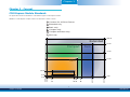 8
8
-
 9
9
-
 10
10
-
 11
11
-
 12
12
-
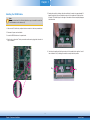 13
13
-
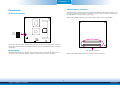 14
14
-
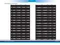 15
15
-
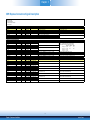 16
16
-
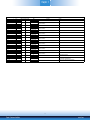 17
17
-
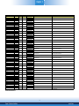 18
18
-
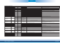 19
19
-
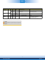 20
20
-
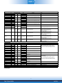 21
21
-
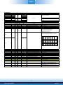 22
22
-
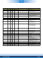 23
23
-
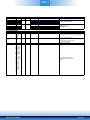 24
24
-
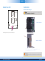 25
25
-
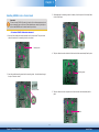 26
26
-
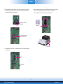 27
27
-
 28
28
-
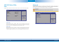 29
29
-
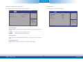 30
30
-
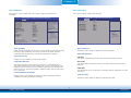 31
31
-
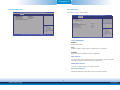 32
32
-
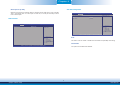 33
33
-
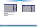 34
34
-
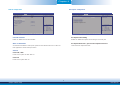 35
35
-
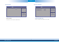 36
36
-
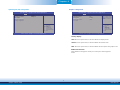 37
37
-
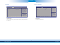 38
38
-
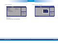 39
39
-
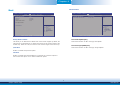 40
40
-
 41
41
-
 42
42
-
 43
43
-
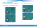 44
44
-
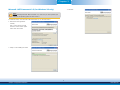 45
45
-
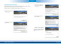 46
46
-
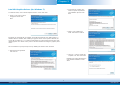 47
47
-
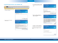 48
48
-
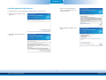 49
49
-
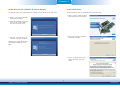 50
50
-
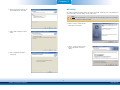 51
51
-
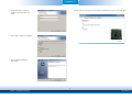 52
52
-
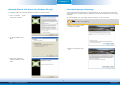 53
53
-
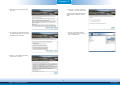 54
54
-
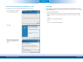 55
55
-
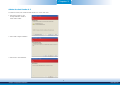 56
56
-
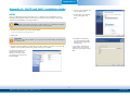 57
57
-
 58
58
-
 59
59
-
 60
60
-
 61
61
-
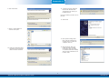 62
62
-
 63
63
-
 64
64
-
 65
65
-
 66
66


Ask a question and I''ll find the answer in the document
Finding information in a document is now easier with AI
Related papers
Other documents
-
ROHS EmETXe-i9652 User manual
-
 IBASE Technology ET981 User manual
-
Aaeon COM-WHUC6 User manual
-
-
ADLINK Technology com express User manual
-
-
-
 IBASE Technology ET975 User manual
-
 IBASE Technology ET970 User manual
-
VIA Technologies COME8X80 User manual


